EP1120900A2 - Apparatus for demodulating a frequency modulated signal , and method - Google Patents
Apparatus for demodulating a frequency modulated signal , and method Download PDFInfo
- Publication number
- EP1120900A2 EP1120900A2 EP00310077A EP00310077A EP1120900A2 EP 1120900 A2 EP1120900 A2 EP 1120900A2 EP 00310077 A EP00310077 A EP 00310077A EP 00310077 A EP00310077 A EP 00310077A EP 1120900 A2 EP1120900 A2 EP 1120900A2
- Authority
- EP
- European Patent Office
- Prior art keywords
- signal
- output
- demodulated
- product
- data slicer
- Prior art date
- Legal status (The legal status is an assumption and is not a legal conclusion. Google has not performed a legal analysis and makes no representation as to the accuracy of the status listed.)
- Withdrawn
Links
- 238000000034 method Methods 0.000 title claims description 23
- 230000003111 delayed effect Effects 0.000 claims description 6
- 238000001914 filtration Methods 0.000 claims 2
- 238000010586 diagram Methods 0.000 description 8
- 238000013461 design Methods 0.000 description 4
- 230000005540 biological transmission Effects 0.000 description 3
- 230000001413 cellular effect Effects 0.000 description 3
- 238000004519 manufacturing process Methods 0.000 description 3
- 238000011084 recovery Methods 0.000 description 2
- 239000013598 vector Substances 0.000 description 2
- 235000008694 Humulus lupulus Nutrition 0.000 description 1
- 230000032683 aging Effects 0.000 description 1
- 230000008901 benefit Effects 0.000 description 1
- 230000008859 change Effects 0.000 description 1
- 230000007613 environmental effect Effects 0.000 description 1
- 238000005259 measurement Methods 0.000 description 1
- 238000012986 modification Methods 0.000 description 1
- 230000004048 modification Effects 0.000 description 1
- 230000000737 periodic effect Effects 0.000 description 1
- 230000008569 process Effects 0.000 description 1
- 230000035484 reaction time Effects 0.000 description 1
- 230000009467 reduction Effects 0.000 description 1
- 230000001360 synchronised effect Effects 0.000 description 1
- 230000007704 transition Effects 0.000 description 1
Images


Classifications
-
- H—ELECTRICITY
- H03—ELECTRONIC CIRCUITRY
- H03D—DEMODULATION OR TRANSFERENCE OF MODULATION FROM ONE CARRIER TO ANOTHER
- H03D3/00—Demodulation of angle-, frequency- or phase- modulated oscillations
- H03D3/007—Demodulation of angle-, frequency- or phase- modulated oscillations by converting the oscillations into two quadrature related signals
Definitions
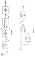
- the digitised signal is applied to the quadrature demodulator, comprised of multipliers 201 and 202, and oscillators 203 and 204.
- the signal generated by oscillator 203 is equal to cos(2 ⁇ f 1 ⁇ t), while the signal generated by oscillator 204 is equal to sin(2 ⁇ f 1 ⁇ t).
- Frequency f 1 is chosen such that the desired signal is mixed to baseband. Accordingly, in the illustrated embodiment f 1 is chosen to be 1.484 MHz.
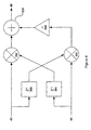
- the signals on lines 43 and 44 then pass to demodulator 30, shown in Figure 4.
- the complex envelope of the baseband signal is treated as a time series of sampled phasors, which are in fact vectors on the real and imaginary (or I and Q) axes. Accordingly, as the frequency deviation from the carrier of the transmitted signal increases, the frequency magnitude in the baseband signal increases, and in turn, the magnitude of the phase angle increases between two sampled phasors separated by a given time. Therefore, the phase angle between samples of the complex envelope is related to the original modulating signal.
- the direction of phasor rotation reflects the sign of the original modulating signal, or rather, the deviation of the modulated signal above or below the carrier.
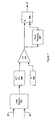
- matched filter 502 includes a 19-bit shift register 503, which is clocked by a 19X (921.6 kHz) clock signal on line 48.
- the shift register contents are then summed by adder 504.
- the running total of the shift register contents is compared to a constant value 9, block 505, by comparator 506.
- the output of comparator 506 therefore indicates whether the most prevalent bit value in the shift register is 1 or 0.
Landscapes
- Engineering & Computer Science (AREA)
- Power Engineering (AREA)
- Digital Transmission Methods That Use Modulated Carrier Waves (AREA)
Abstract
Description
CnxCn-1=1n·Qn-1 - Qn·In-1. The inputs to
Claims (22)
- A method for demodulating a frequency-modulated signal, which method comprises the following steps:whereby the output signal is representative of the demodulated signal.generating a first signal by fixing the modulated signal amplitude at a predetermined level;generating a second signal by delaying the first signal;generating an output signal by determining the cross product of the fixed-amplitude signal and the second signal;
- The method of claim 1, in which the second signal is delayed by a length of time such that the phase angle between the first and second signals is less than .2 pi, whereby the step of determining the cross product can be performed using a small-angle approximation.
- The method of claim 1 or 2, in which the step of fixing the signal amplitude is performed by applying the signal to a limiting amplifier.
- The method of claim 1, 2 or 3, in which the step of generating the first signal comprises the following substeps:whereby subsequent steps are performed in the digital signal domain.applying the signal to a limiting amplifier;digitising the output of the limiting amplifier;
- The method of claim 4, in which the substep of digitising the output of the limiting amplifier is performed by applying the output of the limiting amplifier to a flip-flop, whereby the flip-flop acts as a 1-bit analog-to-digital converter.
- The method of any preceding claim further comprising the step of squaring up the demodulated output signal by applying the output signal to a data slicer.
- The method of claim 6, in which the step of squaring up the demodulated output signal comprises the following substeps:whereby the comparator output consists of the squared up demodulated signal.generating a reference level signal by lowpass filtering the cross-product output;applying the output signal and the reference level signal to the inputs of a comparator;
- The method of claim 6, further comprising the step of applying the data slicer output to a matched filter to reduce the likelihood of errors in the demodulated signal.
- The method of claim 8, in which the number of taps in the matched filter is equal to the ratio between the data rate of the data slicer output and the bit rate of the demodulated signal.
- A method for demodulating a frequency modulated signal, which method comprises the following steps:amplifying the modulated signal using a limiting amplifier;digitising the limited signal using an analog-to-digital converter;applying the digitised limited signal to a quadrature demodulator to create a first I signal and a first Q signal;creating a second I signal by delaying the first I signal;creating a second Q signal by delaying the first Q signal;generating a first product by multiplying the first I signal by the second Q signal;generating a second product by multiplying the first Q signal by the second I signal;subtracting the second product from the first product to generate the demodulated signal.
- The method of claim 10, in which the step of digitising the limited signal is performed by applying the limited signal to a flip-flop, which acts as a 1-bit analog-to-digital converter.
- The method of claim 10 or 11, in which the second I signal and the second Q signal are each delayed by one sample.
- The method of claim 10, 11 or 12, further comprising the step of squaring up the demodulated signal by applying the demodulated signal to a data slicer.
- The method of claim 13, in which the step of squaring up the demodulated signal is comprised of the following substeps:generating a reference level signal by lowpass filtering the demodulated signal;comparing the demodulated signal with the reference level signal to generate a squared up output signal.
- The method of claim 13, further comprising the step of applying the data slicer output to a matched filter to reduce the likelihood of errors in the apparatus output.
- The method of claim 15, in which the number of taps in the matched filter is equal to the ratio between the data rate of the data slicer output and the bit rate of the demodulated signal.
- An apparatus for demodulating a frequency modulated signal, the apparatus comprising at least:a limiting amplifier, which amplifier's input receives the frequency modulated signal;an analog-to-digital converter, which converter operationally receives the limiting amplifier output signal and generates a digitised frequency modulated signal;a cross-product multiplier which receives the digitised frequency modulated signal and outputs the cross-product of the digitised frequency modulated signal with a delayed copy of the digitised frequency modulated signal to generate a demodulated output signal.
- The apparatus of claim 17, in which the analog-to-digital converter is a flip-flop generating a 1-bit digital output.
- The apparatus of claim 17 or 18, in which the cross-product multiplier is comprised of:whereby the adder output is the demodulated signal.a quadrature demodulator with an input connected to the analog-to-digital converter output, which quadrature demodulator generates a baseband I output and a baseband Q output;a first delay element, which element receives the I output of the quadrature demodulator;a second delay element, which element receives the Q output of the quadrature demodulator;a first multiplier, which multiplier has as its inputs the I output of the quadrature demodulator and the output of the second delay element;a second multiplier, which multiplier has as its inputs the Q output of the quadrature demodulator and the output of the first delay element;an inverter which receives the output of the second multiplier;an adder, which adder has as its inputs the output of the first multiplier and the output of the inverter;
- The apparatus of claim 17, 18 or 19, which apparatus is further comprised of a data slicer with input operably connected to the cross-product multiplier output.
- The apparatus of claim 20, in which the data slicer is comprised of:whereby the comparator outputs the squared up demodulated signal.a lowpass filter, which filter receives the data slicer input;a comparator with inputs of the data slicer input, and the lowpass filter output;
- The apparatus of claim 20, the apparatus further including a matched filter with input operably connected to the data slicer output, which matched filter provides for correction of errors in the data slicer output.
Applications Claiming Priority (2)
| Application Number | Priority Date | Filing Date | Title |
|---|---|---|---|
| CA292463 | 1999-12-17 | ||
| CA002292463A CA2292463C (en) | 1999-12-17 | 1999-12-17 | Digitally-implemented demodulator |
Publications (2)
| Publication Number | Publication Date |
|---|---|
| EP1120900A2 true EP1120900A2 (en) | 2001-08-01 |
| EP1120900A3 EP1120900A3 (en) | 2002-10-23 |
Family
ID=4164900
Family Applications (1)
| Application Number | Title | Priority Date | Filing Date |
|---|---|---|---|
| EP00310077A Withdrawn EP1120900A3 (en) | 1999-12-17 | 2000-11-13 | Apparatus for demodulating a frequency modulated signal , and method |
Country Status (3)
| Country | Link |
|---|---|
| US (1) | US6914946B1 (en) |
| EP (1) | EP1120900A3 (en) |
| CA (1) | CA2292463C (en) |
Families Citing this family (5)
| Publication number | Priority date | Publication date | Assignee | Title |
|---|---|---|---|---|
| TW550911B (en) * | 2001-06-21 | 2003-09-01 | Realtek Semiconductor Corp | FSK/GFSK signal receiver with the function of digitally compensating frequency offset and the receiving method of the same |
| GB0216703D0 (en) * | 2002-07-18 | 2002-08-28 | Koninkl Philips Electronics Nv | Receiver having a variable threshold slicer stage |
| US7903764B2 (en) * | 2004-05-10 | 2011-03-08 | Broadcom Corporation | Integrated burst FSK receiver |
| CN101160890A (en) * | 2005-04-08 | 2008-04-09 | 富士通株式会社 | Wireless devices that use the same carrier for transmission and reception |
| GB2518010A (en) * | 2013-09-09 | 2015-03-11 | Crfs Ltd | Frequency discriminator |
Family Cites Families (10)
| Publication number | Priority date | Publication date | Assignee | Title |
|---|---|---|---|---|
| EP0080014B1 (en) | 1981-09-26 | 1986-12-30 | Robert Bosch Gmbh | Digital demodulator for frequency-modulated signals |
| US4439756A (en) | 1982-01-20 | 1984-03-27 | International Telephone And Telegraph Corporation | Delta-Sigma modulator with switch capacitor implementation |
| JP2804755B2 (en) | 1986-09-01 | 1998-09-30 | 株式会社日立製作所 | FSK signal demodulation circuit |
| DE3808406A1 (en) | 1987-09-29 | 1989-04-06 | Wolfgang Lettner | DEVICE FOR GENERATING AERIAL IMAGES FROM MIRRORING |
| DE4309684C2 (en) | 1992-12-12 | 1995-11-23 | Ant Nachrichtentech | Process for demodulating frequency-modulated signals |
| AU683730B2 (en) * | 1994-04-04 | 1997-11-20 | Google Technology Holdings LLC | A wide bandwidth discriminator for use in a radio receiver |
| JP3508956B2 (en) * | 1995-04-13 | 2004-03-22 | ソニー株式会社 | Frequency modulation signal demodulation circuit and communication terminal device |
| JP3132802B2 (en) * | 1995-09-06 | 2001-02-05 | シャープ株式会社 | FM multiplex receiver |
| US6396953B1 (en) * | 1999-02-23 | 2002-05-28 | Rockwell Collins, Inc. | Data pattern correlator |
| JP3518430B2 (en) * | 1999-07-12 | 2004-04-12 | 三菱電機株式会社 | Digital FM demodulator |
-
1999
- 1999-12-17 CA CA002292463A patent/CA2292463C/en not_active Expired - Fee Related
-
2000
- 2000-10-25 US US09/696,410 patent/US6914946B1/en not_active Expired - Lifetime
- 2000-11-13 EP EP00310077A patent/EP1120900A3/en not_active Withdrawn
Also Published As
| Publication number | Publication date |
|---|---|
| CA2292463C (en) | 2005-04-12 |
| US6914946B1 (en) | 2005-07-05 |
| CA2292463A1 (en) | 2001-06-17 |
| EP1120900A3 (en) | 2002-10-23 |
Similar Documents
| Publication | Publication Date | Title |
|---|---|---|
| US6922555B1 (en) | Phase interpolation receiver for angle modulated RF signals | |
| EP0333266B1 (en) | A direct conversion receiver | |
| US7200188B2 (en) | Method and apparatus for frequency offset compensation | |
| JP4004553B2 (en) | Integrable radio receiver circuit for frequency modulated digital signals | |
| EP0883951B1 (en) | Receiver with filter offset correction | |
| US7787630B2 (en) | FM stereo decoder incorporating Costas loop pilot to stereo component phase correction | |
| KR100406224B1 (en) | Frequency modulation signaling inquiry and communication terminal equipment employing it | |
| US5640427A (en) | Demodulator | |
| US6549588B2 (en) | Communications system and corresponding receiver unit | |
| EP1643704B1 (en) | Frequency-shift-keying demodulator and method of frequency-shift-keying | |
| US7116964B2 (en) | Signal reception and processing method for cordless communications systems | |
| CA2292463C (en) | Digitally-implemented demodulator | |
| US6151371A (en) | Automatic frequency control circuit | |
| US6728321B2 (en) | Receiving device for angle-modulated signals | |
| EP1643635A2 (en) | Demodulator for use in wireless communications and receiver, method and terminal using it | |
| US20160226686A1 (en) | Receiving apparatus and receiving method | |
| US6002725A (en) | M-ary FSK receiver | |
| JP4449144B2 (en) | Carrier reproducing apparatus and method and receiving apparatus | |
| US20070189420A1 (en) | Limiter based analog demodulator | |
| RU2136115C1 (en) | Device for demodulation of multiple-position signals | |
| US20060111073A1 (en) | Demodulator of frequency modulated signals, and demodulating method of frequency modulated signals | |
| JPH0629746A (en) | Frequency tracking device | |
| JP3223402B2 (en) | Burst signal detection circuit | |
| JP2551261B2 (en) | Receiver circuit in spread spectrum wireless transmission | |
| US20080025438A1 (en) | Method and apparatus for demodulating saturated differential psk signals |
Legal Events
| Date | Code | Title | Description |
|---|---|---|---|
| PUAI | Public reference made under article 153(3) epc to a published international application that has entered the european phase |
Free format text: ORIGINAL CODE: 0009012 |
|
| AK | Designated contracting states |
Kind code of ref document: A2 Designated state(s): AT BE CH CY DE DK ES FI FR GB GR IE IT LI LU MC NL PT SE TR |
|
| AX | Request for extension of the european patent |
Free format text: AL;LT;LV;MK;RO;SI |
|
| PUAL | Search report despatched |
Free format text: ORIGINAL CODE: 0009013 |
|
| AK | Designated contracting states |
Kind code of ref document: A3 Designated state(s): AT BE CH CY DE DK ES FI FR GB GR IE IT LI LU MC NL PT SE TR |
|
| AX | Request for extension of the european patent |
Free format text: AL;LT;LV;MK;RO;SI |
|
| RIC1 | Information provided on ipc code assigned before grant |
Free format text: 7H 03D 3/02 A, 7H 03D 3/00 B |
|
| 17P | Request for examination filed |
Effective date: 20030422 |
|
| AKX | Designation fees paid |
Designated state(s): AT BE CH CY DE DK ES FI FR GB GR IE IT LI LU MC NL PT SE TR |
|
| 17Q | First examination report despatched |
Effective date: 20080212 |
|
| STAA | Information on the status of an ep patent application or granted ep patent |
Free format text: STATUS: THE APPLICATION IS DEEMED TO BE WITHDRAWN |
|
| 18D | Application deemed to be withdrawn |
Effective date: 20080823 |