EP1122561A1 - Alignement précis de composants optiques sur une couche de superstrat épaisse - Google Patents
Alignement précis de composants optiques sur une couche de superstrat épaisse Download PDFInfo
- Publication number
- EP1122561A1 EP1122561A1 EP00400287A EP00400287A EP1122561A1 EP 1122561 A1 EP1122561 A1 EP 1122561A1 EP 00400287 A EP00400287 A EP 00400287A EP 00400287 A EP00400287 A EP 00400287A EP 1122561 A1 EP1122561 A1 EP 1122561A1
- Authority
- EP
- European Patent Office
- Prior art keywords
- mask
- layer
- core layer
- substrate
- pattern
- Prior art date
- Legal status (The legal status is an assumption and is not a legal conclusion. Google has not performed a legal analysis and makes no representation as to the accuracy of the status listed.)
- Withdrawn
Links
- 230000003287 optical effect Effects 0.000 title claims abstract description 28
- 239000010410 layer Substances 0.000 claims abstract description 77
- 239000000758 substrate Substances 0.000 claims abstract description 43
- 239000012792 core layer Substances 0.000 claims abstract description 41
- 238000005530 etching Methods 0.000 claims abstract description 14
- 238000004519 manufacturing process Methods 0.000 claims abstract description 14
- 238000000034 method Methods 0.000 claims description 37
- 229910021417 amorphous silicon Inorganic materials 0.000 claims description 7
- 239000011819 refractory material Substances 0.000 claims description 7
- 239000002861 polymer material Substances 0.000 claims description 6
- 238000009832 plasma treatment Methods 0.000 claims description 4
- 239000000463 material Substances 0.000 abstract description 22
- VYPSYNLAJGMNEJ-UHFFFAOYSA-N Silicium dioxide Chemical compound O=[Si]=O VYPSYNLAJGMNEJ-UHFFFAOYSA-N 0.000 description 23
- 239000011162 core material Substances 0.000 description 22
- XUIMIQQOPSSXEZ-UHFFFAOYSA-N Silicon Chemical compound [Si] XUIMIQQOPSSXEZ-UHFFFAOYSA-N 0.000 description 13
- 239000010703 silicon Substances 0.000 description 13
- 229910052710 silicon Inorganic materials 0.000 description 12
- 239000000377 silicon dioxide Substances 0.000 description 11
- 238000010943 off-gassing Methods 0.000 description 6
- 230000003647 oxidation Effects 0.000 description 6
- 238000007254 oxidation reaction Methods 0.000 description 6
- 238000000151 deposition Methods 0.000 description 5
- 238000005137 deposition process Methods 0.000 description 5
- 238000005334 plasma enhanced chemical vapour deposition Methods 0.000 description 5
- 238000000623 plasma-assisted chemical vapour deposition Methods 0.000 description 5
- 238000001505 atmospheric-pressure chemical vapour deposition Methods 0.000 description 4
- 238000001459 lithography Methods 0.000 description 4
- 238000001020 plasma etching Methods 0.000 description 4
- 230000015572 biosynthetic process Effects 0.000 description 3
- 238000007796 conventional method Methods 0.000 description 3
- 230000008021 deposition Effects 0.000 description 3
- 239000007789 gas Substances 0.000 description 3
- GWEVSGVZZGPLCZ-UHFFFAOYSA-N Titan oxide Chemical compound O=[Ti]=O GWEVSGVZZGPLCZ-UHFFFAOYSA-N 0.000 description 2
- 230000004888 barrier function Effects 0.000 description 2
- YBMRDBCBODYGJE-UHFFFAOYSA-N germanium dioxide Chemical compound O=[Ge]=O YBMRDBCBODYGJE-UHFFFAOYSA-N 0.000 description 2
- 239000011521 glass Substances 0.000 description 2
- 238000000206 photolithography Methods 0.000 description 2
- 229920000642 polymer Polymers 0.000 description 2
- VYZAMTAEIAYCRO-UHFFFAOYSA-N Chromium Chemical compound [Cr] VYZAMTAEIAYCRO-UHFFFAOYSA-N 0.000 description 1
- 238000000137 annealing Methods 0.000 description 1
- QVGXLLKOCUKJST-UHFFFAOYSA-N atomic oxygen Chemical compound [O] QVGXLLKOCUKJST-UHFFFAOYSA-N 0.000 description 1
- 229910052804 chromium Inorganic materials 0.000 description 1
- 239000011651 chromium Substances 0.000 description 1
- 238000011109 contamination Methods 0.000 description 1
- 230000001351 cycling effect Effects 0.000 description 1
- 239000002019 doping agent Substances 0.000 description 1
- 238000005566 electron beam evaporation Methods 0.000 description 1
- 230000007062 hydrolysis Effects 0.000 description 1
- 238000006460 hydrolysis reaction Methods 0.000 description 1
- 229910052500 inorganic mineral Inorganic materials 0.000 description 1
- 239000013067 intermediate product Substances 0.000 description 1
- 229910052751 metal Inorganic materials 0.000 description 1
- 239000002184 metal Substances 0.000 description 1
- 150000001247 metal acetylides Chemical class 0.000 description 1
- 150000002739 metals Chemical class 0.000 description 1
- 239000011707 mineral Substances 0.000 description 1
- 229910021421 monocrystalline silicon Inorganic materials 0.000 description 1
- 230000005693 optoelectronics Effects 0.000 description 1
- 239000001301 oxygen Substances 0.000 description 1
- 229910052760 oxygen Inorganic materials 0.000 description 1
- 229920002120 photoresistant polymer Polymers 0.000 description 1
- 235000012239 silicon dioxide Nutrition 0.000 description 1
- 229910052814 silicon oxide Inorganic materials 0.000 description 1
- 238000004544 sputter deposition Methods 0.000 description 1
- 238000002207 thermal evaporation Methods 0.000 description 1
- 238000012876 topography Methods 0.000 description 1
- WFKWXMTUELFFGS-UHFFFAOYSA-N tungsten Chemical compound [W] WFKWXMTUELFFGS-UHFFFAOYSA-N 0.000 description 1
- 229910052721 tungsten Inorganic materials 0.000 description 1
- 239000010937 tungsten Substances 0.000 description 1
Images
Classifications
-
- G—PHYSICS
- G02—OPTICS
- G02B—OPTICAL ELEMENTS, SYSTEMS OR APPARATUS
- G02B6/00—Light guides; Structural details of arrangements comprising light guides and other optical elements, e.g. couplings
- G02B6/10—Light guides; Structural details of arrangements comprising light guides and other optical elements, e.g. couplings of the optical waveguide type
- G02B6/12—Light guides; Structural details of arrangements comprising light guides and other optical elements, e.g. couplings of the optical waveguide type of the integrated circuit kind
- G02B6/13—Integrated optical circuits characterised by the manufacturing method
- G02B6/136—Integrated optical circuits characterised by the manufacturing method by etching
-
- G—PHYSICS
- G02—OPTICS
- G02B—OPTICAL ELEMENTS, SYSTEMS OR APPARATUS
- G02B6/00—Light guides; Structural details of arrangements comprising light guides and other optical elements, e.g. couplings
- G02B6/10—Light guides; Structural details of arrangements comprising light guides and other optical elements, e.g. couplings of the optical waveguide type
- G02B6/12—Light guides; Structural details of arrangements comprising light guides and other optical elements, e.g. couplings of the optical waveguide type of the integrated circuit kind
- G02B6/13—Integrated optical circuits characterised by the manufacturing method
- G02B6/132—Integrated optical circuits characterised by the manufacturing method by deposition of thin films
-
- G—PHYSICS
- G02—OPTICS
- G02B—OPTICAL ELEMENTS, SYSTEMS OR APPARATUS
- G02B6/00—Light guides; Structural details of arrangements comprising light guides and other optical elements, e.g. couplings
- G02B6/10—Light guides; Structural details of arrangements comprising light guides and other optical elements, e.g. couplings of the optical waveguide type
- G02B6/12—Light guides; Structural details of arrangements comprising light guides and other optical elements, e.g. couplings of the optical waveguide type of the integrated circuit kind
- G02B2006/12166—Manufacturing methods
- G02B2006/12173—Masking
Definitions
- the present invention relates to the field of integrated optics, more particularly to the manufacture of planar lightwave circuits or lightwave optical circuits and the alignment of optical features and devices in superposed layers of such circuits.
- planar lightwave circuits PLC
- lightwave optical circuits LOC
- optical devices such as waveguides, gratings, detectors, etc.
- optical features such as mirrors, trenches, etc.
- first set of waveguides, filters, resonators, etc. created in a first layer formed on a substrate
- second set of waveguides, gratings, detectors, etc. formed in a second layer, superposed on the first layer.
- the problem arises of correctly aligning the features and devices of the upper layer with respect to those in the lower layer (or layers).
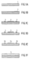
- Figure 1 illustrates the steps of a typical process for forming waveguides on a substrate.
- Figure 1A shows a typical substrate 1 made of silica and having a diameter of 100-150 mm.
- a first core glass layer 2 of around 6 ⁇ m thickness and made of doped silica, is deposited on the substrate 1, as illustrated in Fig.1B.
- the silica is doped with GeO 2 (sometimes with P 2 O 5 or B 2 O 3 added), but other dopants can be used, for example TiO 2 .
- the doped silica is deposited by any convenient technique, for example, flame hydrolysis deposition (FHD), plasma enhanced chemical vapour deposition (PECVD), atmospheric pressure chemical vapour deposition (APCVD), etc.
- a mask layer 3 is formed on the core layer 2, as illustrated in Fig. 1C, by a process such as PECVD, thermal or electron-beam evaporation, sputtering, etc.
- the mask 3 layer may be made of any suitable mineral material and typically has a thickness of 0.5 to 5 ⁇ m.
- the core layer 3 is patterned, using standard photolithography and etching processes (for example, reactive ion etching, RIE), so as to define the shapes of the cores of the waveguides which it is desired to form on the substrate, as well as alignment marks for use in subsequent processing.
- the core layer 2 is etched through the openings of the mask material by any suitable etching process (for example, RIE) to remove unwanted portions of the core layer, as illustrated in Fig.1D.
- the mask material is eliminated, for example by high pressure plasma etching, to leave only the desired core pattern 2a, and alignment marks 2b, as illustrated in Figure 1E.
- an overclad layer 4 typically 20 ⁇ m thick and made of silica (SiO 2 ) doped with B 2 O 3 and/or P 2 O 5 , is deposited over the etched core patterns by a process such as FHD, APCVD, etc., as illustrated in Fig.1F.
- the surface of the overclad layer 4 is not usually as flat as represented in Fig. 1F, it smoothly covers the cores of the waveguides.
- the overclad layer 4 When it is desired to create a new pattern in a layer superposed on the overclad layer 4, aligned with the underlying patterns, there is a problem because of low contrast of the core patterns and alignment marks under the overclad. Despite the transparency of the overclad material, the underlying core patterns and alignment marks have a fuzzy aspect because of the relatively large thickness of the overclad layer 4. Moreover, the smooth topography leads to a great uncertainty as to the location of the center of the core pattern with respect to which the superposed pattern is to be aligned.
- the conventional process could equally well have been described with reference to formation of waveguides on a silicon substrate.
- the preferred embodiments of the present invention provide a method for forming a planar lightwave circuit or lightwave optical circuit in which one or more high-visibility alignment marks are created in a core layer. These high-visibility alignment marks enable optical features and/or devices in superposed layers to be accurately aligned with respect to the lower core pattern(s).
- the present invention provides a method of manufacturing a planar lightwave circuit or lightwave optical circuit, comprising the following steps: providing a substrate layer; forming a core layer on said substrate layer; creating a mask on said core layer, said mask being formed of a refractory material, and said mask comprising a first portion defining a first pattern and a second portion defining a second pattern, said first pattern corresponding to a desired pattern to be formed in the core layer and said second pattern corresponding to one or more alignment marks; etching said core layer through said mask whereby to expose portions of said substrate not overlaid by said first and second portions of the mask; removing said first portion of said mask whereby to expose said desired pattern in the core layer while leaving said second portion of the mask in place; forming an overclad layer on said exposed portions of said substrate, said desired pattern in the core layer and said second portion of the mask.
- the present invention also provides a method of aligning optical devices in a planar lightwave circuit or lightwave optical circuit, comprising the following steps: creating a first circuit layer by providing a substrate layer, forming a core layer on said substrate layer, creating a mask on said core layer, said mask being formed of a refractory material, and said mask comprising a first portion defining a first pattern and a second portion defining a second pattern, said first pattern corresponding to a desired pattern to be formed in the core layer and said second pattern corresponding to one or more alignment marks, etching said core layer through said mask whereby to expose portions of said substrate not overlaid by said first and second portions of the mask, removing said first portion of said mask whereby to expose said desired pattern in the core layer while leaving said second portion of the mask in place, and forming an overclad layer on said exposed portions of said substrate, said desired pattern in the core layer and said second portion of the mask; and creating a second circuit layer, overlaid on said first circuit layer, said second circuit layer comprising at least one
- the methods according to the invention provide the advantage that they create alignment marks which, because of the mask material remaining thereon, are highly visible, even through a relatively thick overclad layer (of the order of 10's of micrometers). Moreover, because the alignment marks are formed on the substrate in the same lithography/etching steps as the core patterns on the substrate, the relative positions of the alignment marks and these core patterns are very accurately defined (auto-alignment). Indeed, the accuracy of the alignment is defined by the accuracy of the master mask and can be better than 0.1 ⁇ m. Furthermore, the highly-visible alignment marks are created by a very simple process using standard processing.
- the mask is made of a refractory material in view of the need to withstand the high temperatures (typically 800°C to 1300°C) involved in creation of the overclad layer.
- the mask material is silicon.
- Use of a silicon mask results in alignment marks having a highly-visible, metallic aspect.
- the silicon mask material is fully compatible with silicon and silicon dioxide layers (such as those used in the substrate and core layers) there will be no contamination of the optical layers by the mask material during the process of forming the overclad layer.
- the partial oxidation step can involve subjecting the second mask portion to a temperature of around 1000°C for approximately at least 5 minutes in ambient atmosphere.
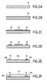
- a mask layer 30 is formed on the core layer 20, as illustrated in Fig.2C.
- the mask is made of amorphous silicon 0.5-5 ⁇ m thick, deposited and patterned by any conventional technique.
- the mask is patterned so as to have two portions: a first portion 30 defines the shapes of the cores of the waveguides (or other optical devices) which it is desired to form on the substrate 20, whereas a second portion 35 defines one or more alignment marks. It is the shape of the opening(s) in the first portion (30) of the mask which corresponds to the shape of the desired core pattern(s), whereas it is the shape of the second mask portion (35) itself which corresponds to the shape of the alignment mark(s).
- a plurality of alignment marks are formed (for example, two), each having a cross-shape with a width of a few micrometers.
- the core layer 20 is etched through the openings of the mask material, by any convenient process, to leave both the desired pattern 20a in the core material and alignment marks 20b, as illustrated in Fig.2D.
- the first portion 30 of the mask material is now eliminated to leave the desired core pattern 20' exposed, without removing the second mask portion 35, as illustrated in Figure 2E.
- the first mask portion 30 can be removed from the etched core layer (while leaving the second mask portion in place) by using a specific lithography step to define an auxiliary mask shielding the second mask portion, then etching (for example, using standard photolithography and high pressure etching techniques) to remove the first mask portion, and removing this auxiliary mask by conventional methods.
- the alignment marks are sufficiently far away from the core pattern(s)
- a drop of polymer for example standard photoresist
- an overclad layer 40 made of doped silica as in the conventional process and typically 20 ⁇ m thick, is deposited over the etched core pattern(s) 20' and masked alignment marks (35), as illustrated in Fig.2F.
- Deposition of the overclad layer involves a process such as PECVD, APCVD, FHD etc. performed at a temperature of 300°C to 1300°C followed by an annealing process cycling between 800°C and 1300°C.
- the mask material 35 is not destroyed by this overclad-deposition process because it is a refractory material, moreover the optical layers are not contaminated because the mask material has been chosen to be silicon, which is compatible with the optical layers.
- the additional step consists of partially oxidising the second portion 35 of the mask, before forming the overclad layer.
- This partial oxidation step oxidises the exterior portion of each grain of the amorphous silicon mask material, leaving the center portion of the grain unaffected (i.e. still silicon). This creates a barrier layer overlying the alignment marks, which prevents the outgassing phenomenon. Complete oxidation of the mask material 35 is to be avoided as this would render the mask material transparent and fail to enhance visibility of the alignment marks 20b.
- the partial oxidation step may be performed by subjecting the second mask portion 35 to a temperature of around 1000°C for 5 to 10 minutes in ambient atmosphere. This results in a layer of partially-oxidised silicon, overlying the alignment marks, which has a reddish color and is highly-visible even after deposition of the overclad layer. Incidentally, the alignment marks are highly-visible both on transparent substrates and on opaque substrates.
- the mask material used was amorphous silicon.
- the present invention is not limited to the use of such a material. More generally, other non-transparent, refractory materials may be used, for example SiC or other carbides, metals (for example tungsten and chromium), etc.
- metals for example tungsten and chromium
Landscapes
- Physics & Mathematics (AREA)
- Engineering & Computer Science (AREA)
- Microelectronics & Electronic Packaging (AREA)
- General Physics & Mathematics (AREA)
- Optics & Photonics (AREA)
- Optical Integrated Circuits (AREA)
Priority Applications (4)
| Application Number | Priority Date | Filing Date | Title |
|---|---|---|---|
| EP00400287A EP1122561A1 (fr) | 2000-02-03 | 2000-02-03 | Alignement précis de composants optiques sur une couche de superstrat épaisse |
| US09/735,774 US6547976B2 (en) | 2000-02-03 | 2000-12-13 | High precision alignment of optical waveguide features |
| AU2001230760A AU2001230760A1 (en) | 2000-02-03 | 2000-12-20 | High precision alignment of optical waveguide features |
| PCT/US2000/034815 WO2001057566A2 (fr) | 2000-02-03 | 2000-12-20 | Alignement haute precision d'elements de guides d'ondes optiques |
Applications Claiming Priority (1)
| Application Number | Priority Date | Filing Date | Title |
|---|---|---|---|
| EP00400287A EP1122561A1 (fr) | 2000-02-03 | 2000-02-03 | Alignement précis de composants optiques sur une couche de superstrat épaisse |
Publications (1)
| Publication Number | Publication Date |
|---|---|
| EP1122561A1 true EP1122561A1 (fr) | 2001-08-08 |
Family
ID=8173529
Family Applications (1)
| Application Number | Title | Priority Date | Filing Date |
|---|---|---|---|
| EP00400287A Withdrawn EP1122561A1 (fr) | 2000-02-03 | 2000-02-03 | Alignement précis de composants optiques sur une couche de superstrat épaisse |
Country Status (4)
| Country | Link |
|---|---|
| US (1) | US6547976B2 (fr) |
| EP (1) | EP1122561A1 (fr) |
| AU (1) | AU2001230760A1 (fr) |
| WO (1) | WO2001057566A2 (fr) |
Cited By (5)
| Publication number | Priority date | Publication date | Assignee | Title |
|---|---|---|---|---|
| EP1291692A1 (fr) * | 2001-09-07 | 2003-03-12 | Agilent Technologies Inc | Dispositif de guide d'ondes optiques plan |
| GB2403065A (en) * | 2003-05-20 | 2004-12-22 | Lg Philips Lcd Co Ltd | Crystallizing amorphous silicon using an align key |
| EP2000837A1 (fr) * | 2007-06-07 | 2008-12-10 | Nitto Denko Corporation | Procédé de fabrication de guide d'ondes optique |
| CN101369036B (zh) * | 2007-06-07 | 2011-12-21 | 日东电工株式会社 | 光波导路径的制造方法 |
| CN102565941A (zh) * | 2010-12-22 | 2012-07-11 | 日东电工株式会社 | 光波导路的制造方法 |
Families Citing this family (5)
| Publication number | Priority date | Publication date | Assignee | Title |
|---|---|---|---|---|
| US6731843B2 (en) * | 2000-12-29 | 2004-05-04 | Intel Corporation | Multi-level waveguide |
| KR100418908B1 (ko) * | 2001-12-21 | 2004-02-14 | 엘지전자 주식회사 | 광도파로용 실리카막 제조방법 |
| US6885803B2 (en) | 2003-07-14 | 2005-04-26 | Headway Technologies, Inc. | Method to produce stress-free optical waveguides to reduce stress-induced birefringence in planar lightwave circuit (PLC) devices |
| US7563628B2 (en) * | 2004-11-10 | 2009-07-21 | Lehigh University | Fabrication of optical waveguide devices |
| JP5055193B2 (ja) * | 2008-04-24 | 2012-10-24 | 日東電工株式会社 | 光電気混載基板の製造方法 |
Citations (6)
| Publication number | Priority date | Publication date | Assignee | Title |
|---|---|---|---|---|
| EP0318267A1 (fr) * | 1987-11-26 | 1989-05-31 | Corning Glass Works | Procédé de production d'un composant optique intégré |
| JPH06118256A (ja) * | 1992-10-09 | 1994-04-28 | Furukawa Electric Co Ltd:The | 石英系光導波路部品およびその製造方法 |
| JPH06160656A (ja) * | 1992-11-16 | 1994-06-07 | Ngk Insulators Ltd | 光集積回路の製造方法 |
| US5529595A (en) * | 1992-05-20 | 1996-06-25 | The Furukawa Electric Co., Ltd. | Method of positioning elements of an optical integrated circuit |
| EP0798768A1 (fr) * | 1996-03-25 | 1997-10-01 | Alcatel N.V. | Procédé pour fabriquer un composant optique à substrat de silicium cristallin |
| US5841931A (en) * | 1996-11-26 | 1998-11-24 | Massachusetts Institute Of Technology | Methods of forming polycrystalline semiconductor waveguides for optoelectronic integrated circuits, and devices formed thereby |
Family Cites Families (2)
| Publication number | Priority date | Publication date | Assignee | Title |
|---|---|---|---|---|
| FR2727768B1 (fr) | 1994-12-05 | 1997-01-10 | Alcatel Nv | Procede pour former une couche de silice a eliminer ulterieurement et procede pour rapporter un composant en optique integree |
| FR2766582A1 (fr) | 1997-07-23 | 1999-01-29 | Corning Inc | Methode de fabrication de composant optique et composant optique fabrique selon cette methode |
-
2000
- 2000-02-03 EP EP00400287A patent/EP1122561A1/fr not_active Withdrawn
- 2000-12-13 US US09/735,774 patent/US6547976B2/en not_active Expired - Fee Related
- 2000-12-20 WO PCT/US2000/034815 patent/WO2001057566A2/fr not_active Ceased
- 2000-12-20 AU AU2001230760A patent/AU2001230760A1/en not_active Abandoned
Patent Citations (6)
| Publication number | Priority date | Publication date | Assignee | Title |
|---|---|---|---|---|
| EP0318267A1 (fr) * | 1987-11-26 | 1989-05-31 | Corning Glass Works | Procédé de production d'un composant optique intégré |
| US5529595A (en) * | 1992-05-20 | 1996-06-25 | The Furukawa Electric Co., Ltd. | Method of positioning elements of an optical integrated circuit |
| JPH06118256A (ja) * | 1992-10-09 | 1994-04-28 | Furukawa Electric Co Ltd:The | 石英系光導波路部品およびその製造方法 |
| JPH06160656A (ja) * | 1992-11-16 | 1994-06-07 | Ngk Insulators Ltd | 光集積回路の製造方法 |
| EP0798768A1 (fr) * | 1996-03-25 | 1997-10-01 | Alcatel N.V. | Procédé pour fabriquer un composant optique à substrat de silicium cristallin |
| US5841931A (en) * | 1996-11-26 | 1998-11-24 | Massachusetts Institute Of Technology | Methods of forming polycrystalline semiconductor waveguides for optoelectronic integrated circuits, and devices formed thereby |
Non-Patent Citations (1)
| Title |
|---|
| PATENT ABSTRACTS OF JAPAN vol. 018, no. 478 (P - 1796) 6 September 1994 (1994-09-06) * |
Cited By (12)
| Publication number | Priority date | Publication date | Assignee | Title |
|---|---|---|---|---|
| EP1291692A1 (fr) * | 2001-09-07 | 2003-03-12 | Agilent Technologies Inc | Dispositif de guide d'ondes optiques plan |
| US6744953B2 (en) | 2001-09-07 | 2004-06-01 | Agilent Technologies, Inc. | Planar optical waveguide with alignment structure |
| GB2403065A (en) * | 2003-05-20 | 2004-12-22 | Lg Philips Lcd Co Ltd | Crystallizing amorphous silicon using an align key |
| GB2403065B (en) * | 2003-05-20 | 2006-07-12 | Lg Philips Lcd Co Ltd | Method of fabricating polycrystalline silicon and switching device using polycrystalline silicon |
| US7180198B2 (en) | 2003-05-20 | 2007-02-20 | Lg.Philips Lcd Co., Ltd. | Method of fabricating polycrystalline silicon and switching device using polycrystalline silicon |
| DE102004024924B4 (de) * | 2003-05-20 | 2007-12-13 | Lg.Philips Lcd Co., Ltd. | Verfahren zum Herstellen polykristallinen Siliciums, Verfahren zum Herstellen einer Ausrichtungsmarkierung, sowie Verfahren zum Herstellen eines Schaltelements |
| US7326598B2 (en) | 2003-05-20 | 2008-02-05 | Lg.Philips Lcd Co., Ltd. | Method of fabricating polycrystalline silicon |
| EP2000837A1 (fr) * | 2007-06-07 | 2008-12-10 | Nitto Denko Corporation | Procédé de fabrication de guide d'ondes optique |
| US7989150B2 (en) | 2007-06-07 | 2011-08-02 | Nitto Denko Corporation | Manufacturing method of optical waveguide |
| CN101369036B (zh) * | 2007-06-07 | 2011-12-21 | 日东电工株式会社 | 光波导路径的制造方法 |
| CN102565941A (zh) * | 2010-12-22 | 2012-07-11 | 日东电工株式会社 | 光波导路的制造方法 |
| CN102565941B (zh) * | 2010-12-22 | 2016-01-20 | 日东电工株式会社 | 光波导路的制造方法 |
Also Published As
| Publication number | Publication date |
|---|---|
| WO2001057566A2 (fr) | 2001-08-09 |
| AU2001230760A1 (en) | 2001-08-14 |
| WO2001057566A3 (fr) | 2002-01-03 |
| US20020074308A1 (en) | 2002-06-20 |
| US6547976B2 (en) | 2003-04-15 |
Similar Documents
| Publication | Publication Date | Title |
|---|---|---|
| KR100229560B1 (ko) | 마스크 정렬 마크제조 방법 | |
| KR101197804B1 (ko) | 위상 시프트 마스크의 제조방법 | |
| US6083843A (en) | Method of manufacturing planar lightwave circuits | |
| US6547976B2 (en) | High precision alignment of optical waveguide features | |
| KR101560385B1 (ko) | 위상 쉬프트 마스크 블랭크, 위상 쉬프트 마스크 및 그 제조 방법 | |
| NL8701478A (nl) | Werkwijze voor het vervaardigen van een planaire optische component. | |
| JP3002961B2 (ja) | 位相反転マスク及びその製造方法 | |
| JPH0643311A (ja) | 回折光学素子及びその製造方法 | |
| US6756319B2 (en) | Silica microstructure and fabrication method thereof | |
| US6759173B2 (en) | Single mask process for patterning microchip having grayscale and micromachined features | |
| AU8291498A (en) | Method of fabricating an optical component and optical component made thereby | |
| EP0570940A1 (fr) | Méthode de fabrication d'une composante optique | |
| JP3257130B2 (ja) | エッジ強調型位相シフトマスクの製造方法 | |
| JPS6211491B2 (fr) | ||
| JP2745988B2 (ja) | フォトマスクの製造方法 | |
| US6511777B1 (en) | Method for manufacturing a phase shift photomask | |
| JPH03284707A (ja) | 石英系光導波路の製造方法 | |
| JP3809792B2 (ja) | 光導波路の製造方法 | |
| JPH0728225A (ja) | 位相シフトマスク及びその製造方法 | |
| JP3571843B2 (ja) | ハイブリッド光集積回路の製造方法 | |
| KR100310937B1 (ko) | 초전도소자의포토리소그라피방법 | |
| CN113539797A (zh) | 半导体器件及其制造方法 | |
| JPH10206665A (ja) | 石英系光導波路の製造方法 | |
| KR19990012248A (ko) | 광도파로 소자의 제작방법 | |
| JPS63271206A (ja) | 導波路形光回折素子の製造方法 |
Legal Events
| Date | Code | Title | Description |
|---|---|---|---|
| PUAI | Public reference made under article 153(3) epc to a published international application that has entered the european phase |
Free format text: ORIGINAL CODE: 0009012 |
|
| AK | Designated contracting states |
Kind code of ref document: A1 Designated state(s): DE FR GB IT |
|
| AX | Request for extension of the european patent |
Free format text: AL;LT;LV;MK;RO;SI |
|
| 17P | Request for examination filed |
Effective date: 20011113 |
|
| AKX | Designation fees paid |
Free format text: DE FR GB IT |
|
| STAA | Information on the status of an ep patent application or granted ep patent |
Free format text: STATUS: THE APPLICATION IS DEEMED TO BE WITHDRAWN |
|
| 18D | Application deemed to be withdrawn |
Effective date: 20030902 |