EP1122742A2 - Méthode de test du dispositif de rafraíchissement d'une mémoire de données - Google Patents
Méthode de test du dispositif de rafraíchissement d'une mémoire de données Download PDFInfo
- Publication number
- EP1122742A2 EP1122742A2 EP01101749A EP01101749A EP1122742A2 EP 1122742 A2 EP1122742 A2 EP 1122742A2 EP 01101749 A EP01101749 A EP 01101749A EP 01101749 A EP01101749 A EP 01101749A EP 1122742 A2 EP1122742 A2 EP 1122742A2
- Authority
- EP
- European Patent Office
- Prior art keywords
- cell
- refresh
- state
- cells
- test
- Prior art date
- Legal status (The legal status is an assumption and is not a legal conclusion. Google has not performed a legal analysis and makes no representation as to the accuracy of the status listed.)
- Withdrawn
Links
- 238000012360 testing method Methods 0.000 title claims abstract description 90
- 230000015654 memory Effects 0.000 title claims abstract description 37
- 238000000034 method Methods 0.000 title claims abstract description 20
- 230000014759 maintenance of location Effects 0.000 claims abstract description 23
- 238000012795 verification Methods 0.000 claims abstract description 8
- 210000004027 cell Anatomy 0.000 claims description 137
- 238000004519 manufacturing process Methods 0.000 claims description 3
- 210000004460 N cell Anatomy 0.000 claims description 2
- 238000010998 test method Methods 0.000 description 7
- 230000007257 malfunction Effects 0.000 description 5
- 230000006870 function Effects 0.000 description 3
- 230000006399 behavior Effects 0.000 description 2
- 239000003990 capacitor Substances 0.000 description 2
- 238000013461 design Methods 0.000 description 2
- 238000001514 detection method Methods 0.000 description 2
- 238000011156 evaluation Methods 0.000 description 2
- 239000011159 matrix material Substances 0.000 description 2
- 230000004048 modification Effects 0.000 description 2
- 238000012986 modification Methods 0.000 description 2
- 230000008569 process Effects 0.000 description 2
- 239000004065 semiconductor Substances 0.000 description 2
- 208000003028 Stuttering Diseases 0.000 description 1
- 230000003213 activating effect Effects 0.000 description 1
- 230000004913 activation Effects 0.000 description 1
- 230000008901 benefit Effects 0.000 description 1
- 230000000903 blocking effect Effects 0.000 description 1
- 230000008859 change Effects 0.000 description 1
- 125000004122 cyclic group Chemical group 0.000 description 1
- 238000007689 inspection Methods 0.000 description 1
- 230000003993 interaction Effects 0.000 description 1
- 238000012545 processing Methods 0.000 description 1
- 238000011084 recovery Methods 0.000 description 1
- 230000000717 retained effect Effects 0.000 description 1
- 239000007787 solid Substances 0.000 description 1
- 210000002023 somite Anatomy 0.000 description 1
- 239000000126 substance Substances 0.000 description 1
- 230000002123 temporal effect Effects 0.000 description 1
Images
Classifications
-
- G—PHYSICS
- G11—INFORMATION STORAGE
- G11C—STATIC STORES
- G11C29/00—Checking stores for correct operation ; Subsequent repair; Testing stores during standby or offline operation
- G11C29/02—Detection or location of defective auxiliary circuits, e.g. defective refresh counters
Definitions
- the present invention relates generally to information stores, who need a refreshing device in order to information held in the memory cells at certain time intervals freshen up.
- the invention relates in detail a method for testing such a refresh device, according to the preamble of claim 1.
- DRAMs Dynamic Random Access Memories
- DRAMs Dynamic Random Access Memories
- capacitive memory cells mentioned above can also use different types of memory cells for a refresh need. Generally this applies to all types of memory cells, in which at least one of the information descriptors Conditions is volatile. These states can be arbitrary be physical or chemical in nature.
- a refresher basically includes the following: the cell state is sensed in good time before it changes could have evaporated so far that the one he represented Information would no longer be clearly recognizable; then the cell state is recognized from the sensed cell state Information freshly registered in the cell in question.
- the shelf life of information in a cell i.e. the "retention time” about which the registered information remains clearly recognizable in the cell is due to the design and can be within the same memory module from Cell to cell be very different.
- capacitive storage DRAMs is the guaranteed minimum retention time a "1" (i.e. the one described by the H level Information) usually at a few milliseconds, while the actual retention time is "1" in some Cells happen to be far more in some cases even up to a few seconds.
- the temporal Clearances for the refreshment have to be made, however organizational reasons, after the guaranteed minimum retention time judge, i.e. the intervals between refreshments must not be longer than this period.
- the refresh device constructed in this way is normally operated automatically in such a way that the selection device all memory cells corresponding to one user-selected follow-up program selects that the Sensing device feels the state of each selected cell and that the restoring device fresh the cell in question puts in the state which of those from the felt State derived information corresponds.
- the said follow-up program the refresh selector must be so by the user be designed so that no cell longer than the guaranteed Minimum retention time of the memory remains unrefreshed.
- a malfunction can e.g. consist in the fact that Refresh dialing device in the set program is not correct follows. This can happen in particular if in said dialing device a cyclically operated refresh counter for the cyclically repeated selection of the addresses of the ones to be refreshed Cells or groups of cells is used and the Overflow function of this counter is not working properly or the counter stutters in another way.
- Another malfunction may be that a cell selected for sensing is not reached by the restoring device.
- the object of the invention is to test the refresh device an information store a method to provide, which provides statements in a short test period, based on which can be determined whether all components of the refresh device work properly. This object is achieved according to the invention by the characterizing features of the claim 1 solved. Advantageous embodiments of the invention are marked in the subclaims.
- the invention is basically based on two findings.
- the One finding is that the above mentioned problems with refresh tests ultimately stem from the fact that the intended Operation of the recovery device includes the order, restore information to the selected cell, which is the same as the previously sensed information is.
- a targeted departure of this intended operation namely a test mode with the order to restore one clearly other than the perceived information, practically all possible errors in all components of the refreshing device can reveal. That is, every mistake made by the Success of a real refresh operation would impair or could, is also evident in the result of the said Test operating mode of the restoring device.
- the test operating mode according to the invention is therefore the above bypassed the problems mentioned, and still maintains the test result unrestricted significance.
- the verification of cell conditions at the beginning of the test can consist of the states of those affected Feel cells, if they are still unknown, e.g. by normal reading of the information stored in it.
- the Verification can also be done by any known information through a normal write operation in the cells are inscribed (making reading unnecessary is).
- This known information does not have to affect everyone Cells are the same, but it is preferably so that all these cells are in the same known state.
- You need in the restoring device at a suitable location (where otherwise the level is present, which is the information of the previous one Cell state) describes only any defined solid Feed in level to one of the registered State distinguishable cell state leads.
- This new one (“Fresh”) cell condition doesn't even clearly need one To describe storage information, it can also be any Intermediate state.
- the new cell state to be set assigned one of the possible storage information, in the case binary memory cells about a "1" if the one previously written Information is a "0".
- refresh dialers include often a refresh counter that is generated by refresh clock pulses cyclically incrementable over a counting range which comprises N counts (0 to N-1) by one Amount of N cells or cell groups of memory in cyclic Address repetition for refreshing.
- the test method according to the invention is preferred performed so that after registered a known Information in the cells to be involved in the test and before the minimum retention time expires, the refresh counter is advanced by successive clock pulses, operating the restoring device in the test mode, to move the sequentially addressed cells into the to set "new" states specified by this operating mode. Then it is checked to what extent these new conditions have actually been achieved.
- the count value or to preset a defined one Count value (e.g. for a targeted reset to 0) the following test sequence is preferably implemented: First, all N elements to be selected (cells or cell groups) of the amount involved in the test normal registered letter set in a known state (for example at L level). Then, within the minimum retention time and operating the restoring device in the test mode, N successive clock pulses applied to the refresh counter, and the "new" states of the N elements are read out.
- N elements to be selected are set to a known state, and again within the minimum retention time, this time again with the operation of the restoring device in the test mode, N successive clock pulses applied to the refresh counter, and the resulting states of the N elements are read out.
- the interposition of the Y real refresh operations should guarantee that at least one of the two N-parts Test cycles includes an overflow of the refresh counter, see above that any overflow errors are reflected in the test result. That is, it is ensured that during the second Test cycle an overflow is encountered, provided this did not occur during the first test cycle.
- the number Y N / 2 becomes preferably chosen because it is the smallest of those numbers is the largest possible distance from integer multiples (including 0) of N. This also applies to any Optimal skipping and stalling in meter operation Probability that the overflow within one or another test cycle.
- the first reading shows the binary state "1" (H level) at addresses W 0 to W N-2 and the binary state “0” (L level) at address W N-1 ;
- the second reading shows the binary state “1” at the addresses W N-1 and W 0 and the binary state "0" (L level) at the addresses W 1 to W N-2 .
- the second test cycle can also have more than N-X + 1 clock pulses be created. However, a number of exactly N-X + 1 is sufficient generally to skip or stall in operation of the refresh counter safely over the measure of 1 clock pulse to recognize.
- a refreshment counter selects an entire row (M cells) in normal operation by selectively opening the relevant one Row address line ("word line”) while all column address lines (“bit lines”) are open. If there are N lines with the word line addresses W 0 to W N-1 , each of the N “elements” of the quantity to be selected by the refresh counter contains M cells. In order to test whether the addressing by the refresh counter works properly, it may be sufficient in the method according to the invention to observe only one of these cells in each row in the course of the test cycles, by verifying cell states before the test (for example when writing in) and when checking the cell status after the test (i.e. when reading) only one and the same column address is activated.
- the memory is often divided into several banks divided, i.e. in areas of word lines, so that a word line must be open at the same time in each bank may.
- For the refresh mode it follows that it is basically it is possible to refresh cells on b word lines at the same time, if b is the number of banks.
- This behavior can also with the refresh test method according to the invention are checked, by expanding the test patterns described above accordingly. Specifically, the cell states that in each case according to a test mode of the refresh device according to the invention be read out, malfunction of the refresh device with parallel refresh, with serial Refreshing and recognizing when refreshing according to mixed pattern, if you expand the test pattern accordingly.
- the test method according to the invention practically no additional hardware on the refresh device to be tested necessary.
- the only modification to be made is creating a switch between the normal refresh mode and the test mode of the Restoring device.
- the verification of cell states before the test operation by enrolling the same information as about the L level in all involved If there is a cell, the switch to test mode very simple: only one, from L level differentiated level (e.g. the H level) provided and at the appropriate time to the output of the restoring device to be laid.
- L level differentiated level e.g. the H level
- test mode it suffices to switch the transistor switch from to be controlled from the outside or its output electrode or the to apply such a potential to the bit line concerned, that when rewriting the test mode predefined cell state results. This can be done in a very easily done as shown below with reference to the attached Drawing is explained.
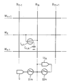
- the drawing figure shows schematically a section of a DRAM memory module with capacitive storage.
- a memory cell is shown in detail, which can be addressed via a word line WL n (row address line) and a bit line BL m (column address line).
- the cell consists of the storage capacitance C n, m , one side of which is connected to the reference potential (“ground”) and the other side of which is connected to the bit line BL m via the channel of an associated memory cell transistor (“selection transistor”) T n, m the word line WL n connected to the gate electrode of the transistor T n, m is driven.
- the memory module naturally contains a large number of further cells of the same type, which form a matrix of rows and columns, each row being assigned an individual word line and each column an individual bit line.
- each row being assigned an individual word line and each column an individual bit line.
- next to the word line WL n only the respectively immediately adjacent copies WL n-1, WL n + 1 next to the bit line BL and only the immediately adjacent copies BL m-1, BL m + 1 m shown.
- Each bit line (or each bit line pair in the case of paired or divided bit lines) is connected to an associated read / write circuit, which contains, among other things, a sense amplifier for sensing the state of charge of the storage capacity and a switch system for loading the storage capacity to selected voltage levels.
- the refresh test according to the invention can also be carried out in a simple manner without the addition of further hardware components. It is in fact easily possible to change the control of the bit lines so that instead of the output voltage of the sense amplifier LV m, the output voltage V 1 of the generator G is written directly into the cells. For this it is sufficient to carry out steps 1 to 4 in the sequence described above, with the only modification that the precharge switch S1 m is always closed (conductive) and the recharge switch S2 m is always open (thus never conductive). Each activation of the word line WL n then becomes a write access for the selected word line, the written information being dictated by the output voltage V 1 of the generator G.
- the modified sequence of steps is carried out for each selected word line.
Landscapes
- For Increasing The Reliability Of Semiconductor Memories (AREA)
- Techniques For Improving Reliability Of Storages (AREA)
- Dram (AREA)
Applications Claiming Priority (2)
| Application Number | Priority Date | Filing Date | Title |
|---|---|---|---|
| DE10004958 | 2000-02-04 | ||
| DE10004958A DE10004958A1 (de) | 2000-02-04 | 2000-02-04 | Verfahren zum Testen der Refresheinrichtung eines Informationsspeichers |
Publications (2)
| Publication Number | Publication Date |
|---|---|
| EP1122742A2 true EP1122742A2 (fr) | 2001-08-08 |
| EP1122742A3 EP1122742A3 (fr) | 2005-08-17 |
Family
ID=7629837
Family Applications (1)
| Application Number | Title | Priority Date | Filing Date |
|---|---|---|---|
| EP01101749A Withdrawn EP1122742A3 (fr) | 2000-02-04 | 2001-01-25 | Méthode de test du dispositif de rafraíchissement d'une mémoire de données |
Country Status (4)
| Country | Link |
|---|---|
| US (1) | US6779136B2 (fr) |
| EP (1) | EP1122742A3 (fr) |
| DE (1) | DE10004958A1 (fr) |
| TW (1) | TW495759B (fr) |
Families Citing this family (8)
| Publication number | Priority date | Publication date | Assignee | Title |
|---|---|---|---|---|
| DE10228527B3 (de) | 2002-06-26 | 2004-03-04 | Infineon Technologies Ag | Verfahren zum Überprüfen der Refresh-Funktion eines Informationsspeichers |
| TWI271743B (en) * | 2003-04-17 | 2007-01-21 | Winbond Electronics Corp | Method to adjust the refresh interval of adaptively controlled DRAM |
| US6958944B1 (en) * | 2004-05-26 | 2005-10-25 | Taiwan Semiconductor Manufacturing Co., Ltd. | Enhanced refresh circuit and method for reduction of DRAM refresh cycles |
| KR100625391B1 (ko) * | 2004-07-14 | 2006-09-20 | 주식회사 하이닉스반도체 | 리프레쉬를 수행하는 반도체 메모리 장치 |
| KR100691489B1 (ko) * | 2005-03-31 | 2007-03-09 | 주식회사 하이닉스반도체 | 반도체 기억 소자의 테스트용 셀프 리프레쉬 주기 선택회로 및 방법 |
| US7158434B2 (en) * | 2005-04-29 | 2007-01-02 | Infineon Technologies, Ag | Self-refresh circuit with optimized power consumption |
| US8176241B2 (en) * | 2006-04-05 | 2012-05-08 | Texas Instruments Incorporated | System and method for optimizing DRAM refreshes in a multi-channel memory controller |
| US9324433B2 (en) | 2011-04-25 | 2016-04-26 | Microsoft Technology Licensing, Llc | Intelligent flash reprogramming |
Family Cites Families (16)
| Publication number | Priority date | Publication date | Assignee | Title |
|---|---|---|---|---|
| DE3068578D1 (en) * | 1979-05-15 | 1984-08-23 | Mostek Corp | Method of testing the operation of an internal refresh counter in a random access memory and circuit for the testing thereof |
| US4347589A (en) * | 1979-05-15 | 1982-08-31 | Mostek Corporation | Refresh counter test |
| US4672583A (en) * | 1983-06-15 | 1987-06-09 | Nec Corporation | Dynamic random access memory device provided with test circuit for internal refresh circuit |
| US5321661A (en) * | 1991-11-20 | 1994-06-14 | Oki Electric Industry Co., Ltd. | Self-refreshing memory with on-chip timer test circuit |
| US5335202A (en) * | 1993-06-29 | 1994-08-02 | Micron Semiconductor, Inc. | Verifying dynamic memory refresh |
| US5446695A (en) * | 1994-03-22 | 1995-08-29 | International Business Machines Corporation | Memory device with programmable self-refreshing and testing methods therefore |
| JP3260583B2 (ja) * | 1995-04-04 | 2002-02-25 | 株式会社東芝 | ダイナミック型半導体メモリおよびそのテスト方法 |
| JPH10199296A (ja) * | 1997-01-09 | 1998-07-31 | Mitsubishi Electric Corp | ダイナミック型半導体記憶装置およびそのテスト方法 |
| US5903505A (en) * | 1997-05-19 | 1999-05-11 | Lsi Logic Corporation | Method of testing memory refresh operations wherein subthreshold leakage current may be set to near worst-case conditions |
| KR100258978B1 (ko) * | 1997-07-02 | 2000-06-15 | 윤종용 | 동적 메모리 테스트 회로의 어드레스 발생 장치 및방법 |
| US6330696B1 (en) * | 1998-08-13 | 2001-12-11 | Agere Systems Guardian Corp | Self-testing of DRAMs for multiple faults |
| US6317852B1 (en) * | 1998-10-23 | 2001-11-13 | Vanguard International Semiconductor Corporation | Method to test auto-refresh and self refresh circuitry |
| KR100309464B1 (ko) * | 1999-03-27 | 2001-09-26 | 김영환 | 리프레시 테스트 회로를 구비한 반도체 메모리 장치 |
| JP2002184181A (ja) * | 2000-03-24 | 2002-06-28 | Mitsubishi Electric Corp | 半導体記憶装置 |
| US6396744B1 (en) * | 2000-04-25 | 2002-05-28 | Multi Level Memory Technology | Flash memory with dynamic refresh |
| JP2001358313A (ja) * | 2000-06-14 | 2001-12-26 | Hitachi Ltd | 半導体装置 |
-
2000
- 2000-02-04 DE DE10004958A patent/DE10004958A1/de not_active Withdrawn
-
2001
- 2001-01-25 EP EP01101749A patent/EP1122742A3/fr not_active Withdrawn
- 2001-02-02 TW TW090102178A patent/TW495759B/zh not_active IP Right Cessation
- 2001-02-05 US US09/776,947 patent/US6779136B2/en not_active Expired - Fee Related
Also Published As
| Publication number | Publication date |
|---|---|
| EP1122742A3 (fr) | 2005-08-17 |
| DE10004958A1 (de) | 2001-08-09 |
| US6779136B2 (en) | 2004-08-17 |
| TW495759B (en) | 2002-07-21 |
| US20010027541A1 (en) | 2001-10-04 |
Similar Documents
| Publication | Publication Date | Title |
|---|---|---|
| DE10337855B4 (de) | Schaltung und Verfahren zur Auswertung und Steuerung einer Auffrischungsrate von Speicherzellen eines dynamischen Speichers | |
| DE3639169C2 (fr) | ||
| DE4017616C2 (fr) | ||
| DE102004053497A1 (de) | Halbleiterspeicherbauelement und Wiederauffrischverfahren | |
| DE2527486B2 (de) | Verfahren zur Prüfung bistabiler Speicherzellen | |
| EP0263470B1 (fr) | Procédé et agencements de test de modules de mémoire à mégabits à l'aide de configurations de test arbitraires dans le mode test multibits | |
| DE69516768T2 (de) | Prüfbarer i ddq- speicher durch kumulative wort-zeilen-aktivierung | |
| DE4034167A1 (de) | Halbleiterspeichereinrichtung und verfahren zum schnellen nachweis defekter speicherzellen | |
| EP0282976B1 (fr) | Procédé et aménagement de circuit pour l'écriture parallèle de données dans une mémoire à semi-conducteurs | |
| DE10022698A1 (de) | Halbleiterspeichereinrichtung | |
| DE10229802B3 (de) | Testschaltung und Verfahren zum Testen einer integrierten Speicherschaltung | |
| DE10134985A1 (de) | Test eines Halbleiterspeichers mit mehreren Speicherbänken | |
| EP1122742A2 (fr) | Méthode de test du dispositif de rafraíchissement d'une mémoire de données | |
| EP0286852B1 (fr) | Aménagement de circuit et procédé pour tester des cellules de mémoire | |
| DE10317364B4 (de) | Integrierter dynamischer Speicher mit Steuerungsschaltung zur Steuerung eines Refresh-Betriebs von Speicherzellen | |
| DE19501227B4 (de) | DRAM-Auffrisch-Steuerungsschaltung | |
| DE10329370B3 (de) | Schaltung und Verfahren zum Auffrischen von Speicherzellen eines dynamischen Speichers | |
| EP1163678B1 (fr) | Memoire integree avec cellules memoires presentant chacune un transistor memoire ferroelectrique | |
| DE10234944B4 (de) | Verfahren zum Testen eines Halbleiterspeichers mit mehreren Speicherbänken | |
| DE19913570C2 (de) | Betriebsverfahren für einen integrierten Speicher und integrierter Speicher | |
| DE4231169C2 (de) | Halbleiterspeichervorrichtung und Verfahren zum Betreiben einer solchen | |
| DE10110272B4 (de) | Halbleiterspeicher | |
| EP1678721A1 (fr) | Dispositif de memoire et procede permettant son fonctionnement | |
| DE10102350A1 (de) | Integrierter Speicher mit mehreren Speicherzellenfeldern sowie Verfahren zum Betrieb des integrierten Speichers | |
| DE10245696B3 (de) | Speicherschaltung und Verfahren zum Auslesen von Daten |
Legal Events
| Date | Code | Title | Description |
|---|---|---|---|
| PUAI | Public reference made under article 153(3) epc to a published international application that has entered the european phase |
Free format text: ORIGINAL CODE: 0009012 |
|
| AK | Designated contracting states |
Kind code of ref document: A2 Designated state(s): AT BE CH CY DE DK ES FI FR GB GR IE IT LI LU MC NL PT SE TR |
|
| AX | Request for extension of the european patent |
Free format text: AL;LT;LV;MK;RO;SI |
|
| PUAL | Search report despatched |
Free format text: ORIGINAL CODE: 0009013 |
|
| AK | Designated contracting states |
Kind code of ref document: A3 Designated state(s): AT BE CH CY DE DK ES FI FR GB GR IE IT LI LU MC NL PT SE TR |
|
| AX | Request for extension of the european patent |
Extension state: AL LT LV MK RO SI |
|
| 17P | Request for examination filed |
Effective date: 20050928 |
|
| AKX | Designation fees paid |
Designated state(s): DE GB IE IT |
|
| 17Q | First examination report despatched |
Effective date: 20060323 |
|
| STAA | Information on the status of an ep patent application or granted ep patent |
Free format text: STATUS: THE APPLICATION IS DEEMED TO BE WITHDRAWN |
|
| 18D | Application deemed to be withdrawn |
Effective date: 20090801 |