EP1122778A2 - Dispositif de circuit et son procédé de fabrication - Google Patents
Dispositif de circuit et son procédé de fabrication Download PDFInfo
- Publication number
- EP1122778A2 EP1122778A2 EP00308477A EP00308477A EP1122778A2 EP 1122778 A2 EP1122778 A2 EP 1122778A2 EP 00308477 A EP00308477 A EP 00308477A EP 00308477 A EP00308477 A EP 00308477A EP 1122778 A2 EP1122778 A2 EP 1122778A2
- Authority
- EP
- European Patent Office
- Prior art keywords
- conductive
- conductive paths
- circuit device
- circuit
- insulating resin
- Prior art date
- Legal status (The legal status is an assumption and is not a legal conclusion. Google has not performed a legal analysis and makes no representation as to the accuracy of the status listed.)
- Withdrawn
Links
Images





Classifications
-
- H—ELECTRICITY
- H05—ELECTRIC TECHNIQUES NOT OTHERWISE PROVIDED FOR
- H05K—PRINTED CIRCUITS; CASINGS OR CONSTRUCTIONAL DETAILS OF ELECTRIC APPARATUS; MANUFACTURE OF ASSEMBLAGES OF ELECTRICAL COMPONENTS
- H05K1/00—Printed circuits
- H05K1/18—Printed circuits structurally associated with non-printed electric components
- H05K1/182—Printed circuits structurally associated with non-printed electric components associated with components mounted in printed circuit boards [PCB], e.g. insert-mounted components [IMC]
- H05K1/185—Printed circuits structurally associated with non-printed electric components associated with components mounted in printed circuit boards [PCB], e.g. insert-mounted components [IMC] associated with components encapsulated in the insulating substrate of the PCBs; associated with components incorporated in internal layers of multilayer circuit boards
- H05K1/186—Printed circuits structurally associated with non-printed electric components associated with components mounted in printed circuit boards [PCB], e.g. insert-mounted components [IMC] associated with components encapsulated in the insulating substrate of the PCBs; associated with components incorporated in internal layers of multilayer circuit boards manufactured by mounting on or connecting to patterned circuits before or during embedding
- H05K1/187—Printed circuits structurally associated with non-printed electric components associated with components mounted in printed circuit boards [PCB], e.g. insert-mounted components [IMC] associated with components encapsulated in the insulating substrate of the PCBs; associated with components incorporated in internal layers of multilayer circuit boards manufactured by mounting on or connecting to patterned circuits before or during embedding the patterned circuits being prefabricated circuits, which are not yet attached to a permanent insulating substrate, e.g. on a temporary carrier
-
- H—ELECTRICITY
- H05—ELECTRIC TECHNIQUES NOT OTHERWISE PROVIDED FOR
- H05K—PRINTED CIRCUITS; CASINGS OR CONSTRUCTIONAL DETAILS OF ELECTRIC APPARATUS; MANUFACTURE OF ASSEMBLAGES OF ELECTRICAL COMPONENTS
- H05K1/00—Printed circuits
- H05K1/18—Printed circuits structurally associated with non-printed electric components
-
- H—ELECTRICITY
- H05—ELECTRIC TECHNIQUES NOT OTHERWISE PROVIDED FOR
- H05K—PRINTED CIRCUITS; CASINGS OR CONSTRUCTIONAL DETAILS OF ELECTRIC APPARATUS; MANUFACTURE OF ASSEMBLAGES OF ELECTRICAL COMPONENTS
- H05K1/00—Printed circuits
- H05K1/18—Printed circuits structurally associated with non-printed electric components
- H05K1/182—Printed circuits structurally associated with non-printed electric components associated with components mounted in printed circuit boards [PCB], e.g. insert-mounted components [IMC]
- H05K1/185—Printed circuits structurally associated with non-printed electric components associated with components mounted in printed circuit boards [PCB], e.g. insert-mounted components [IMC] associated with components encapsulated in the insulating substrate of the PCBs; associated with components incorporated in internal layers of multilayer circuit boards
- H05K1/188—Printed circuits structurally associated with non-printed electric components associated with components mounted in printed circuit boards [PCB], e.g. insert-mounted components [IMC] associated with components encapsulated in the insulating substrate of the PCBs; associated with components incorporated in internal layers of multilayer circuit boards manufactured by mounting on or attaching to a structure having a conductive layer, e.g. a metal foil, such that the terminals of the component are connected to or adjacent to the conductive layer before embedding, and by using the conductive layer, which is patterned after embedding, at least partially for connecting the component
-
- H—ELECTRICITY
- H10—SEMICONDUCTOR DEVICES; ELECTRIC SOLID-STATE DEVICES NOT OTHERWISE PROVIDED FOR
- H10W—GENERIC PACKAGES, INTERCONNECTIONS, CONNECTORS OR OTHER CONSTRUCTIONAL DETAILS OF DEVICES COVERED BY CLASS H10
- H10W70/00—Package substrates; Interposers; Redistribution layers [RDL]
- H10W70/01—Manufacture or treatment
- H10W70/04—Manufacture or treatment of leadframes
-
- H—ELECTRICITY
- H10—SEMICONDUCTOR DEVICES; ELECTRIC SOLID-STATE DEVICES NOT OTHERWISE PROVIDED FOR
- H10W—GENERIC PACKAGES, INTERCONNECTIONS, CONNECTORS OR OTHER CONSTRUCTIONAL DETAILS OF DEVICES COVERED BY CLASS H10
- H10W70/00—Package substrates; Interposers; Redistribution layers [RDL]
- H10W70/01—Manufacture or treatment
- H10W70/04—Manufacture or treatment of leadframes
- H10W70/042—Etching
-
- H—ELECTRICITY
- H10—SEMICONDUCTOR DEVICES; ELECTRIC SOLID-STATE DEVICES NOT OTHERWISE PROVIDED FOR
- H10W—GENERIC PACKAGES, INTERCONNECTIONS, CONNECTORS OR OTHER CONSTRUCTIONAL DETAILS OF DEVICES COVERED BY CLASS H10
- H10W74/00—Encapsulations, e.g. protective coatings
- H10W74/01—Manufacture or treatment
-
- H—ELECTRICITY
- H10—SEMICONDUCTOR DEVICES; ELECTRIC SOLID-STATE DEVICES NOT OTHERWISE PROVIDED FOR
- H10W—GENERIC PACKAGES, INTERCONNECTIONS, CONNECTORS OR OTHER CONSTRUCTIONAL DETAILS OF DEVICES COVERED BY CLASS H10
- H10W74/00—Encapsulations, e.g. protective coatings
- H10W74/10—Encapsulations, e.g. protective coatings characterised by their shape or disposition
- H10W74/111—Encapsulations, e.g. protective coatings characterised by their shape or disposition the semiconductor body being completely enclosed
-
- H—ELECTRICITY
- H10—SEMICONDUCTOR DEVICES; ELECTRIC SOLID-STATE DEVICES NOT OTHERWISE PROVIDED FOR
- H10W—GENERIC PACKAGES, INTERCONNECTIONS, CONNECTORS OR OTHER CONSTRUCTIONAL DETAILS OF DEVICES COVERED BY CLASS H10
- H10W90/00—Package configurations
-
- H—ELECTRICITY
- H05—ELECTRIC TECHNIQUES NOT OTHERWISE PROVIDED FOR
- H05K—PRINTED CIRCUITS; CASINGS OR CONSTRUCTIONAL DETAILS OF ELECTRIC APPARATUS; MANUFACTURE OF ASSEMBLAGES OF ELECTRICAL COMPONENTS
- H05K3/00—Apparatus or processes for manufacturing printed circuits
- H05K3/02—Apparatus or processes for manufacturing printed circuits in which the conductive material is applied to the surface of the insulating support and is thereafter removed from such areas of the surface which are not intended for current conducting or shielding
- H05K3/06—Apparatus or processes for manufacturing printed circuits in which the conductive material is applied to the surface of the insulating support and is thereafter removed from such areas of the surface which are not intended for current conducting or shielding the conductive material being removed chemically or electrolytically, e.g. by photo-etch process
-
- H—ELECTRICITY
- H05—ELECTRIC TECHNIQUES NOT OTHERWISE PROVIDED FOR
- H05K—PRINTED CIRCUITS; CASINGS OR CONSTRUCTIONAL DETAILS OF ELECTRIC APPARATUS; MANUFACTURE OF ASSEMBLAGES OF ELECTRICAL COMPONENTS
- H05K3/00—Apparatus or processes for manufacturing printed circuits
- H05K3/10—Apparatus or processes for manufacturing printed circuits in which conductive material is applied to the insulating support in such a manner as to form the desired conductive pattern
- H05K3/20—Apparatus or processes for manufacturing printed circuits in which conductive material is applied to the insulating support in such a manner as to form the desired conductive pattern by affixing prefabricated conductor pattern
- H05K3/202—Apparatus or processes for manufacturing printed circuits in which conductive material is applied to the insulating support in such a manner as to form the desired conductive pattern by affixing prefabricated conductor pattern using self-supporting metal foil pattern
-
- H—ELECTRICITY
- H10—SEMICONDUCTOR DEVICES; ELECTRIC SOLID-STATE DEVICES NOT OTHERWISE PROVIDED FOR
- H10P—GENERIC PROCESSES OR APPARATUS FOR THE MANUFACTURE OR TREATMENT OF DEVICES COVERED BY CLASS H10
- H10P72/00—Handling or holding of wafers, substrates or devices during manufacture or treatment thereof
- H10P72/70—Handling or holding of wafers, substrates or devices during manufacture or treatment thereof for supporting or gripping
- H10P72/74—Handling or holding of wafers, substrates or devices during manufacture or treatment thereof for supporting or gripping using temporarily an auxiliary support
- H10P72/7438—Handling or holding of wafers, substrates or devices during manufacture or treatment thereof for supporting or gripping using temporarily an auxiliary support with parts of the auxiliary support remaining in the finished device
-
- H—ELECTRICITY
- H10—SEMICONDUCTOR DEVICES; ELECTRIC SOLID-STATE DEVICES NOT OTHERWISE PROVIDED FOR
- H10W—GENERIC PACKAGES, INTERCONNECTIONS, CONNECTORS OR OTHER CONSTRUCTIONAL DETAILS OF DEVICES COVERED BY CLASS H10
- H10W70/00—Package substrates; Interposers; Redistribution layers [RDL]
- H10W70/40—Leadframes
-
- H—ELECTRICITY
- H10—SEMICONDUCTOR DEVICES; ELECTRIC SOLID-STATE DEVICES NOT OTHERWISE PROVIDED FOR
- H10W—GENERIC PACKAGES, INTERCONNECTIONS, CONNECTORS OR OTHER CONSTRUCTIONAL DETAILS OF DEVICES COVERED BY CLASS H10
- H10W72/00—Interconnections or connectors in packages
- H10W72/01—Manufacture or treatment
- H10W72/0198—Manufacture or treatment batch processes
-
- H—ELECTRICITY
- H10—SEMICONDUCTOR DEVICES; ELECTRIC SOLID-STATE DEVICES NOT OTHERWISE PROVIDED FOR
- H10W—GENERIC PACKAGES, INTERCONNECTIONS, CONNECTORS OR OTHER CONSTRUCTIONAL DETAILS OF DEVICES COVERED BY CLASS H10
- H10W72/00—Interconnections or connectors in packages
- H10W72/071—Connecting or disconnecting
- H10W72/072—Connecting or disconnecting of bump connectors
- H10W72/07251—Connecting or disconnecting of bump connectors characterised by changes in properties of the bump connectors during connecting
-
- H—ELECTRICITY
- H10—SEMICONDUCTOR DEVICES; ELECTRIC SOLID-STATE DEVICES NOT OTHERWISE PROVIDED FOR
- H10W—GENERIC PACKAGES, INTERCONNECTIONS, CONNECTORS OR OTHER CONSTRUCTIONAL DETAILS OF DEVICES COVERED BY CLASS H10
- H10W72/00—Interconnections or connectors in packages
- H10W72/071—Connecting or disconnecting
- H10W72/073—Connecting or disconnecting of die-attach connectors
- H10W72/07331—Connecting techniques
- H10W72/07336—Soldering or alloying
-
- H—ELECTRICITY
- H10—SEMICONDUCTOR DEVICES; ELECTRIC SOLID-STATE DEVICES NOT OTHERWISE PROVIDED FOR
- H10W—GENERIC PACKAGES, INTERCONNECTIONS, CONNECTORS OR OTHER CONSTRUCTIONAL DETAILS OF DEVICES COVERED BY CLASS H10
- H10W72/00—Interconnections or connectors in packages
- H10W72/071—Connecting or disconnecting
- H10W72/074—Connecting or disconnecting of anisotropic conductive adhesives
-
- H—ELECTRICITY
- H10—SEMICONDUCTOR DEVICES; ELECTRIC SOLID-STATE DEVICES NOT OTHERWISE PROVIDED FOR
- H10W—GENERIC PACKAGES, INTERCONNECTIONS, CONNECTORS OR OTHER CONSTRUCTIONAL DETAILS OF DEVICES COVERED BY CLASS H10
- H10W72/00—Interconnections or connectors in packages
- H10W72/071—Connecting or disconnecting
- H10W72/075—Connecting or disconnecting of bond wires
-
- H—ELECTRICITY
- H10—SEMICONDUCTOR DEVICES; ELECTRIC SOLID-STATE DEVICES NOT OTHERWISE PROVIDED FOR
- H10W—GENERIC PACKAGES, INTERCONNECTIONS, CONNECTORS OR OTHER CONSTRUCTIONAL DETAILS OF DEVICES COVERED BY CLASS H10
- H10W72/00—Interconnections or connectors in packages
- H10W72/071—Connecting or disconnecting
- H10W72/075—Connecting or disconnecting of bond wires
- H10W72/07531—Techniques
- H10W72/07532—Compression bonding, e.g. thermocompression bonding
- H10W72/07533—Ultrasonic bonding, e.g. thermosonic bonding
-
- H—ELECTRICITY
- H10—SEMICONDUCTOR DEVICES; ELECTRIC SOLID-STATE DEVICES NOT OTHERWISE PROVIDED FOR
- H10W—GENERIC PACKAGES, INTERCONNECTIONS, CONNECTORS OR OTHER CONSTRUCTIONAL DETAILS OF DEVICES COVERED BY CLASS H10
- H10W72/00—Interconnections or connectors in packages
- H10W72/20—Bump connectors, e.g. solder bumps or copper pillars; Dummy bumps; Thermal bumps
-
- H—ELECTRICITY
- H10—SEMICONDUCTOR DEVICES; ELECTRIC SOLID-STATE DEVICES NOT OTHERWISE PROVIDED FOR
- H10W—GENERIC PACKAGES, INTERCONNECTIONS, CONNECTORS OR OTHER CONSTRUCTIONAL DETAILS OF DEVICES COVERED BY CLASS H10
- H10W72/00—Interconnections or connectors in packages
- H10W72/30—Die-attach connectors
- H10W72/321—Structures or relative sizes of die-attach connectors
- H10W72/325—Die-attach connectors having a filler embedded in a matrix
-
- H—ELECTRICITY
- H10—SEMICONDUCTOR DEVICES; ELECTRIC SOLID-STATE DEVICES NOT OTHERWISE PROVIDED FOR
- H10W—GENERIC PACKAGES, INTERCONNECTIONS, CONNECTORS OR OTHER CONSTRUCTIONAL DETAILS OF DEVICES COVERED BY CLASS H10
- H10W72/00—Interconnections or connectors in packages
- H10W72/30—Die-attach connectors
- H10W72/351—Materials of die-attach connectors
- H10W72/352—Materials of die-attach connectors comprising metals or metalloids, e.g. solders
-
- H—ELECTRICITY
- H10—SEMICONDUCTOR DEVICES; ELECTRIC SOLID-STATE DEVICES NOT OTHERWISE PROVIDED FOR
- H10W—GENERIC PACKAGES, INTERCONNECTIONS, CONNECTORS OR OTHER CONSTRUCTIONAL DETAILS OF DEVICES COVERED BY CLASS H10
- H10W72/00—Interconnections or connectors in packages
- H10W72/30—Die-attach connectors
- H10W72/351—Materials of die-attach connectors
- H10W72/353—Materials of die-attach connectors not comprising solid metals or solid metalloids, e.g. ceramics
- H10W72/354—Materials of die-attach connectors not comprising solid metals or solid metalloids, e.g. ceramics comprising polymers
-
- H—ELECTRICITY
- H10—SEMICONDUCTOR DEVICES; ELECTRIC SOLID-STATE DEVICES NOT OTHERWISE PROVIDED FOR
- H10W—GENERIC PACKAGES, INTERCONNECTIONS, CONNECTORS OR OTHER CONSTRUCTIONAL DETAILS OF DEVICES COVERED BY CLASS H10
- H10W72/00—Interconnections or connectors in packages
- H10W72/50—Bond wires
- H10W72/531—Shapes of wire connectors
- H10W72/536—Shapes of wire connectors the connected ends being ball-shaped
-
- H—ELECTRICITY
- H10—SEMICONDUCTOR DEVICES; ELECTRIC SOLID-STATE DEVICES NOT OTHERWISE PROVIDED FOR
- H10W—GENERIC PACKAGES, INTERCONNECTIONS, CONNECTORS OR OTHER CONSTRUCTIONAL DETAILS OF DEVICES COVERED BY CLASS H10
- H10W72/00—Interconnections or connectors in packages
- H10W72/50—Bond wires
- H10W72/531—Shapes of wire connectors
- H10W72/5363—Shapes of wire connectors the connected ends being wedge-shaped
-
- H—ELECTRICITY
- H10—SEMICONDUCTOR DEVICES; ELECTRIC SOLID-STATE DEVICES NOT OTHERWISE PROVIDED FOR
- H10W—GENERIC PACKAGES, INTERCONNECTIONS, CONNECTORS OR OTHER CONSTRUCTIONAL DETAILS OF DEVICES COVERED BY CLASS H10
- H10W72/00—Interconnections or connectors in packages
- H10W72/50—Bond wires
- H10W72/541—Dispositions of bond wires
- H10W72/5449—Dispositions of bond wires not being orthogonal to a side surface of the chip, e.g. fan-out arrangements
-
- H—ELECTRICITY
- H10—SEMICONDUCTOR DEVICES; ELECTRIC SOLID-STATE DEVICES NOT OTHERWISE PROVIDED FOR
- H10W—GENERIC PACKAGES, INTERCONNECTIONS, CONNECTORS OR OTHER CONSTRUCTIONAL DETAILS OF DEVICES COVERED BY CLASS H10
- H10W72/00—Interconnections or connectors in packages
- H10W72/50—Bond wires
- H10W72/551—Materials of bond wires
- H10W72/552—Materials of bond wires comprising metals or metalloids, e.g. silver
-
- H—ELECTRICITY
- H10—SEMICONDUCTOR DEVICES; ELECTRIC SOLID-STATE DEVICES NOT OTHERWISE PROVIDED FOR
- H10W—GENERIC PACKAGES, INTERCONNECTIONS, CONNECTORS OR OTHER CONSTRUCTIONAL DETAILS OF DEVICES COVERED BY CLASS H10
- H10W72/00—Interconnections or connectors in packages
- H10W72/50—Bond wires
- H10W72/551—Materials of bond wires
- H10W72/552—Materials of bond wires comprising metals or metalloids, e.g. silver
- H10W72/5522—Materials of bond wires comprising metals or metalloids, e.g. silver comprising gold [Au]
-
- H—ELECTRICITY
- H10—SEMICONDUCTOR DEVICES; ELECTRIC SOLID-STATE DEVICES NOT OTHERWISE PROVIDED FOR
- H10W—GENERIC PACKAGES, INTERCONNECTIONS, CONNECTORS OR OTHER CONSTRUCTIONAL DETAILS OF DEVICES COVERED BY CLASS H10
- H10W72/00—Interconnections or connectors in packages
- H10W72/50—Bond wires
- H10W72/551—Materials of bond wires
- H10W72/552—Materials of bond wires comprising metals or metalloids, e.g. silver
- H10W72/5524—Materials of bond wires comprising metals or metalloids, e.g. silver comprising aluminium [Al]
-
- H—ELECTRICITY
- H10—SEMICONDUCTOR DEVICES; ELECTRIC SOLID-STATE DEVICES NOT OTHERWISE PROVIDED FOR
- H10W—GENERIC PACKAGES, INTERCONNECTIONS, CONNECTORS OR OTHER CONSTRUCTIONAL DETAILS OF DEVICES COVERED BY CLASS H10
- H10W72/00—Interconnections or connectors in packages
- H10W72/50—Bond wires
- H10W72/59—Bond pads specially adapted therefor
-
- H—ELECTRICITY
- H10—SEMICONDUCTOR DEVICES; ELECTRIC SOLID-STATE DEVICES NOT OTHERWISE PROVIDED FOR
- H10W—GENERIC PACKAGES, INTERCONNECTIONS, CONNECTORS OR OTHER CONSTRUCTIONAL DETAILS OF DEVICES COVERED BY CLASS H10
- H10W72/00—Interconnections or connectors in packages
- H10W72/851—Dispositions of multiple connectors or interconnections
- H10W72/874—On different surfaces
- H10W72/884—Die-attach connectors and bond wires
-
- H—ELECTRICITY
- H10—SEMICONDUCTOR DEVICES; ELECTRIC SOLID-STATE DEVICES NOT OTHERWISE PROVIDED FOR
- H10W—GENERIC PACKAGES, INTERCONNECTIONS, CONNECTORS OR OTHER CONSTRUCTIONAL DETAILS OF DEVICES COVERED BY CLASS H10
- H10W72/00—Interconnections or connectors in packages
- H10W72/90—Bond pads, in general
- H10W72/931—Shapes of bond pads
- H10W72/932—Plan-view shape, i.e. in top view
-
- H—ELECTRICITY
- H10—SEMICONDUCTOR DEVICES; ELECTRIC SOLID-STATE DEVICES NOT OTHERWISE PROVIDED FOR
- H10W—GENERIC PACKAGES, INTERCONNECTIONS, CONNECTORS OR OTHER CONSTRUCTIONAL DETAILS OF DEVICES COVERED BY CLASS H10
- H10W72/00—Interconnections or connectors in packages
- H10W72/90—Bond pads, in general
- H10W72/951—Materials of bond pads
- H10W72/952—Materials of bond pads comprising metals or metalloids, e.g. PbSn, Ag or Cu
-
- H—ELECTRICITY
- H10—SEMICONDUCTOR DEVICES; ELECTRIC SOLID-STATE DEVICES NOT OTHERWISE PROVIDED FOR
- H10W—GENERIC PACKAGES, INTERCONNECTIONS, CONNECTORS OR OTHER CONSTRUCTIONAL DETAILS OF DEVICES COVERED BY CLASS H10
- H10W74/00—Encapsulations, e.g. protective coatings
-
- H—ELECTRICITY
- H10—SEMICONDUCTOR DEVICES; ELECTRIC SOLID-STATE DEVICES NOT OTHERWISE PROVIDED FOR
- H10W—GENERIC PACKAGES, INTERCONNECTIONS, CONNECTORS OR OTHER CONSTRUCTIONAL DETAILS OF DEVICES COVERED BY CLASS H10
- H10W90/00—Package configurations
- H10W90/701—Package configurations characterised by the relative positions of pads or connectors relative to package parts
- H10W90/731—Package configurations characterised by the relative positions of pads or connectors relative to package parts of die-attach connectors
- H10W90/734—Package configurations characterised by the relative positions of pads or connectors relative to package parts of die-attach connectors between a chip and a stacked insulating package substrate, interposer or RDL
-
- H—ELECTRICITY
- H10—SEMICONDUCTOR DEVICES; ELECTRIC SOLID-STATE DEVICES NOT OTHERWISE PROVIDED FOR
- H10W—GENERIC PACKAGES, INTERCONNECTIONS, CONNECTORS OR OTHER CONSTRUCTIONAL DETAILS OF DEVICES COVERED BY CLASS H10
- H10W90/00—Package configurations
- H10W90/701—Package configurations characterised by the relative positions of pads or connectors relative to package parts
- H10W90/731—Package configurations characterised by the relative positions of pads or connectors relative to package parts of die-attach connectors
- H10W90/736—Package configurations characterised by the relative positions of pads or connectors relative to package parts of die-attach connectors between a chip and a stacked lead frame, conducting package substrate or heat sink
-
- H—ELECTRICITY
- H10—SEMICONDUCTOR DEVICES; ELECTRIC SOLID-STATE DEVICES NOT OTHERWISE PROVIDED FOR
- H10W—GENERIC PACKAGES, INTERCONNECTIONS, CONNECTORS OR OTHER CONSTRUCTIONAL DETAILS OF DEVICES COVERED BY CLASS H10
- H10W90/00—Package configurations
- H10W90/701—Package configurations characterised by the relative positions of pads or connectors relative to package parts
- H10W90/751—Package configurations characterised by the relative positions of pads or connectors relative to package parts of bond wires
- H10W90/754—Package configurations characterised by the relative positions of pads or connectors relative to package parts of bond wires between a chip and a stacked insulating package substrate, interposer or RDL
-
- H—ELECTRICITY
- H10—SEMICONDUCTOR DEVICES; ELECTRIC SOLID-STATE DEVICES NOT OTHERWISE PROVIDED FOR
- H10W—GENERIC PACKAGES, INTERCONNECTIONS, CONNECTORS OR OTHER CONSTRUCTIONAL DETAILS OF DEVICES COVERED BY CLASS H10
- H10W90/00—Package configurations
- H10W90/701—Package configurations characterised by the relative positions of pads or connectors relative to package parts
- H10W90/751—Package configurations characterised by the relative positions of pads or connectors relative to package parts of bond wires
- H10W90/756—Package configurations characterised by the relative positions of pads or connectors relative to package parts of bond wires between a chip and a stacked lead frame, conducting package substrate or heat sink
Definitions
- the present invention relates to a circuit device and a method for manufacturing the circuit device, and more particularly to a thin-type circuit device and a method of manufacturing the thin-type circuit device without the need of providing a support substrate.
- a semiconductor device as a circuit device is typically a package type semiconductor device which is conventionally sealed by normal transfer molding.
- This semiconductor device 1 is mounted on a printed circuit board PS as shown in Fig. 24 of the accompanying drawings.
- This package type semiconductor device 1 has a semiconductor chip 2 covered with a resin layer 3, with a lead terminal 4 for external connection derived from the side of this resin layer 3.
- this package type semiconductor device 1 had the lead terminal 4 out of the resin layer 3, and was too large in total size to meet smaller, thinner and lighter requirements.
- Fig. 25 shows a CSP 6 which adopts a glass epoxy substrate 5 as a support substrate and which is slightly larger than a chip size.
- a transistor chip T is mounted on the glass epoxy substrate 5.
- a first electrode 7, a second electrode 8 and a die pad 9 are formed, and on the back face, a first back electrode 10 and a second back electrode 11 are formed. Via a through hole TH, the first electrode 7 and the first back electrode 10, as well as the second electrode 8 and the second back electrode 11, are electrically connected.
- the die pad 9 the bare transistor chip T is fixed. An emitter electrode of transistor and the first electrode 7 are connected via a bonding wire 12, and a base electrode of transistor and the second electrode 8 are connected via the bonding wire 12. Further, a resin layer 13 is provided on the glass epoxy substrate 5 to cover the transistor chip T.
- the CSP 6 adopts the glass epoxy substrate 5, which has the merits of a simpler structure extending from the chip T to the back electrodes 10, 11 for external connection, and a less expensive cost of manufacture, than the wafer scale CSP.
- the CSP 6 is mounted on the printed circuit board PS, as shown in Fig. 24.
- the printed circuit board PS is provided with the electrodes and wires making up an electric circuit, and has the CSP 6, the package type semiconductor device 1, a chip resistor CR and a chip capacitor CC fixed for the electrical connection.
- a circuit on this printed circuit board is packaged in various sets.
- Figs. 26 and 27 a method for manufacturing this CSP will be described below.
- Fig. 27 reference is made to a flow diagram entitled as a Glass epoxy/flexible substrate, listed in the middle.
- the glass epoxy substrate 5 is prepared as a base material (support substrate). On both sides of the glass epoxy substrate 5, the Cu foils 20, 21 are applied via an insulating adhesive (see Fig. 26A).
- the Cu foils 20, 21 corresponding to the first electrode 7, the second electrode 8, the die pad 9, the first back electrode 10 and the second back electrode 11 are coated with an etching resist 22 and patterned. Note that the patterning may be made separately on the front face and the back face (see Fig. 26B).
- a bore for the through hole TH is opened in the glass epoxy substrate. This bore is plated to form the through hole TH. Via this through hole TH, the electrical connection between the first electrode 7 and the first back electrode 10 and between the second electrode 8 and the second back electrode 10 is made (see Fig. 26C).
- the first electrode 7 and the second electrode 8 which become the bonding posts are subjected to Ni plating or Au plating, and the die pad 9 which becomes a die bonding post is subjected to Au plating to effect die bonding of the transistor chip T.
- the emitter electrode of the transistor chip T and the first electrode 7, and the base electrode of the transistor chip T and the second electrode 8 are connected via the bonding wire 12, and covered with the resin layer 13 (see Fig. 26D).
- a dicing apparatus separates them into individual elements.
- a CSP type electrical element using the support substrate 5 can be completed.
- This manufacturing method is also effected with the use of a flexible sheet as the support substrate.
- a manufacturing method adopting a ceramic substrate is shown in a flow diagram to the left in Fig. 27.
- the ceramic substrate which is the support substrate is prepared, the through holes are formed.
- the electrodes are printed and sintered on the front face and the back face.
- the same manufacturing method of Fig. 26, up to coating the resin layer is followed, but since the ceramic substrate is very fragile, and is likely to break off, unlike a flexible sheet or the glass epoxy substrate, there is a problem with the difficulty of molding using die. Therefore, a sealing resin is potted and cured, then polished for the uniform treatment of the face of the sealing resin. Lastly, using the dicing apparatus, individual devices are made.
- the transistor chip T, connecting means 7 to 12, and the resin layer 13 are requisite components for the electrical connection with the outside, and the protection of transistor. However, only these components were difficult to provide an electrical circuit device reduced in size, thickness and weight.
- this glass epoxy substrate 5 raised the cost. Further, since the glass epoxy substrate 5 was thick, the circuit device was thick, limiting the possibility to reduce the size, thickness and weight of the device.
- the glass epoxy substrate or the ceramic substrate necessarily requires a through hole forming process for connecting the electrodes on both sides. Hence, there was a problem with the long manufacturing process.
- Fig. 28 shows a pattern diagram on the glass epoxy substrate, the ceramic substrate or a metal substrate.
- an IC circuit is typically made, with a transistor chip 21, an IC chip 22, a chip capacitor 23 and/or a chip resistor 24 mounted.
- a bonding pad 26 integral with a wire 25 is formed to electrically connect the chips 21, 22 via a bonding wire 28.
- a wire 29 is made integrally with an external lead pad 30.
- These wires 25, 29 are bent through the substrate, and made slender in the IC circuit, as necessary. Accordingly, this slender wire has smaller contact area with the substrate, leading to exfoliation or curvature of the wire.
- the bonding pad 26 is classified into a bonding pad for power and a bonding pad for small signal. Particularly, the bonding pad for small signal has a small bonding area, which caused a film exfoliation.
- an external lead is fixed to an external lead pad 30.
- the external lead pad 30 might be exfoliated due to an external force applied to the external lead.
- the present invention intends to obtain a semiconductor device which is easy to be manufactured, and has a high accuracy and reliability.
- the present invention has been achieved in the light of the above-mentioned problems, and its object is to provide a circuit device, comprising:
- the conductive paths are made of pressed metal.
- a plate like body is used as a conductive plate for forming conductive path pattern and an isolation trench is formed by half punching or half etching to form conductive paths, conductive paths whose sheet resistance is very low, whose pattern is fine and whose surface is very flat, can be obtained.
- bonding reliability is very high and in the case of mounting a high-integrated semiconductor circuit, high accuracy and reliability in the high-integrated semiconductor circuit device can be realized.
- plating film whose thickness is formed so thick as to be able to use as conductive paths film thickness is deviated and a sufficient flatness cannot be obtained.
- a plating film whose thickness is 20-100 ⁇ m it is difficult to have an uniform thickness of the plating film. Therefore bonding strength is lowered.
- the present invention has following advantages.
- the semiconductor device of the present invention can be enduring a stress caused by a warp of a thin type package. Further an electrical connecting portion can be prevented from being polluted. Since rigidity is improved, operation efficiency can be improved.
- thermal expansion coefficient can be prevented from mis-matching, since thermal expansion coefficient of the silicon chip is near to that of the Fe-Ni alloy.
- the device becomes lighter than that using a pressed metal including Cu or Fe-Ni as a main component.
- direct bonding can be conducted with using an Al wiring or Au wiring.
- the conductive path is made of a material whose crystal boundary is disposed at random so that a surface of the conductive path is flat, endurance against bending or rigidity can be improved and a deterioration of the conductive path.
- a surface on which circuit element is to be formed is covered with a conductive film made of metal material different from a material of the conductive path. Therefore warp or wire breaks of the conductive path caused by a stress , and reliability of connecting portion between a die-bonding portion and an element. Further according to using the conductive film made of Ni plating film, wire bonding using Al wire can be conducted and formation of a visor (projected portion) can be formed.
- the present invention has been achieved in the light of the above-mentioned problems, and its object is to provide a circuit device, comprising:
- a circuit device comprising:
- a circuit device comprising:
- a manufacturing method for a circuit device comprising the steps of:
- a manufacturing method for a circuit device comprising the steps of:
- Fig. 1 is a view for explaining a circuit device according to the present invention.
- Fig. 2 is a view for explaining the circuit device of the invention.
- Fig. 3 is a view for explaining a method for manufacturing the circuit device of the invention.
- Fig. 4 is a view for explaining the method for manufacturing the circuit device of the invention.
- Fig. 5 is a view for explaining the method for manufacturing the circuit device of the invention.
- Fig. 6 is a view for explaining the method for manufacturing the circuit device of the invention.
- Fig. 7 is a view for explaining the method for manufacturing the circuit device of the invention.
- Fig. 8 is a view for explaining the circuit device of the invention.
- Fig. 9 is a view for explaining the method for manufacturing the circuit device of the invention.
- Fig. 10 is a view for explaining the method for manufacturing the circuit device of the invention.
- Fig. 11 is a view for explaining the method for manufacturing the circuit device of the invention.
- Fig. 12 is a view for explaining the method for manufacturing the circuit device of the invention.
- Fig. 13 is a view for explaining the method for manufacturing the circuit device of the invention.
- Fig. 14 is a view for explaining the method for manufacturing the circuit device of the invention.
- Fig. 15 is a view for explaining the method for manufacturing the circuit device of the invention.
- Fig. 16 is a view for explaining the method for manufacturing the circuit device of the invention.
- Fig. 17 is a view for explaining the method for manufacturing the circuit device of the invention.
- Fig. 18 is a view for explaining the method for manufacturing the circuit device of the invention.
- Fig. 19 is a view for explaining the method for manufacturing the circuit device of the invention.
- Fig. 20 is a view for explaining the method for manufacturing the circuit device of the invention.
- Fig. 21 is a view for explaining a circuit device of the invention.
- Fig. 22 is a view for explaining a circuit device of the invention.
- Fig. 23 is a view for explaining a way of mounting the circuit device of the invention.
- Fig. 24 is a view for explaining a mounting structure of the conventional circuit device.
- Fig. 25 is a view for explaining the conventional circuit device.
- Fig. 26 is a view for explaining a method for manufacturing the conventional circuit device.
- Fig. 27 is a view for explaining the method for manufacturing the conventional circuit device and the circuit device of the present invention.
- Fig. 28 is a pattern diagram of an IC circuit which is applicable to the conventional circuit device and the circuit device of the invention.
- Fig. 29 is a diagram for explaining the relation between the semiconductor manufacturer and the set maker.
- a circuit device of the present invention will be first described below in connection with its structure.
- Fig. 1 shows a circuit device 53 in which a conductive path 51 is buried into an insulating resin 50, and a circuit device 52 is fixed on said conductive path 51 supported by the insulating resin 50.
- the lateral face of the conductive path 51 has a curved structure 59.
- This circuit device is mainly composed of the circuit elements 52A, 52B, a plurality of conductive paths 51A, 51B and 51C, and the insulating resin 50 into which the conductive paths 51A, 51B and 51C are buried. Between the conductive paths 51, a trench 54 is filled with the insulating resin 50. And the insulating resin 50 supports the conductive paths 51 of the curved structure 59.
- the insulating resin may be a thermosetting resin, such as epoxy resin, or a thermoplastic resin, such as polyimide resin and polyphenylene sulfide. Also, the insulating resin may be any of the resins as far as they can be set by the use of a molding die, or coated by dipping or application(coating).Further resin including fiber called as Pre-preg is also applicable.
- the conductive path 51 may be a conductive foil composed of Cu as the main substance, a conductive foil composed of Al as the main constituent, or a conductive foil composed of an alloy of Fe-Ni. Other electrically conductive materials may be of course usable. A conductive material which can be etched or evaporate by laser is preferable.
- the dry etching or wet etching is used for the non-anisotropic (isotropic) etching to have the lateral face of the conductive path 51 curved, bringing about the anchor effect. Therefore, the conductive path 51 is prevented from slipping off the insulating resin 50.
- Connecting means for the circuit elements 52 may be a bonding wire 55A, a conductive ball made of brazing material, an oblate conductive ball, a brazing material 55B such as solder, a conductive paste 55C such as Ag paste, a conductive coat, or an anisotropic conductive resin.
- These connecting means may be selected depending on the kind of the circuit element 52, and the mounting mode of the circuit element 52.
- a bonding wire is selected to connect the electrode on the surface of the electrode and the conductive path 51.
- a solder ball or solder bump is selected for the chip resistor or chip capacitor.
- the solder 55B is selected.
- the circuit element packaged, for example, a BGA can be mounted in the conductive path 51 without causing any problem, in which the connecting means may be solder.
- an insulating adhesive is selected if the electrical connection is unnecessary. If the electrical connection is required, the conductive coat is adopted. Herein, at least one layer of conductive coat may be required.
- the conductive coat materials may be Ag, Au, Pt or Pd, which is coated by evaporation, sputtering or CVD under low vacuum or high vacuum, plating, or sintering.
- the chip can be directly subjected to thermocompression bonding with an Ag coat, Au coat or solder coat on the conductive path 51A, or the chip can be fixed via the brazing material such as solder.
- conductive coat may be formed on the uppermost layer of the conductive coats laminated.
- two layers of Ni coat and Au coat may be applied in due order, three layers of Ni coat, Cu coat and solder coat applied in due order, or two layers of Ag coat and Ni coat applied in due order. Note that a number of other kinds of conductive coat or lamination structures are considered, but omitted here.
- This circuit device has the insulating resin 50 which is a sealing resin to support the conductive paths 51. Therefore, the circuit device has no need of the support substrate, and is constituted of the conductive paths 51, the circuit elements 52 and the insulating resin 50.
- This constitution is a feature of the present invention. As described previously in the paragraph of Related Art, the conductive paths of the conventional circuit device are supported by the support substrate, or the lead frame, which is not required in the intrinsic constitution. However, this circuit device is composed of as many constitutional elements as needed, without the need of the support substrate. As a result, this circuit device becomes a thin structure with the inexpensive cost.
- this circuit device has the insulating resin 50 for covering the conductive path 51 and filled into the trench 54 between the conductive paths 51 to support them integrally.
- the interval between these conductive paths 51 with the curved structure 59 is the trench 54 where the insulating resin 50 is filled, and has the merit of effecting insulation between the conductive paths 51, while preventing the conductive paths 51 from slipping from the insulating resin 50.
- This circuit device has the insulating resin 50 for covering the circuit elements 52 to be filled into the trench 54 between the conductive paths 51, and supporting the conductive paths integrally with the back face of the conductive paths 51 exposed.
- a point of exposing the back face of the conductive paths is characteristic of the present invention.
- the back face of the conductive paths can be connected with the external. Hence, there is a feature that the conventional through hole TH of Fig. 25 can be dispensed with.
- the heat developed by the conductive element 52A can be transferred to the mounting substrate via the conductive path 51A because the back face of the conductive paths 51 is exposed.
- this circuit device is effective for the semiconductor chips which can improve the characteristics such as increased drive current.
- This circuit device has a substantially common surface for the trench 54 and the conductive paths 51.
- This structure of common surface is a feature of the present invention in that the circuit device 53 can be moved horizontally because there is no step between the back electrodes 10, 11 as shown in Fig. 25.
- a plurality of circuit elements constitute an IC circuit, and the conductive paths for connection between the circuit elements are wired, with a land configuration as shown in Fig. 1B.
- the practical configuration is more complex as shown in Figs. 2 and 28.
- the interval between these conductive paths 51 with a straight structure 59S can be a trench 54s where the insulating resin 50 is filled, and has the merit of effecting insulation between the conductive paths 51 as the device such as the first embodiment.
- An advantage of preventing the conductive paths 51 from slipping from the insulating resin 50 in the arrangement of the embodiment is slightly smaller than that of the first embodiment.
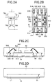
- a circuit device 53 of Fig. 2 will be described below.
- This circuit device has substantially the same structure as that of Fig. 1, except that the interconnects L1 and L2 are formed as the conductive paths 51. Accordingly, the interconnects L1 and L2 will be described below.
- IC circuits As described before, there are a wide variety of IC circuits from a small-scale circuit to a large-scale circuit.
- the small-scale circuit is only shown in Fig. 2A.
- This circuit is most applicable to an audio amplifying circuit having a difference amplifying circuit and a current mirror circuit connected.
- the difference amplifying circuit is constituted of a TR1 and a TR2
- the current mirror circuit is constituted of a TR3 and a TR4, as shown in Fig. 2A.
- Fig. 2B is a plan view of the circuit device to which the circuit of Fig. 2A is applied.
- Fig. 2C is a cross-sectional view taken along the line A-A in Fig. 2B.
- Fig. 2D is a cross-sectional view taken along the line B-B.
- a die pad 51A for mounting the TR1 and TR3 is provided to the left of Fig. 2B.
- a die pad 51D for mounting the TR2 and TR4 is provided.
- On the upper side of the die pads 51A, 51D there are provided the electrodes for external connection 51B, 51E to 51G, and on the lower side thereof, there are provided the electrodes for external connection 51C, 51H to 51J.
- an interconnect L2 is formed integrally with the electrodes 51E, 51G. Also, since a TR3 base and a TR4 base, as well as a TR3 emitter and a TR4 emitter are commonly connected, an interconnect L1 is formed integrally with the electrodes 51C, 55J, and an interconnect L3 is formed integrally with the electrodes 55H, 55I.
- the present invention has a feature of the interconnects L1 to L3. They correspond to the interconnects 25 and 29 in Fig. 28. These interconnects are different depending on the degree of integration of this circuit device, and have the width as narrow as 25 ⁇ m or more. Note that this width of 25 ⁇ m is a numerical value taken when the wet etching is used. If the dry etching is used, its width can be narrower.
- a conductive path L1 constituting the interconnect L1 simply has the back face exposed, and has a lateral face of curved structure which is supported by the insulating resin 50.
- the interconnect is buried into the insulating resin 50.
- the wires can be prevented from slipping or warping, unlike the wires simply pasted on the support substrate as shown in Fig. 25.
- the lateral face of the first conductive path is a rough face with curved structure, and the visor is formed on the surface of the conductive path, there occurs an anchor effect to prevent the conductive path from slipping off the insulating resin, as will be understood from a manufacturing method hereinafter described.
- the electrodes 51B, 51C, 551E to 51J for external connection are buried into the insulating resin, as described previously. Therefore, even if an external force is applied via an external lead secured therein, the electrodes are unlikely to be peeled.
- a circuit device 56 of Fig. 8 will be described below.
- This circuit device has substantially the same structure of Fig. 1 or 2, except that a conductive coat 57 is formed on the surface of the conductive paths 51.
- the conductive coat 57 on the conductive paths will be mainly described below.
- a first feature is to provide the conductive coat 57 to prevent the circuit device or the conductive path 51 from warping.
- the circuit device due to a difference in thermal expansion coefficient between the insulating resin and the conductive path material (hereinafter referred to as a first material) the circuit device itself may be warped, or the conductive path curved or peeled. Since the thermal conductivity of the conductive paths 51 is superior to that of the insulating resin, the conductive paths 51 will rise in temperature more rapidly, and expand.
- a second material having a smaller thermal expansion coefficient than the first material is coated. Thereby, it is possible to prevent the curvature or exfoliation of the conductive paths, and the warpage of the circuit device.
- the second material is preferably Au, Ni or Pt.
- Cu has an expansion coefficient of Cu is 16.7x10⁻⁶ (10 to the minus 6th power), Au 14x10-6, Ni 12.8x10⁻⁶, and Pt 8.9x10⁻⁶. In this case, a plurality of layers may be formed.
- a second feature is to provide an anchor effect based on the second material.
- a visor 58 which is formed of the second material, is formed over the conductive path 51 to be buried into the insulating resin 50, bringing about the anchor effect to prevent the slippage of the conductive paths 51.
- the visor 58 can be formed by the conductive path itself.
- both the curved structure 59 and the visor 58 develops the double anchor effect to suppress the slippage of the conductive paths 51.
- the circuit device having a transistor chip 52A and a passive element 52B mounted.
- the present invention is also applicable to a circuit device which is constituted of one semiconductor device sealed therein, as shown in Figs. 21 and 22.
- Fig. 21 shows a circuit device 81 in which a face down element 80 such as a CSP is mounted.
- Fig. 22 shows a circuit device 83 in which the passive element 82 such as a chip resistor or chip capacitor is sealed.
- the bonding wire may be provided between two conductive paths and sealed therein. This is usable as a fuse.
- a sheet conductive foil 60 is prepared.
- This conductive foil 60 is composed of a material which is selected in consideration of the adhesive property to the brazing material, bonding property and plating property.
- the material may be Cu or Al as the main constituent, or an alloy of Fe-Ni. Further lamination plate of Cu and Al is applicable.
- the conductive foil is preferably about 10 ⁇ m to 300 ⁇ m thick in view of the etching that is performed later.
- a copper foil having a thickness of 70 ⁇ m (2 ounces) is used. However, the thickness may be fundamentally over 300 ⁇ m or less than 10 ⁇ m. It is sufficient that the trench 61 which has a smaller depth than the thickness of the conductive foil 60 may be formed, as will be described later.
- the sheet laminated conductive foil 60 is rolled in a desired width, and may be carried to each process as will be described later, or may be cut in a predetermined size, the cut conductive foils being carried to each process.
- a step of removing the conductive foil 60 except for at least a region which becomes the conductive paths 51, below a thickness of the conductive foil 60, a step of mounting the circuit elements 52 on the conductive paths 60, and a step of coating the insulating resin 50 in the trench 61 formed at the step of removing and the conductive foil 60 to seal the circuit elements.
- a photo-resist (PR) (etching resistant mask) is applied on the conductive foil 60 of Cu, and patterned to expose the conductive foil 60 excluding the region which becomes the conductive paths 51, as shown in Fig. 4. And etching is performed via the photo-resist PR, as shown in Fig. 5A.
- This manufacturing method has a feature that the wet etching or dry etching can be performed non-anisotropically by selecting the etching condition. Then the lateral face (side surface) is a rough face and curved. Note that the depth of the trench 61 formed by etching is about 50-70 ⁇ m.
- etchant may be ferric chloride or cupric chloride.
- the conductive foil may be dipped in this etchant, or this etchant may be showered.
- etching in the transversal direction is difficult to proceed directly under the photo-resist PR as the etching mask, but is gradually made in a deeper portion of the trench61 in the transversal direction.
- the size of aperture corresponding to its position is smaller with increased height, to taper inversely, resulting in the anchor structure.
- the etching proceeds in the depth direction, but is suppressed in the transversal direction, so that this anchor structure becomes remarkable.
- the orientation-dependent(anisotoropic) etching or non-anisotropic etching can be made.
- Cu can not be removed by reactive ion etching.
- Cu can be removed by sputtering.
- the orientation-dependent etching or non-anisotropic etching can be effected, depending on the sputtering or etching conditions .
- a conductive material which is resistant to the etching liquid may be selectively coated, instead of the photo-resist.
- this conductive material becomes an etching protective film, so that the trench can be etched without the use of the photo resist PR.
- the conductive materials may include Ag, Au, Pt, Pd or N. These corrosion resistant conductive materials have a feature of being readily available as the die pad or bonding pad.
- Ag can be bonded with Au and the brazing material.
- the thermocompression bonding of chip can be effected with the Ag on the conductive coat 51, or the chip can be fixed via the brazing material such as solder. Since the Au bonding wire can be bonded to the conductive coat of Ag, the wire bonding is allowed. Accordingly, there is provided a merit that these conductive coats can be directly utilized as the die pad and the bonding pad.
- the circuit elements 52 include the semiconductor device 52A such as a transistor, a diode and an IC chip, and the passive element 52B such as a chip capacitor and a chip resistor. Though being thick, a face down semiconductor device such as CSP or BGA can be mounted.
- the bare transistor chip 52A is die bonded to the conductive path 51A. Also, the emitter electrode and the conductive path 51B, as well the base electrode and the conductive path 51B, are connected via the bonding wire 55A which has been fixed by ball bonding with thermocompression, or wedge bonding with ultrasonic wave.
- the chip capacitor or the passive element 52B is fixed via the brazing material such as solder or the conductive paste 55B.
- the bonding pad 26 which is very small in size, is provided integrally with the conductive foil 60, as shown in Fig. 5. Hence, there is a merit that the energy of bonding tool can be transferred, with greater bonding ability.
- the bonding wire may be pull-cut. Then, since the bonding pad is integrated with the conductive foil 60, floating of the bonding pad can be suppressed, leading to better pull-cut ability.
- the resin materials include a thermosetting resin such as epoxy resin for which the transfer molding is suitable, and a thermoplastic resin such as polyimide resin and polyphenylene sulfide for which the injection molding is usable.
- the insulating resin applied on the surface of the conductive foil 60 is adjusted so as to cover the thickness of about 100 ⁇ m from the top of the bonding wire 55A. This thickness may be increased or decreased in consideration of the strength of the circuit device.
- a feature of this step is that the conductive foil 60, which becomes the conductive paths, serves as the support substrate up to being coated with the insulating resin 50.
- the support substrate 5 which is intrinsically not required is adopted to form the conductive paths 7 to 11, as shown in Fig. 26.
- the conductive foil 60 which becomes the support substrate is a necessary substance for the electrodes. Therefore, there is a merit that the operation can be effected by saving the material, with less cost.
- the trench 61 has a smaller depth than the thickness of the conductive foil. Therefore, the conductive foil is not separated individually into the conductive paths. Accordingly, it can be treated integrally as one sheet conductive foil 60. It has a feature of the easy operation of carrying or mounting it onto the mold, when molding the insulating resin.
- the insulating resin 50 is fitted into the trench 61 having the curved structure, there occurs the anchor effect in this region to prevent the insulating resin 50 from being peeled, and the conductive paths 51 from slipping off the insulating resin 50, the conductive paths 51 being separated at the later step.
- the silicone resin Before coating this insulating resin 50, the silicone resin may be potted to protect the semiconductor chip or the connecting part of bonding wire, for example.
- This step of removing can be effected by polishing, grinding, etching, or metal evaporation using a laser irradiation.
- the circuit device was cut about 30 ⁇ m thick over the entire surface by a polishing or grinding apparatus to expose the insulating resin 50 from the trench 61. This exposed face is indicated by the dot line in Fig. 7. As a result, each of the conductive paths 51 is about 40 ⁇ m thick.
- the conductive foil maybe subjected to wet etching over the entire surface thereof. Then, the conductive foil may be cut over the entire surface by the polishing or grinding apparatus to expose the insulating resin 50. Further conductive path 51 can be separated by only wet etching step.
- the conductive paths 51 are exposed from the insulating resin 50.
- the trench 61 is cut, resulting in the trench 54 as shown in Fig. 1 (see Fig. 7).
- a conductive material such as solder 5D may be applied onto the second conductive paths 51 exposed, as required, to complete the circuit device as shown in Fig. 1.
- the conductive coat may be formed ahead on the back face of the conductive foil of Fig. 3. In this case, the conductive coat may be selectively applied on the portion corresponding to the conductive path.
- the way of coating may be by plating.
- This conductive coat may be a material resistant to etching. When this conductive coat is adopted, the conductive paths 51 can be formed only by etching, without polishing.
- the transistor and the chip resistor are only mounted on the conductive foil 60, but may be arranged in a matrix of transistors and chip resistors, or a matrix of circuits as shown in Fig. 28.
- the matrix can be divided into individual units by using a dicing apparatus, as will be described later.
- the circuit device 56 of flat type can be fabricated in which the conductive paths 51 are buried into the insulating resin 50, and there is a common back face for the conductive paths 51 and the insulating resin 50.
- a feature of this manufacturing method is that the insulating resin 50 is utilized as the support substrate and can be separated into the individual conductive paths.
- the insulating resin 50 is required to have the conductive paths 51 buried therein. There is no need of having unnecessary support substrate 5, unlike the conventional manufacturing method of Fig. 26. Accordingly, it can be manufactured with the minimum amount of material, with less cost.
- the thickness of the insulating resin from the surface of the conductive paths 51 can be adjusted when the insulating resin is attached at the previous step. Accordingly, the thickness of the circuit device 56 can be increased or decreased, depending on the circuit element to be mounted.
- the conductive paths 51 having a thickness of 40 ⁇ m is buried into the insulating resin 50 having a thickness of 400 ⁇ m (see Fig. 1).
- the second embodiment is substantially the same as the first embodiment (Figs. 1 and 2), except that a second material 70 which serves as the visor is applied. The details are not described here.
- a laminated conductive foil 60 is prepared in which the second material 70 having a small etching rate is applied on the conductive foil 60 made of the first material, as shown in Fig. 9.
- Ni is applied on the Cu foil, Cu and Ni can be etched by ferric chloride or cupric chloride at a time, advantageously resulting in the formation of the visor 58 of Ni, due to a difference between etching rates.
- the bold line indicates the conductive coat 70 made of Ni, its film thickness being preferably about 1 to 10 ⁇ m. The larger film thickness of Ni can form the visor 58 more easily.
- the second material may cover the first material as well as the material for selective etching.
- the film made of the second material is firstly patterned to cover the formed area of the conductive paths 51. Then, with this film as a mask, the first material is etched so that the visor 58 can be formed.
- the second materials may include Al, Ag, Pd and Au (see Fig. 9).
- the photo-resist PR is formed on the Ni conductive coat 70, and patterned so that the Ni conductive coat 70 may be exposed except for the region which becomes the conductive paths 51, as shown in Fig. 10. Then, etching is performed with the photo-resist, as shown in Fig. 11.
- the visor 58 juts out as the etching proceeds, because the Ni conductive coat 70 has a slower etching rate than the conductive foil Cu 60.
- a method for manufacturing a circuit device in which the IC circuits having the conductive paths composed of a plurality of kinds of circuit elements, wires, die pads and bonding pads are arranged like a matrix and divided into individual IC circuits after sealing.
- Fig. 2 and particularly a cross-sectional view of Fig. 2C the structure will be described below. This manufacturing method is substantially the same as in the first embodiment and the second embodiment, and is simply described.
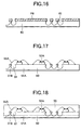
- a sheet conductive foil 60 is prepared, as shown in Fig. 14.
- the sheet conductive foil 60 is rolled in a predetermined width, and may be carried to the later process. Or the conductive foils cut in a predetermined size may be prepared and carried to the later process.
- the photo-resist PR is made on the Cu foil 60, and patterned so that the conductive foil 60 may be exposed except for the region which becomes the conductive paths 51, as shown in Fig. 15. And etching is performed via the photo-resist PR, as shown in Fig. 16.
- the trench 61 formed by etching is 50 ⁇ m in depth, for example, with its lateral face being rough, leading to increased adhesiveness of the insulating resin 50.
- the lateral face of the trench 61 is etched non-anisotropically, and curved.
- This step of removing can be wet etching, or dry etching.
- This curved structure produces the anchor effect. (For more details, refer to the first embodiment for the manufacturing method of the circuit device.)
- a conductive material which is resistant to the etching solution may be selectively coated, instead of the photo-resist PR. If it is selectively coated on the portion for the conductive paths, this conductive material serves as an etching protective film. As a result, the trench can be etched without the use of resist.
- the circuit elements 52A include semiconductor devices such as a transistor, a diode, and an IC chip, and passive elements such as a chip capacitor and a chip resistor. Also, though being thicker, the face down semiconductor devices such as CSP and BGA may be mounted.
- the bare transistor chip 52A is die bonded to the conductive path 51A. Consequently, the emitter electrode and the conductive path 51B, as well as the base electrode and the conductive path 51B are connected via the bonding wire 55A.
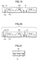
- a step of applying the insulating resin 50 to the conductive foil 60 and the trench 61 is shown in Fig. 18.
- This step can be performed by transfer molding, injection mold, or dipping.
- the insulating resin applied on the surface of the conductive foil 60 is adjusted to be about 100 ⁇ m thick from the top of the circuit elements mounted. This thickness can be made thicker or thinner in view of the strength of the circuit device.
- a feature of this step is that the conductive foil 60, which becomes the conductive paths 51, serves as the support substrate, when coated with the insulating resin 50.
- the support substrate 5 which is intrinsically not required is used to form the conductive paths 7 to 11, as shown in Fig. 26.
- the conductive foil 60 which becomes the support substrate is a necessary substance for the electrodes. As a result, the manufacturing operation can be performed by saving the material, with less cost.
- the trench 61 has a smaller depth than the thickness of the conductive foil. Therefore, the conductive foil is not separated individually into the conductive paths 51. Accordingly, it can be treated integrally as one sheet conductive foil 60. It has a feature of the easy operation of carrying or mounting it onto the mold, when molding the insulating resin.
- This step of removing can be effected by polishing, grinding, etching, or metal evaporation with laser.
- the circuit device was cut about 30 ⁇ m thick over the entire surface by a polishing or grinding apparatus to expose the insulating resin 50. This exposed face is indicated by the dot line in Fig. 18. As a result, each of the conductive paths 51 is about 40 ⁇ m thick.
- the conductive foil 60 may be subjected to wet etching over the entire surface thereof. Then, the conductive foil may be cut over the entire surface by the polishing or grinding apparatus to expose the insulating resin 50.
- a conductive material such as solder is applied on the exposed conductive paths 51, as shown in Fig. 19.
- the separation line is indicated by the arrow, and separation can be effected by dicing, cut, press, or chocolate break.
- separation can be effected by dicing, cut, press, or chocolate break.
- a projection on the mold may be provided to form the groove at the separation line in coating the insulating resin.
- the dicing is mostly used in the manufacturing method of the semiconductor devices, and is preferable because it can cut very small things.
- the manufacturing method as described in the first to third embodiments allows for the complex patterns, as shown in Fig. 28.
- the wire is bent and integral with the bonding pad 26, the other end being electrically connected with the circuit element.
- the wire is narrow in width, and long. Therefore, the warp(curvature) caused by heat is very significant, resulting in exfoliation in the conventional structure.
- the wires are buried into the insulating resin and supported, it is possible to prevent curvature, exfoliation and slippage of the wires.
- the bonding pad itself has a small plane area, and may be peeled in the conventional structure.
- the bonding pad is buried into the insulating resin and supported by the insulating resin, with the anchor effect, there is a merit of preventing the slippage.
- the circuit device having the circuit elements buried into the insulating resin 50 can be produced. This is similar to the conventional structure in which the circuit is incorporated into a printed circuit board or a ceramic substrate. This will be described later in connection with a way of mounting.
- the circuit device can be fabricated in accordance with the nine steps of preparing a Cu foil, plating with Ag or Ni, half etching, die bonding, wire bonding, transfer molding, removing the back face of Cu foil, treating the back face of conductive path, and dicing (dividing to a plurality of devices ) . And all the steps can be performed in the inside work without supplying the support substrate from the manufacturer.
- Fig. 21 shows a circuit device 81 having a face down circuit element 80 mounted.
- the circuit element 80 is a bare semiconductor chip which have solder ball in the face, CSP or BGA having sealed surface.
- Fig. 22 shows a circuit device 83 having a passive element 82 such as a chip resistor mounted. They are of thin type because of no need of the support substrate . Also, they are sealed by the insulating resin, and superior in the-environmental resistance.
- Fig. 23 shows the mounting structure.
- Fig. 23A shows the circuit devices 53, 81, and 83 as described above, which are mounted in the conductive paths 85 formed on a mounting substrate 84 such as a printed circuit board, metal substrate, or ceramic substrate.
- a conductive path 51A to which the back face of a semiconductor chip 52 is fixed is thermally coupled to the conductive paths 85 on the mounting substrate 84. Therefore, the heat of the circuit device can be radiated via the conductive paths 85. If the metal substrate is used for the mounting substrate 84, the temperature of the semiconductor chip 52 can be further decreased, due to radiation of the metal substrate. Therefore, the driving capability of the semiconductor chip can be enhanced. For example, the power MOS, IGBT, SIT, large current driving transistors, and large current driving IC (MOS, BIP, Bi-CMOS), memory IC are preferable.
- the metal substrates preferably include an Al substrate, a Cu substrate and a Fe substrate. In view of the short-circuit with the conductive paths 85, the insulating resin and/or oxide films are formed.
- Fig. 23B shows a circuit device 90 of the invention which is utilized as the substrate 84 of Fig. 23A.
- the conventional printed circuit board or ceramic substrate has a through hole TH formed in the substrate.
- a substrate module containing an IC circuit can be fabricated.
- at least one circuit (which may be contained as the system) is contained in the printed circuit board.
- the support substrate used the printed circuit board or ceramic substrate.
- the substrate module does not need the support substrate.
- This substrate module can be thinner and lighter than a hybrid substrate which may be the printed circuit board, the ceramic substrate, or the metal substrate.
- This circuit device 90 is utilized as the support substrate, and the circuit elements can be mounted in the exposed conductive paths, resulting in a high performance substrate module. Particularly, if this circuit device is a support substrate and a circuit device 91 is mounted on the support substrate, the substrate module can be made further thinner and lighter.
- an electronic apparatus with this module mounted can be reduced in size and weight.
- the hatching part indicated by numeral 93 is an insulating film.
- a high molecular film such as solder resist is preferable. Due to formation of this film, it is possible to prevent the conductive paths buried into the substrate 90 and the electrodes formed on the circuit elements 91 from short-circuiting.
- the semiconductor manufacturers fabricated the package type semiconductor devices and flip chips.
- the set makers mounted the semiconductor devices supplied from the semiconductor manufacturers and the passive elements supplied from the parts makers on the printed circuit board and incorporated the circuit devices into the set to fabricate an electronic apparatus.
- the circuit device of this invention allows itself to be used as the mounting substrate, the semiconductor manufacturers can complete the mounting substrate module in the later process, and deliver it to the set makers. Accordingly, the set makers can greatly save the operation of mounting the elements on the substrate.
- the present invention can fabricate the circuit devices with the conductive paths and the minimum amount of insulating resin, resulting in less wasteful resources. Hence, the circuit devices can be fabricated with less superfluous components up to completion, and with greatly reduced cost.
- the film thickness of insulating resin, and the thickness of conductive foil can be optimized, to make the circuit device smaller, thinner and lighter. Furthermore, since the wires liable to curvature or exfoliation are buried into the insulating resin, those problems can be resolved.
- the back face of conductive paths is exposed from the insulating resin, the back face of conductive paths can be directly contacted with the external. Hence, there is an advantage that the back face electrode and through hole of the conventional structure can be dispensed with.
- the heat developed by the circuit elements can be transferred directly via the conductive paths to the mounting substrate, because the back face of conductive paths is exposed.
- the power elements can be also mounted, due to this heat radiation.
- This circuit device has a flat plane structure in which the surface for the trench is substantially coincident with the surface for the conductive paths. If a narrow pitch QFP is mounted on the support substrate, the circuit device itself can be moved horizontally, as shown in Fig. 23B. Consequently, the lead shift can be easily modified.
- the second material is formed on the surface of the conductive paths, the warping of the mounting substrate, or particularly the curvature or exfoliation of the fine slender wire can be prevented.
- the conductive paths has the curved structure on the lateral face, and/or the second material is formed on the surface of conductive paths, a visor applied to a conductive path can be formed, bringing about the anchor effect to prevent the conductive paths from warping and slipping.
- the conductive foil itself serving as the conductive paths is utilized as the support substrate.
- the whole substrate is supported by the conductive foil, up to the steps of forming the trench or mounting the circuit elements and applying the insulating resin, while to divide the conductive foil into the conductive paths, the insulating resin is used as the support substrate.
- the circuit device of the invention can be manufactured with the least amount of circuit elements, conductive foil, and insulating resin, as required. As described in the conventional example, this circuit device can be fabricated without need of having the support substrate and with the reduced cost.
- the circuit device can be made very thin.
- the curved structure results, bringing about the anchor effect.
- the steps of forming the through hole and printing the conductors (for the ceramic substrate) can be omitted. Therefore, the manufacturing process can be significantly shortened, and advantageously the whole process can be performed in the inside work. Also, the frame mold is unnecessary at all, leading to quite short delivery.
- the conductive paths can be treated integrally, up to the step of removing the conductive foil (e.g., half etching), there is an advantage of the enhanced workability in the later step of coating the insulating resin.
- the circuit device mounted can be moved without impact upon the lateral face of the conductive paths on the mounting substrate. Particularly, the circuit device mismounted can be redisposed by shifting it horizontally. If the brazing material is molten after mouting the circuit device, the circuit device mismounted will tend to get back onto the conductive path, owing to surface tension of the molten brazing material. Consequently, the reallocation of circuit device can be effected by itself.
- this circuit device can be utilized as the support substrate to mount the circuit elements in the exposed conductive paths, resulting in a substrate module with high performance.
- this circuit device is used as the support substrate and the circuit device 91 as the circuit element is mounted thereon, the substrate module can be made lighter and thinner.
Landscapes
- Engineering & Computer Science (AREA)
- Microelectronics & Electronic Packaging (AREA)
- Manufacturing & Machinery (AREA)
- Lead Frames For Integrated Circuits (AREA)
- Structures Or Materials For Encapsulating Or Coating Semiconductor Devices Or Solid State Devices (AREA)
- Manufacturing Of Printed Wiring (AREA)
Applications Claiming Priority (8)
| Application Number | Priority Date | Filing Date | Title |
|---|---|---|---|
| JP2000022646 | 2000-01-31 | ||
| JP2000022646A JP3574025B2 (ja) | 2000-01-31 | 2000-01-31 | 回路装置およびその製造方法 |
| JP2000024047 | 2000-02-01 | ||
| JP2000024047A JP3574026B2 (ja) | 2000-02-01 | 2000-02-01 | 回路装置およびその製造方法 |
| JP2000032454A JP2001223318A (ja) | 2000-02-09 | 2000-02-09 | 回路装置およびその製造方法 |
| JP2000032417A JP3691328B2 (ja) | 2000-02-09 | 2000-02-09 | 回路装置および回路モジュール |
| JP2000032417 | 2000-02-09 | ||
| JP2000032454 | 2000-02-09 |
Publications (2)
| Publication Number | Publication Date |
|---|---|
| EP1122778A2 true EP1122778A2 (fr) | 2001-08-08 |
| EP1122778A3 EP1122778A3 (fr) | 2004-04-07 |
Family
ID=27480977
Family Applications (1)
| Application Number | Title | Priority Date | Filing Date |
|---|---|---|---|
| EP00308477A Withdrawn EP1122778A3 (fr) | 2000-01-31 | 2000-09-27 | Dispositif de circuit et son procédé de fabrication |
Country Status (5)
| Country | Link |
|---|---|
| US (3) | US6548328B1 (fr) |
| EP (1) | EP1122778A3 (fr) |
| KR (2) | KR100484696B1 (fr) |
| CN (1) | CN1246901C (fr) |
| TW (1) | TW535462B (fr) |
Cited By (5)
| Publication number | Priority date | Publication date | Assignee | Title |
|---|---|---|---|---|
| WO2002097880A3 (fr) * | 2001-05-25 | 2003-09-25 | Eupec Gmbh & Co Kg | Module a semi-conducteur de puissance et procede pour produire un module a semi-conducteur de puissance |
| EP1122988A3 (fr) * | 2000-01-28 | 2004-03-24 | Sanyo Electric Co., Ltd. | Carte de circuit, méthode de fabriquer la même chose et méthode de monter un élément électronique de circuit |
| WO2004077559A1 (fr) * | 2003-02-27 | 2004-09-10 | Infineon Technologies Ag | Boitier pour circuit integre, procede de production de ce dernier |
| EP1351295A3 (fr) * | 2002-03-21 | 2006-08-16 | Texas Instruments Incorporated | Cadres de connection prémétallisés, estampés, miniatures, sans plomb ayant des profiles gravés |
| EP2500954A4 (fr) * | 2009-11-12 | 2015-11-04 | Denki Kagaku Kogyo Kk | Substrat de support pour un élément émetteur de lumière et son procédé de production |
Families Citing this family (97)
| Publication number | Priority date | Publication date | Assignee | Title |
|---|---|---|---|---|
| JP3650008B2 (ja) * | 2000-09-04 | 2005-05-18 | 三洋電機株式会社 | Mosfetを用いた保護回路装置およびその製造方法 |
| TW511422B (en) * | 2000-10-02 | 2002-11-21 | Sanyo Electric Co | Method for manufacturing circuit device |
| US6712529B2 (en) * | 2000-12-11 | 2004-03-30 | Rohm Co., Ltd. | Infrared data communication module and method of making the same |
| JP2002184934A (ja) * | 2000-12-13 | 2002-06-28 | Shinko Electric Ind Co Ltd | 半導体装置及びその製造方法 |
| JP3609737B2 (ja) * | 2001-03-22 | 2005-01-12 | 三洋電機株式会社 | 回路装置の製造方法 |
| US6608375B2 (en) * | 2001-04-06 | 2003-08-19 | Oki Electric Industry Co., Ltd. | Semiconductor apparatus with decoupling capacitor |
| JP4034073B2 (ja) * | 2001-05-11 | 2008-01-16 | 株式会社ルネサステクノロジ | 半導体装置の製造方法 |
| JP2002368176A (ja) * | 2001-06-11 | 2002-12-20 | Rohm Co Ltd | 半導体電子部品のリードフレーム |
| KR20030019082A (ko) * | 2001-08-27 | 2003-03-06 | 산요 덴키 가부시키가이샤 | 회로 장치의 제조 방법 |
| JP4007798B2 (ja) * | 2001-11-15 | 2007-11-14 | 三洋電機株式会社 | 板状体の製造方法およびそれを用いた回路装置の製造方法 |
| US7190083B1 (en) * | 2002-01-07 | 2007-03-13 | Vixs Systems, Inc. | High frequency integrated circuit using capacitive bonding |
| US20040094826A1 (en) * | 2002-09-20 | 2004-05-20 | Yang Chin An | Leadframe pakaging apparatus and packaging method thereof |
| US20050012225A1 (en) * | 2002-11-15 | 2005-01-20 | Choi Seung-Yong | Wafer-level chip scale package and method for fabricating and using the same |
| JP2004207277A (ja) * | 2002-12-20 | 2004-07-22 | Sanyo Electric Co Ltd | 回路装置およびその製造方法 |
| JP2004214460A (ja) * | 2003-01-06 | 2004-07-29 | Sumitomo Electric Ind Ltd | 半導体装置 |
| CN100416815C (zh) * | 2003-02-21 | 2008-09-03 | 先进互连技术有限公司 | 包括无源器件的引线框架及其形成方法 |
| JP4245370B2 (ja) * | 2003-02-21 | 2009-03-25 | 大日本印刷株式会社 | 半導体装置の製造方法 |
| JP3954998B2 (ja) | 2003-08-11 | 2007-08-08 | ローム株式会社 | 半導体装置およびその製造方法 |
| JP2005129900A (ja) * | 2003-09-30 | 2005-05-19 | Sanyo Electric Co Ltd | 回路装置およびその製造方法 |
| EP1522521B1 (fr) * | 2003-10-10 | 2015-12-09 | Infineon Technologies AG | Capteur capacitif |
| US7122406B1 (en) * | 2004-01-02 | 2006-10-17 | Gem Services, Inc. | Semiconductor device package diepad having features formed by electroplating |
| US7145234B2 (en) * | 2004-01-15 | 2006-12-05 | Via Technologies, Inc. | Circuit carrier and package structure thereof |
| US7317742B2 (en) * | 2004-02-19 | 2008-01-08 | Sumitomo Electric Industries, Ltd. | Optical sub-assembly having a thermo-electric cooler and an optical transceiver using the optical sub-assembly |
| JP4446772B2 (ja) * | 2004-03-24 | 2010-04-07 | 三洋電機株式会社 | 回路装置およびその製造方法 |
| TWI227051B (en) * | 2004-04-09 | 2005-01-21 | Airoha Tech Corp | Exposed pad module integrated a passive device therein |
| CN100361293C (zh) * | 2004-04-28 | 2008-01-09 | 络达科技股份有限公司 | 内含无源元件的外露式有源元件基座模块 |
| JP4353853B2 (ja) * | 2004-05-20 | 2009-10-28 | 三洋電機株式会社 | 回路装置の製造方法および板状体 |
| US6940183B1 (en) * | 2004-06-04 | 2005-09-06 | Lu-Chen Hwan | Compound filled in lead IC packaging product |
| CN100555608C (zh) * | 2004-07-15 | 2009-10-28 | 大日本印刷株式会社 | 半导体装置与半导体装置制造用基板及它们的制造方法 |
| CN100466237C (zh) * | 2004-07-15 | 2009-03-04 | 大日本印刷株式会社 | 半导体装置与半导体装置制造用基板及该基板的制造方法 |
| US7413995B2 (en) * | 2004-08-23 | 2008-08-19 | Intel Corporation | Etched interposer for integrated circuit devices |
| US7348661B2 (en) * | 2004-09-24 | 2008-03-25 | Intel Corporation | Array capacitor apparatuses to filter input/output signal |
| US20060071351A1 (en) * | 2004-09-28 | 2006-04-06 | Texas Instruments Incorporated | Mold compound interlocking feature to improve semiconductor package strength |
| US7049208B2 (en) | 2004-10-11 | 2006-05-23 | Intel Corporation | Method of manufacturing of thin based substrate |
| US7358444B2 (en) * | 2004-10-13 | 2008-04-15 | Intel Corporation | Folded substrate with interposer package for integrated circuit devices |
| KR101182301B1 (ko) * | 2005-06-28 | 2012-09-20 | 엘지디스플레이 주식회사 | Led가 실장된 인쇄회로기판 |
| US7495330B2 (en) * | 2005-06-30 | 2009-02-24 | Intel Corporation | Substrate connector for integrated circuit devices |
| DE102005041064B4 (de) * | 2005-08-30 | 2023-01-19 | OSRAM Opto Semiconductors Gesellschaft mit beschränkter Haftung | Oberflächenmontierbares optoelektronisches Bauelement und Verfahren zu dessen Herstellung |
| JP2007157940A (ja) * | 2005-12-02 | 2007-06-21 | Nichia Chem Ind Ltd | 発光装置および発光装置の製造方法 |
| JP5291864B2 (ja) * | 2006-02-21 | 2013-09-18 | ルネサスエレクトロニクス株式会社 | Dc/dcコンバータ用半導体装置の製造方法およびdc/dcコンバータ用半導体装置 |
| US7434310B2 (en) * | 2006-06-05 | 2008-10-14 | Motorola, Inc. | Process to reform a plastic packaged integrated circuit die |
| US7537965B2 (en) * | 2006-06-21 | 2009-05-26 | Delphi Technologies, Inc. | Manufacturing method for a leadless multi-chip electronic module |
| DE102006033023A1 (de) * | 2006-07-17 | 2008-01-24 | Robert Bosch Gmbh | Halbleiteranordnung und entsprechendes Herstellungsverfahren |
| US9281218B2 (en) * | 2006-08-30 | 2016-03-08 | United Test And Assembly Center Ltd. | Method of producing a semiconductor package |
| WO2008069260A1 (fr) * | 2006-11-30 | 2008-06-12 | Sanyo Electric Co., Ltd. | Carte de montage d'élément de circuit, composant de circuit utilisant celle-ci, et climatiseur |
| US7777310B2 (en) * | 2007-02-02 | 2010-08-17 | Stats Chippac Ltd. | Integrated circuit package system with integral inner lead and paddle |
| JP2008235401A (ja) | 2007-03-19 | 2008-10-02 | Spansion Llc | 半導体装置及びその製造方法 |
| JP5601751B2 (ja) * | 2007-04-26 | 2014-10-08 | スパンション エルエルシー | 半導体装置 |
| US7663204B2 (en) * | 2007-04-27 | 2010-02-16 | Powertech Technology Inc. | Substrate for multi-chip stacking, multi-chip stack package utilizing the substrate and its applications |
| US8492883B2 (en) * | 2008-03-14 | 2013-07-23 | Advanced Semiconductor Engineering, Inc. | Semiconductor package having a cavity structure |
| DE102008024704A1 (de) * | 2008-04-17 | 2009-10-29 | Osram Opto Semiconductors Gmbh | Optoelektronisches Bauteil und Verfahren zur Herstellung eines optoelektronischen Bauteils |
| EP2133915A1 (fr) * | 2008-06-09 | 2009-12-16 | Micronas GmbH | Agencement semi-conducteur doté de conduites de liaison moulées de manière particulière et procédé de fabrication d'un tel agencement |
| US7829984B2 (en) * | 2008-06-25 | 2010-11-09 | Stats Chippac Ltd. | Integrated circuit package system stackable devices |
| US20100044850A1 (en) * | 2008-08-21 | 2010-02-25 | Advanced Semiconductor Engineering, Inc. | Advanced quad flat non-leaded package structure and manufacturing method thereof |
| TWI372454B (en) * | 2008-12-09 | 2012-09-11 | Advanced Semiconductor Eng | Quad flat non-leaded package and manufacturing method thereof |
| MY163911A (en) * | 2009-03-06 | 2017-11-15 | Shenzhen Standarad Patent & Trademark Agent Ltd | Leadless integrated circuit package having high density contacts |
| WO2010111885A1 (fr) | 2009-04-03 | 2010-10-07 | Kaixin, Inc. | Grille de connexion pour un boîtier de ci et son procédé de fabrication |
| US8124447B2 (en) | 2009-04-10 | 2012-02-28 | Advanced Semiconductor Engineering, Inc. | Manufacturing method of advanced quad flat non-leaded package |
| US20100314728A1 (en) * | 2009-06-16 | 2010-12-16 | Tung Lok Li | Ic package having an inductor etched into a leadframe thereof |
| KR101668141B1 (ko) | 2009-09-02 | 2016-10-20 | 카이씬, 인코포레이티드 | Ic 패키지 및 이의 제조방법 |
| US8749074B2 (en) * | 2009-11-30 | 2014-06-10 | Micron Technology, Inc. | Package including an interposer having at least one topological feature |
| US20110163430A1 (en) * | 2010-01-06 | 2011-07-07 | Advanced Semiconductor Engineering, Inc. | Leadframe Structure, Advanced Quad Flat No Lead Package Structure Using the Same, and Manufacturing Methods Thereof |
| EP2533616A4 (fr) * | 2010-02-01 | 2016-08-10 | Furukawa Electric Co Ltd | Substrat à âme métallique pour boîte de jonction électrique dans un véhicule |
| JP5711472B2 (ja) * | 2010-06-09 | 2015-04-30 | 新光電気工業株式会社 | 配線基板及びその製造方法並びに半導体装置 |
| US8519525B2 (en) * | 2010-07-29 | 2013-08-27 | Alpha & Omega Semiconductor, Inc. | Semiconductor encapsulation and method thereof |
| JP5242644B2 (ja) * | 2010-08-31 | 2013-07-24 | 株式会社東芝 | 半導体記憶装置 |
| WO2012036281A1 (fr) * | 2010-09-17 | 2012-03-22 | ローム株式会社 | Dispositif d'émission de lumière à semi-conducteurs, procédé pour sa production et dispositif d'affichage |
| TWI419290B (zh) | 2010-10-29 | 2013-12-11 | 日月光半導體製造股份有限公司 | 四方扁平無引腳封裝及其製作方法 |
| US8377750B2 (en) * | 2010-12-14 | 2013-02-19 | Stats Chippac Ltd. | Integrated circuit packaging system with multiple row leads and method of manufacture thereof |
| JP2012146963A (ja) * | 2010-12-20 | 2012-08-02 | Shinko Electric Ind Co Ltd | 半導体パッケージの製造方法及び半導体パッケージ |
| JP5582040B2 (ja) * | 2011-01-12 | 2014-09-03 | 富士電機株式会社 | 半導体装置の製造方法、半導体装置およびイグナイタ装置 |
| US8502363B2 (en) * | 2011-07-06 | 2013-08-06 | Advanced Semiconductor Engineering, Inc. | Semiconductor device packages with solder joint enhancement element and related methods |
| TWI508241B (zh) * | 2011-10-20 | 2015-11-11 | 先進封裝技術私人有限公司 | 封裝基板、封裝基板製程、半導體元件之封裝結構及其製程 |
| US8674487B2 (en) | 2012-03-15 | 2014-03-18 | Advanced Semiconductor Engineering, Inc. | Semiconductor packages with lead extensions and related methods |
| US9653656B2 (en) | 2012-03-16 | 2017-05-16 | Advanced Semiconductor Engineering, Inc. | LED packages and related methods |
| KR20140050387A (ko) * | 2012-10-19 | 2014-04-29 | 삼성테크윈 주식회사 | 반도체 패키지용 리이드 프레임과, 이를 제조하는 방법 |
| US9059379B2 (en) | 2012-10-29 | 2015-06-16 | Advanced Semiconductor Engineering, Inc. | Light-emitting semiconductor packages and related methods |
| CN103794574B (zh) * | 2012-10-31 | 2018-06-01 | 三垦电气株式会社 | 半导体装置及其制造方法 |
| JP6171402B2 (ja) * | 2013-03-01 | 2017-08-02 | セイコーエプソン株式会社 | モジュール、電子機器、および移動体 |
| US9087777B2 (en) * | 2013-03-14 | 2015-07-21 | United Test And Assembly Center Ltd. | Semiconductor packages and methods of packaging semiconductor devices |
| JP6352009B2 (ja) * | 2013-04-16 | 2018-07-04 | ローム株式会社 | 半導体装置 |
| CN105684000B (zh) * | 2013-10-22 | 2019-03-15 | 凸版印刷株式会社 | Ic模块以及ic卡、ic模块基板 |
| KR20150074649A (ko) * | 2013-12-24 | 2015-07-02 | 삼성전기주식회사 | 반도체 패키지 및 그 제조 방법 |
| JP2015144188A (ja) * | 2014-01-31 | 2015-08-06 | 株式会社東芝 | 半導体装置及びその製造方法 |
| GB2525585B (en) * | 2014-03-20 | 2018-10-03 | Micross Components Ltd | Leadless chip carrier |
| CN104320925B (zh) * | 2014-10-23 | 2018-01-19 | 安捷利(番禺)电子实业有限公司 | 一种新型埋入式电路板的制作方法 |
| US9570381B2 (en) | 2015-04-02 | 2017-02-14 | Advanced Semiconductor Engineering, Inc. | Semiconductor packages and related manufacturing methods |
| JP6555927B2 (ja) * | 2015-05-18 | 2019-08-07 | 大口マテリアル株式会社 | 半導体素子搭載用リードフレーム及び半導体装置の製造方法 |
| CN105097571B (zh) * | 2015-06-11 | 2018-05-01 | 合肥矽迈微电子科技有限公司 | 芯片封装方法及封装组件 |
| KR102479946B1 (ko) * | 2016-04-06 | 2022-12-22 | 해성디에스 주식회사 | 반도체 패키지 기판 및 그 제조방법 |
| JP6777365B2 (ja) * | 2016-12-09 | 2020-10-28 | 大口マテリアル株式会社 | リードフレーム |
| JP2018098487A (ja) * | 2016-12-14 | 2018-06-21 | 株式会社村田製作所 | 半導体モジュール |
| US11329030B2 (en) | 2017-05-02 | 2022-05-10 | Osram Opto Semiconductors Gmbh | Production of a chip module |
| TWM555065U (zh) * | 2017-09-05 | 2018-02-01 | 恆勁科技股份有限公司 | 電子封裝件及其封裝基板 |
| US10439065B2 (en) | 2017-10-11 | 2019-10-08 | Texas Instruments Incorporated | Inverted leads for packaged isolation devices |
| US10615105B2 (en) * | 2017-10-20 | 2020-04-07 | Advanced Semiconductor Engineering, Inc. | Semiconductor device package and method of manufacturing the same |
| US11393774B2 (en) * | 2019-08-21 | 2022-07-19 | Stmicroelectronics, Inc. | Semiconductor device having cavities at an interface of an encapsulant and a die pad or leads |
Citations (4)
| Publication number | Priority date | Publication date | Assignee | Title |
|---|---|---|---|---|
| JPH03240260A (ja) | 1990-02-19 | 1991-10-25 | Matsushita Electric Ind Co Ltd | 集積回路装置の製造方法 |
| JPH10313082A (ja) | 1997-03-10 | 1998-11-24 | Sanyo Electric Co Ltd | 半導体装置とその製造方法 |
| JPH11195733A (ja) | 1997-10-28 | 1999-07-21 | Seiko Epson Corp | 半導体装置の製造方法、半導体装置用導電性板および半導体装置 |
| US6001671A (en) | 1996-04-18 | 1999-12-14 | Tessera, Inc. | Methods for manufacturing a semiconductor package having a sacrificial layer |
Family Cites Families (30)
| Publication number | Priority date | Publication date | Assignee | Title |
|---|---|---|---|---|
| JPS5151281A (fr) * | 1974-10-31 | 1976-05-06 | Tokyo Shibaura Electric Co | |
| JPS59208756A (ja) * | 1983-05-12 | 1984-11-27 | Sony Corp | 半導体装置のパツケ−ジの製造方法 |
| US5122860A (en) * | 1987-08-26 | 1992-06-16 | Matsushita Electric Industrial Co., Ltd. | Integrated circuit device and manufacturing method thereof |
| DE68927295T2 (de) * | 1988-07-08 | 1997-05-07 | Oki Electric Ind Co Ltd | Kunstharzversiegeltes halbleiterbauelement |
| JPH02240940A (ja) * | 1989-03-15 | 1990-09-25 | Matsushita Electric Ind Co Ltd | 集積回路装置の製造方法 |
| JP2781018B2 (ja) | 1989-09-06 | 1998-07-30 | 新光電気工業株式会社 | 半導体装置およびその製造方法 |
| US5200362A (en) * | 1989-09-06 | 1993-04-06 | Motorola, Inc. | Method of attaching conductive traces to an encapsulated semiconductor die using a removable transfer film |
| US5216278A (en) * | 1990-12-04 | 1993-06-01 | Motorola, Inc. | Semiconductor device having a pad array carrier package |
| JP2532352B2 (ja) | 1992-05-25 | 1996-09-11 | マンネスマン・アクチエンゲゼルシャフト | 流体により冷却される出力トランジスタ装置 |
| JPH06244355A (ja) * | 1993-02-15 | 1994-09-02 | Tetsuya Hojo | リードフレームのピン保持固定部の形成方法、樹脂モールド時の樹脂漏れ防止部の形成方法、およびic等の放熱板固定部の形成方法 |
| EP0646962B1 (fr) * | 1993-04-14 | 2002-11-06 | Hitachi Construction Machinery Co., Ltd. | Procede d'usinage d'une feuille metallique, procede d'usinage d'une grille de connexion et procede d'usinage d'un dispositif a semi-conducteur |
| EP1213754A3 (fr) | 1994-03-18 | 2005-05-25 | Hitachi Chemical Co., Ltd. | Méthode de fabrication d'un boítier semi-conducteur et boítier semi-conducteur |
| JPH08115989A (ja) * | 1994-08-24 | 1996-05-07 | Fujitsu Ltd | 半導体装置及びその製造方法 |
| US5656550A (en) | 1994-08-24 | 1997-08-12 | Fujitsu Limited | Method of producing a semicondutor device having a lead portion with outer connecting terminal |
| JP3269745B2 (ja) | 1995-01-17 | 2002-04-02 | 株式会社日立製作所 | モジュール型半導体装置 |
| US5841190A (en) | 1995-05-19 | 1998-11-24 | Ibiden Co., Ltd. | High density multi-layered printed wiring board, multi-chip carrier and semiconductor package |
| JP3304705B2 (ja) * | 1995-09-19 | 2002-07-22 | セイコーエプソン株式会社 | チップキャリアの製造方法 |
| JP3516789B2 (ja) * | 1995-11-15 | 2004-04-05 | 三菱電機株式会社 | 半導体パワーモジュール |
| JP3870301B2 (ja) * | 1996-06-11 | 2007-01-17 | ヤマハ株式会社 | 半導体装置の組立法、半導体装置及び半導体装置の連続組立システム |
| US5981314A (en) * | 1996-10-31 | 1999-11-09 | Amkor Technology, Inc. | Near chip size integrated circuit package |
| US5994166A (en) | 1997-03-10 | 1999-11-30 | Micron Technology, Inc. | Method of constructing stacked packages |
| CN100370602C (zh) * | 1997-04-30 | 2008-02-20 | 日立化成工业株式会社 | 半导体元件装配用基板及其制造方法和半导体器件 |
| JPH11195742A (ja) * | 1998-01-05 | 1999-07-21 | Matsushita Electron Corp | 半導体装置及びその製造方法とそれに用いるリードフレーム |
| US6222739B1 (en) | 1998-01-20 | 2001-04-24 | Viking Components | High-density computer module with stacked parallel-plane packaging |
| JPH11233684A (ja) * | 1998-02-17 | 1999-08-27 | Seiko Epson Corp | 半導体装置用基板、半導体装置及びその製造方法並びに電子機器 |
| US6137164A (en) | 1998-03-16 | 2000-10-24 | Texas Instruments Incorporated | Thin stacked integrated circuit device |
| JP2000022044A (ja) * | 1998-07-02 | 2000-01-21 | Mitsubishi Electric Corp | 半導体装置とその製造方法 |
| US6831352B1 (en) | 1998-10-22 | 2004-12-14 | Azimuth Industrial Company, Inc. | Semiconductor package for high frequency performance |
| US6451627B1 (en) * | 1999-09-07 | 2002-09-17 | Motorola, Inc. | Semiconductor device and process for manufacturing and packaging a semiconductor device |
| US6362525B1 (en) | 1999-11-09 | 2002-03-26 | Cypress Semiconductor Corp. | Circuit structure including a passive element formed within a grid array substrate and method for making the same |
-
2000
- 2000-09-27 EP EP00308477A patent/EP1122778A3/fr not_active Withdrawn
- 2000-09-27 US US09/671,135 patent/US6548328B1/en not_active Expired - Fee Related
-
2001
- 2001-01-15 TW TW090100830A patent/TW535462B/zh not_active IP Right Cessation
- 2001-01-18 KR KR10-2001-0002824A patent/KR100484696B1/ko not_active Expired - Fee Related
- 2001-01-31 CN CNB011165952A patent/CN1246901C/zh not_active Expired - Fee Related
-
2003
- 2003-02-24 US US10/372,414 patent/US7125798B2/en not_active Expired - Fee Related
-
2004
- 2004-07-28 KR KR10-2004-0059095A patent/KR100509136B1/ko not_active Expired - Fee Related
- 2004-08-13 US US10/918,105 patent/US20050056916A1/en not_active Abandoned
Patent Citations (4)
| Publication number | Priority date | Publication date | Assignee | Title |
|---|---|---|---|---|
| JPH03240260A (ja) | 1990-02-19 | 1991-10-25 | Matsushita Electric Ind Co Ltd | 集積回路装置の製造方法 |
| US6001671A (en) | 1996-04-18 | 1999-12-14 | Tessera, Inc. | Methods for manufacturing a semiconductor package having a sacrificial layer |
| JPH10313082A (ja) | 1997-03-10 | 1998-11-24 | Sanyo Electric Co Ltd | 半導体装置とその製造方法 |
| JPH11195733A (ja) | 1997-10-28 | 1999-07-21 | Seiko Epson Corp | 半導体装置の製造方法、半導体装置用導電性板および半導体装置 |
Cited By (6)
| Publication number | Priority date | Publication date | Assignee | Title |
|---|---|---|---|---|
| EP1122988A3 (fr) * | 2000-01-28 | 2004-03-24 | Sanyo Electric Co., Ltd. | Carte de circuit, méthode de fabriquer la même chose et méthode de monter un élément électronique de circuit |
| WO2002097880A3 (fr) * | 2001-05-25 | 2003-09-25 | Eupec Gmbh & Co Kg | Module a semi-conducteur de puissance et procede pour produire un module a semi-conducteur de puissance |
| EP1351295A3 (fr) * | 2002-03-21 | 2006-08-16 | Texas Instruments Incorporated | Cadres de connection prémétallisés, estampés, miniatures, sans plomb ayant des profiles gravés |
| WO2004077559A1 (fr) * | 2003-02-27 | 2004-09-10 | Infineon Technologies Ag | Boitier pour circuit integre, procede de production de ce dernier |
| US7635642B2 (en) | 2003-02-27 | 2009-12-22 | Infineon Technologies Ag | Integrated circuit package and method for producing it |
| EP2500954A4 (fr) * | 2009-11-12 | 2015-11-04 | Denki Kagaku Kogyo Kk | Substrat de support pour un élément émetteur de lumière et son procédé de production |
Also Published As
| Publication number | Publication date |
|---|---|
| KR20040072574A (ko) | 2004-08-18 |
| KR100484696B1 (ko) | 2005-04-22 |
| EP1122778A3 (fr) | 2004-04-07 |
| KR100509136B1 (ko) | 2005-08-22 |
| CN1246901C (zh) | 2006-03-22 |
| US20030151135A1 (en) | 2003-08-14 |
| CN1343086A (zh) | 2002-04-03 |
| KR20010078000A (ko) | 2001-08-20 |
| US6548328B1 (en) | 2003-04-15 |
| US7125798B2 (en) | 2006-10-24 |
| TW535462B (en) | 2003-06-01 |
| US20050056916A1 (en) | 2005-03-17 |
Similar Documents
| Publication | Publication Date | Title |
|---|---|---|
| US6548328B1 (en) | Circuit device and manufacturing method of circuit device | |
| US7091606B2 (en) | Circuit device and manufacturing method of circuit device and semiconductor module | |
| US6562660B1 (en) | Method of manufacturing the circuit device and circuit device | |
| JP3639514B2 (ja) | 回路装置の製造方法 | |
| US6791199B2 (en) | Heat radiating semiconductor device | |
| JP3574026B2 (ja) | 回路装置およびその製造方法 | |
| JP3609684B2 (ja) | 半導体装置およびその製造方法 | |
| JP3561683B2 (ja) | 回路装置の製造方法 | |
| JP3691335B2 (ja) | 回路装置の製造方法 | |
| JP3759572B2 (ja) | 半導体装置 | |
| JP3634709B2 (ja) | 半導体モジュール | |
| JP3574025B2 (ja) | 回路装置およびその製造方法 | |
| JP3668090B2 (ja) | 実装基板およびそれを用いた回路モジュール | |
| JP3510839B2 (ja) | 半導体装置およびその製造方法 | |
| JP3639495B2 (ja) | 回路装置の製造方法 | |
| JP3691328B2 (ja) | 回路装置および回路モジュール | |
| JP4443190B2 (ja) | 半導体装置の製造方法 | |
| KR20010103565A (ko) | 판형체, 리드 프레임 및 반도체 장치의 제조 방법 | |
| JP3778783B2 (ja) | 回路装置およびその製造方法 | |
| JP4748892B2 (ja) | 回路装置の製造方法 | |
| JP4036603B2 (ja) | 半導体装置およびその製造方法 | |
| JP2005175509A (ja) | 回路装置 | |
| JP2001250883A (ja) | 回路装置の製造方法 | |
| JP2002237545A (ja) | 回路装置の製造方法 | |
| JP2005150767A (ja) | 回路装置 |
Legal Events
| Date | Code | Title | Description |
|---|---|---|---|
| PUAI | Public reference made under article 153(3) epc to a published international application that has entered the european phase |
Free format text: ORIGINAL CODE: 0009012 |
|
| AK | Designated contracting states |
Kind code of ref document: A2 Designated state(s): AT BE CH CY DE DK ES FI FR GB GR IE IT LI LU MC NL PT SE |
|
| AX | Request for extension of the european patent |
Free format text: AL;LT;LV;MK;RO;SI |
|
| PUAL | Search report despatched |
Free format text: ORIGINAL CODE: 0009013 |
|
| AK | Designated contracting states |
Kind code of ref document: A3 Designated state(s): AT BE CH CY DE DK ES FI FR GB GR IE IT LI LU MC NL PT SE |
|
| AX | Request for extension of the european patent |
Extension state: AL LT LV MK RO SI |
|
| RIC1 | Information provided on ipc code assigned before grant |
Ipc: 7H 01L 21/48 B Ipc: 7H 01L 21/56 B Ipc: 7H 01L 23/31 A |
|
| 17P | Request for examination filed |
Effective date: 20040727 |
|
| AKX | Designation fees paid |
Designated state(s): DE FI FR GB NL |
|
| 17Q | First examination report despatched |
Effective date: 20081027 |
|
| STAA | Information on the status of an ep patent application or granted ep patent |
Free format text: STATUS: THE APPLICATION IS DEEMED TO BE WITHDRAWN |
|
| 18D | Application deemed to be withdrawn |
Effective date: 20120814 |