EP1122781A2 - Hochdicht-montiertes Element mit Klebefolie - Google Patents
Hochdicht-montiertes Element mit Klebefolie Download PDFInfo
- Publication number
- EP1122781A2 EP1122781A2 EP00308076A EP00308076A EP1122781A2 EP 1122781 A2 EP1122781 A2 EP 1122781A2 EP 00308076 A EP00308076 A EP 00308076A EP 00308076 A EP00308076 A EP 00308076A EP 1122781 A2 EP1122781 A2 EP 1122781A2
- Authority
- EP
- European Patent Office
- Prior art keywords
- wiring board
- semiconductor device
- conductive sections
- adhesive sheet
- electrode terminals
- Prior art date
- Legal status (The legal status is an assumption and is not a legal conclusion. Google has not performed a legal analysis and makes no representation as to the accuracy of the status listed.)
- Withdrawn
Links
Images

Classifications
-
- H—ELECTRICITY
- H05—ELECTRIC TECHNIQUES NOT OTHERWISE PROVIDED FOR
- H05K—PRINTED CIRCUITS; CASINGS OR CONSTRUCTIONAL DETAILS OF ELECTRIC APPARATUS; MANUFACTURE OF ASSEMBLAGES OF ELECTRICAL COMPONENTS
- H05K3/00—Apparatus or processes for manufacturing printed circuits
- H05K3/30—Assembling printed circuits with electric components, e.g. with resistors
- H05K3/32—Assembling printed circuits with electric components, e.g. with resistors electrically connecting electric components or wires to printed circuits
- H05K3/321—Assembling printed circuits with electric components, e.g. with resistors electrically connecting electric components or wires to printed circuits by conductive adhesives
-
- H—ELECTRICITY
- H10—SEMICONDUCTOR DEVICES; ELECTRIC SOLID-STATE DEVICES NOT OTHERWISE PROVIDED FOR
- H10W—GENERIC PACKAGES, INTERCONNECTIONS, CONNECTORS OR OTHER CONSTRUCTIONAL DETAILS OF DEVICES COVERED BY CLASS H10
- H10W40/00—Arrangements for thermal protection or thermal control
- H10W40/20—Arrangements for cooling
- H10W40/22—Arrangements for cooling characterised by their shape, e.g. having conical or cylindrical projections
- H10W40/226—Arrangements for cooling characterised by their shape, e.g. having conical or cylindrical projections characterised by projecting parts, e.g. fins to increase surface area
- H10W40/228—Arrangements for cooling characterised by their shape, e.g. having conical or cylindrical projections characterised by projecting parts, e.g. fins to increase surface area the projecting parts being wire-shaped or pin-shaped
-
- H—ELECTRICITY
- H10—SEMICONDUCTOR DEVICES; ELECTRIC SOLID-STATE DEVICES NOT OTHERWISE PROVIDED FOR
- H10W—GENERIC PACKAGES, INTERCONNECTIONS, CONNECTORS OR OTHER CONSTRUCTIONAL DETAILS OF DEVICES COVERED BY CLASS H10
- H10W70/00—Package substrates; Interposers; Redistribution layers [RDL]
- H10W70/60—Insulating or insulated package substrates; Interposers; Redistribution layers
- H10W70/62—Insulating or insulated package substrates; Interposers; Redistribution layers characterised by their interconnections
- H10W70/63—Vias, e.g. via plugs
- H10W70/635—Through-vias
-
- H—ELECTRICITY
- H05—ELECTRIC TECHNIQUES NOT OTHERWISE PROVIDED FOR
- H05K—PRINTED CIRCUITS; CASINGS OR CONSTRUCTIONAL DETAILS OF ELECTRIC APPARATUS; MANUFACTURE OF ASSEMBLAGES OF ELECTRICAL COMPONENTS
- H05K2201/00—Indexing scheme relating to printed circuits covered by H05K1/00
- H05K2201/09—Shape and layout
- H05K2201/09209—Shape and layout details of conductors
- H05K2201/095—Conductive through-holes or vias
- H05K2201/09581—Applying an insulating coating on the walls of holes
-
- H—ELECTRICITY
- H05—ELECTRIC TECHNIQUES NOT OTHERWISE PROVIDED FOR
- H05K—PRINTED CIRCUITS; CASINGS OR CONSTRUCTIONAL DETAILS OF ELECTRIC APPARATUS; MANUFACTURE OF ASSEMBLAGES OF ELECTRICAL COMPONENTS
- H05K2201/00—Indexing scheme relating to printed circuits covered by H05K1/00
- H05K2201/10—Details of components or other objects attached to or integrated in a printed circuit board
- H05K2201/10227—Other objects, e.g. metallic pieces
- H05K2201/10378—Interposers
-
- H—ELECTRICITY
- H05—ELECTRIC TECHNIQUES NOT OTHERWISE PROVIDED FOR
- H05K—PRINTED CIRCUITS; CASINGS OR CONSTRUCTIONAL DETAILS OF ELECTRIC APPARATUS; MANUFACTURE OF ASSEMBLAGES OF ELECTRICAL COMPONENTS
- H05K2201/00—Indexing scheme relating to printed circuits covered by H05K1/00
- H05K2201/10—Details of components or other objects attached to or integrated in a printed circuit board
- H05K2201/10613—Details of electrical connections of non-printed components, e.g. special leads
- H05K2201/10621—Components characterised by their electrical contacts
- H05K2201/10674—Flip chip
-
- H—ELECTRICITY
- H10—SEMICONDUCTOR DEVICES; ELECTRIC SOLID-STATE DEVICES NOT OTHERWISE PROVIDED FOR
- H10W—GENERIC PACKAGES, INTERCONNECTIONS, CONNECTORS OR OTHER CONSTRUCTIONAL DETAILS OF DEVICES COVERED BY CLASS H10
- H10W72/00—Interconnections or connectors in packages
- H10W72/30—Die-attach connectors
- H10W72/321—Structures or relative sizes of die-attach connectors
- H10W72/325—Die-attach connectors having a filler embedded in a matrix
-
- H—ELECTRICITY
- H10—SEMICONDUCTOR DEVICES; ELECTRIC SOLID-STATE DEVICES NOT OTHERWISE PROVIDED FOR
- H10W—GENERIC PACKAGES, INTERCONNECTIONS, CONNECTORS OR OTHER CONSTRUCTIONAL DETAILS OF DEVICES COVERED BY CLASS H10
- H10W72/00—Interconnections or connectors in packages
- H10W72/30—Die-attach connectors
- H10W72/351—Materials of die-attach connectors
-
- H—ELECTRICITY
- H10—SEMICONDUCTOR DEVICES; ELECTRIC SOLID-STATE DEVICES NOT OTHERWISE PROVIDED FOR
- H10W—GENERIC PACKAGES, INTERCONNECTIONS, CONNECTORS OR OTHER CONSTRUCTIONAL DETAILS OF DEVICES COVERED BY CLASS H10
- H10W72/00—Interconnections or connectors in packages
- H10W72/30—Die-attach connectors
- H10W72/351—Materials of die-attach connectors
- H10W72/352—Materials of die-attach connectors comprising metals or metalloids, e.g. solders
-
- H—ELECTRICITY
- H10—SEMICONDUCTOR DEVICES; ELECTRIC SOLID-STATE DEVICES NOT OTHERWISE PROVIDED FOR
- H10W—GENERIC PACKAGES, INTERCONNECTIONS, CONNECTORS OR OTHER CONSTRUCTIONAL DETAILS OF DEVICES COVERED BY CLASS H10
- H10W72/00—Interconnections or connectors in packages
- H10W72/30—Die-attach connectors
- H10W72/351—Materials of die-attach connectors
- H10W72/353—Materials of die-attach connectors not comprising solid metals or solid metalloids, e.g. ceramics
- H10W72/354—Materials of die-attach connectors not comprising solid metals or solid metalloids, e.g. ceramics comprising polymers
Definitions
- the present invention relates to a high-density mounted device, and more particularly, to a high-density mounted device in which an adhesive sheet is laid between a wiring board and a plurality of semiconductor devices to be mounted thereon.
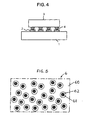
- FIG. 4 is a cross-sectional view showing a method of mounting a semiconductor device for use with a conventional high-density mounted device.
- reference numeral 1 designates a wiring board formed from glass epoxy or ceramic; 2 designates a plurality of electrode terminals provided on the primary surface of the wiring board; 3 designates a semiconductor device to be mounted on the wiring board 1; and 4 designates solder balls which are provided on respective un-illustrated electrode terminals of the semiconductor device 3 and arranged in what is commonly called a ball grid array (BGA).
- BGA ball grid array
- the semiconductor device 3 is mounted on the wiring board 1 by providing the solder balls 4 on the semiconductor device 3 so as to correspond to the respective electrode terminals 2 provided on the wiring board 1, attaching the solder balls 4 to solder paste which has been applied to the wiring board 1 beforehand, and fusing the solder balls 4 and the solder paste to thereby electrically and mechanically connect the solder balls 4 with the respective electrode terminals 2.
- a semiconductor device is electrically and mechanically connected to a wiring board through use of solder balls. Since the solder balls 4 are connected with the wiring board 1 by way of point contact, sufficient dissipation of heat developing in the semiconductor package has not been achieved.
- the present invention has been conceived to solve such a problem and is aimed at providing a high-density mounted device enabling sufficient electrical connection, sufficient heat dissipation, an improvement in grounding, and facilitated mounting of a high density mounted device.
- a high-density mounted device comprises a wiring board having a plurality of electrode terminals, and a (plurality of) semiconductor device(s) having a plurality of electrode terminals and mounted on the wiring board.
- An adhesive sheet is interposed between the wiring board and the semiconductor device, and the adhesive sheet includes a sheet-like adhesive base member and a plurality of conductive sections provided at predetermined pitches in the sheet-like adhesive base member.
- the conductive sections in the adhesive sheet extend from one side of the sheet-like adhesive base member to the other side thereof, and are electrically insulated from each other.
- the conductive sections enable electrical connection between the electrode terminals of the wiring board and the electrode terminals of the semiconductor device, and constitute heat conductive channels between the wiring board and the semiconductor device.
- the conductive sections in an adhesive sheet enable electrical connection between the ground terminals of the wiring board and the ground terminal(s) of the semiconductor device(s).
- FIGS. 1 and 2 A high-density mounted device according to a first embodiment of the present invention will now be described with reference to FIGS. 1 and 2.
- reference numeral 1 designates a wiring board formed from glass epoxy or ceramic; 2 designates a plurality of electrode terminals provided on the principal surface of the wiring board 1; 3 designates a semiconductor device to be mounted on the wiring board 1, such as a semiconductor element, semiconductor package, or module board; 5 designates a plurality of electrode terminals of the semiconductor device 3; and 6 designates an adhesive sheet to be interposed between the semiconductor device 3 and the wiring board 1.
- the adhesive sheet 6 has a structure such as that shown in FIG. 1.
- Reference numeral 60 designates an adhesive base member which constitutes the base of the adhesive sheet and is formed from adhesive thermo-plastic or like material; and 61 designates conductive sections which are provided in the base member 60 at predetermined intervals of, for example, 7 ⁇ m, and are made of metal such as copper.
- Each of the conductive sections 61 assumes a cylindrical shape which extends in a thicknesswise direction from one side of the base member 60 to the other side thereof.
- Reference numeral 62 designates a cylindrical insulation section which has a thickness of about 1 ⁇ m and surrounds the outer circumference of the cylindrical conductive section 61, thus serving as an insulation layer between conductive sections 61.
- the adhesive sheet 6 having the foregoing structure is interposed between the wiring board 1 and the semiconductor device 3.
- the wiring board 1 having the semiconductor device 3 mounted thereon is heated, and pressure is applied to the wiring board 1 in the direction in which the semiconductor device 3 is mounted on the wiring board 1, thereby integrally bonding together the adhesive sheet 6, the wiring board 1, and the semiconductor element 3.
- FIG. 2 only one conductive section 61 is shown between one electrode terminal 2 and its corresponding one electrode terminal 5.
- a plurality of conductive sections 61 are located between a pair of electrode terminals 2 and 5, thereby constituting a plurality of electrical and heat conducting channels. Therefore, the heat developed in the semiconductor device 3 can be sufficiently dissipated toward the wiring board 1.
- FIG. 3 is a cross-sectional view showing a structure of a high-density mounted device according to the second embodiment.
- reference numerals the same as those in FIGS. 1 and 2 designate like or corresponding elements, and repetition of their explanations is omitted.
- the high-density mounted device differs from that shown in FIG. 2 in that a ground terminal is provided on the surface of the wiring board 1 and the surface of the semiconductor device 3 in the same plane as that in which the electrode terminals 2 and 5 are provided and in that the ground terminal of the semiconductor device 3 and the ground terminal of the wiring board 1 are connected and grounded by way of the adhesive sheet 6.
- reference numeral 2G designates a ground terminal pattern formed on the wiring board 1. Since the ground terminal pattern 2G is formed by means of a plurality of terminals scattered and interconnected on the wiring board 1 where no electrode terminals 2 are present, the ground terminal pattern 2G is extended over a wide area and may assume a complicated pattern.
- Reference numeral 5G designates a ground terminal provided on the semiconductor device 3.
- the wiring board 1 and the semiconductor device 3, which have the foregoing structure, are integrally interconnected while the adhesive sheet 6 is interposed therebetween. Since a plurality of conductive sections 61 are provided in the sheet 6 at small intervals, the ground terminal pattern 2G can be connected to the ground terminal 5G of the semiconductor device 3 by means of the conductive sections 61 located in the positions corresponding to the ground terminal pattern 2G, even if the ground terminal pattern 2G assumes a complicated pattern.
- the semiconductor device 3 and the wiring board 1 can be sufficiently grounded. Further, even when the semiconductor device is a high-frequency circuit, the device can be prevented from becoming unstable or being susceptible to noise.
- the distribution is arbitrary, although neighboring conductive sections 61 should not touch each other.
- the intervals between conductive sections 61 may generally be less than 20 ⁇ m, preferably 5 - 10 ⁇ m.
- the material of the insulating sections 62 may be epoxy resin or poly-imide resin, for example, and may be the same as, or similar to, the material of the base member 60.
- the high-density mounted device has the foregoing structure, sufficient electrical and mechanical connection between a wiring board and a semiconductor device to be mounted thereon is achieved, and the heat developing in the semiconductor can be sufficiently dissipated by way of the wiring board.
- the adhesive sheet has an adhesive characteristic, a semiconductor device can be readily mounted on a wiring board by application of heat and pressure to the adhesive sheet.
- the ground terminal of the semiconductor device can be effectively connected to the ground pattern formed over a wide area of the wiring board, thus strengthening the grounding of the semiconductor device and the wiring board. Consequently, operation of the semiconductor device can be made stable and resistant to noise.
Landscapes
- Engineering & Computer Science (AREA)
- Manufacturing & Machinery (AREA)
- Microelectronics & Electronic Packaging (AREA)
- Cooling Or The Like Of Semiconductors Or Solid State Devices (AREA)
- Wire Bonding (AREA)
- Cooling Or The Like Of Electrical Apparatus (AREA)
- Structures For Mounting Electric Components On Printed Circuit Boards (AREA)
Applications Claiming Priority (2)
| Application Number | Priority Date | Filing Date | Title |
|---|---|---|---|
| JP2000023855A JP2001217279A (ja) | 2000-02-01 | 2000-02-01 | 高密度実装装置 |
| JP2000023855 | 2000-02-01 |
Publications (2)
| Publication Number | Publication Date |
|---|---|
| EP1122781A2 true EP1122781A2 (de) | 2001-08-08 |
| EP1122781A3 EP1122781A3 (de) | 2003-05-02 |
Family
ID=18549947
Family Applications (1)
| Application Number | Title | Priority Date | Filing Date |
|---|---|---|---|
| EP00308076A Withdrawn EP1122781A3 (de) | 2000-02-01 | 2000-09-18 | Hochdicht-montiertes Element mit Klebefolie |
Country Status (3)
| Country | Link |
|---|---|
| US (1) | US6411518B1 (de) |
| EP (1) | EP1122781A3 (de) |
| JP (1) | JP2001217279A (de) |
Families Citing this family (1)
| Publication number | Priority date | Publication date | Assignee | Title |
|---|---|---|---|---|
| US10141668B1 (en) * | 2017-07-06 | 2018-11-27 | Palo Alto Research Center Incorporated | Detachable flex-to-flex electrical connection |
Family Cites Families (23)
| Publication number | Priority date | Publication date | Assignee | Title |
|---|---|---|---|---|
| US4667219A (en) * | 1984-04-27 | 1987-05-19 | Trilogy Computer Development Partners, Ltd. | Semiconductor chip interface |
| JP2572570B2 (ja) | 1986-04-28 | 1997-01-16 | ダイソー株式会社 | ピンレスパッケージの実装方法 |
| US5283468A (en) * | 1988-05-30 | 1994-02-01 | Canon Kabushiki Kaisha | Electric circuit apparatus |
| US5068714A (en) * | 1989-04-05 | 1991-11-26 | Robert Bosch Gmbh | Method of electrically and mechanically connecting a semiconductor to a substrate using an electrically conductive tacky adhesive and the device so made |
| US5679977A (en) * | 1990-09-24 | 1997-10-21 | Tessera, Inc. | Semiconductor chip assemblies, methods of making same and components for same |
| EP0560072A3 (de) * | 1992-03-13 | 1993-10-06 | Nitto Denko Corporation | Anisotropisch-elektroleitende Klebe-Schicht und diese verwendende Verbindungsstruktur |
| US5371328A (en) * | 1993-08-20 | 1994-12-06 | International Business Machines Corporation | Component rework |
| US5543661A (en) * | 1994-05-31 | 1996-08-06 | Sumitomo Metal Ceramics Inc. | Semiconductor ceramic package with terminal vias |
| JPH08167630A (ja) * | 1994-12-15 | 1996-06-25 | Hitachi Ltd | チップ接続構造 |
| US5798909A (en) * | 1995-02-15 | 1998-08-25 | International Business Machines Corporation | Single-tiered organic chip carriers for wire bond-type chips |
| JP3004578B2 (ja) * | 1995-05-12 | 2000-01-31 | 財団法人工業技術研究院 | 熱放散増強のための多熱導伝路とパッケージ統合性及び信頼性向上のための縁の周りを囲むキャップからなる集積回路パッケージ |
| US5872338A (en) * | 1996-04-10 | 1999-02-16 | Prolinx Labs Corporation | Multilayer board having insulating isolation rings |
| US5808874A (en) * | 1996-05-02 | 1998-09-15 | Tessera, Inc. | Microelectronic connections with liquid conductive elements |
| US6022761A (en) * | 1996-05-28 | 2000-02-08 | Motorola, Inc. | Method for coupling substrates and structure |
| US5818700A (en) * | 1996-09-24 | 1998-10-06 | Texas Instruments Incorporated | Microelectronic assemblies including Z-axis conductive films |
| JPH10308565A (ja) * | 1997-05-02 | 1998-11-17 | Shinko Electric Ind Co Ltd | 配線基板 |
| US6008536A (en) * | 1997-06-23 | 1999-12-28 | Lsi Logic Corporation | Grid array device package including advanced heat transfer mechanisms |
| US5982630A (en) * | 1997-11-06 | 1999-11-09 | Intel Corporation | Printed circuit board that provides improved thermal dissipation |
| US6137164A (en) * | 1998-03-16 | 2000-10-24 | Texas Instruments Incorporated | Thin stacked integrated circuit device |
| US6258627B1 (en) * | 1999-01-19 | 2001-07-10 | International Business Machines Corporation | Underfill preform interposer for joining chip to substrate |
| US6191477B1 (en) * | 1999-02-17 | 2001-02-20 | Conexant Systems, Inc. | Leadless chip carrier design and structure |
| US6278181B1 (en) * | 1999-06-28 | 2001-08-21 | Advanced Micro Devices, Inc. | Stacked multi-chip modules using C4 interconnect technology having improved thermal management |
| AU2001242205A1 (en) * | 2000-03-31 | 2001-10-15 | Dyconex Patente Ag | Element and method for connecting constituents of an electronic assembly |
-
2000
- 2000-02-01 JP JP2000023855A patent/JP2001217279A/ja active Pending
- 2000-08-08 US US09/634,499 patent/US6411518B1/en not_active Expired - Fee Related
- 2000-09-18 EP EP00308076A patent/EP1122781A3/de not_active Withdrawn
Also Published As
| Publication number | Publication date |
|---|---|
| US6411518B1 (en) | 2002-06-25 |
| EP1122781A3 (de) | 2003-05-02 |
| JP2001217279A (ja) | 2001-08-10 |
Similar Documents
| Publication | Publication Date | Title |
|---|---|---|
| US6028358A (en) | Package for a semiconductor device and a semiconductor device | |
| US6225694B1 (en) | Semiconductor device | |
| US6501157B1 (en) | Substrate for accepting wire bonded or flip-chip components | |
| US6982494B2 (en) | Semiconductor device with signal line having decreased characteristic impedance | |
| KR100524437B1 (ko) | 반도체 장치, 반도체 장치용 기판 및 이들의 제조방법 및 전자기기 | |
| US5784258A (en) | Wiring board for supporting an array of imaging chips | |
| KR950024311A (ko) | 얇은 회로기판과 반도체 장치가 접합되어 있는 열전도성 지지부재를 갖춘 전자 패키지 | |
| JPH10242210A (ja) | 集積回路装置の実装構造およびその製造方法 | |
| EP0863549B1 (de) | Halbleiteranordnung mit einem Leitersubstrat | |
| CN102017135A (zh) | 带有在多个接触平面中的元器件的基板电路模块 | |
| US5151771A (en) | High lead count circuit board for connecting electronic components to an external circuit | |
| JP3164658B2 (ja) | 電子回路装置 | |
| US6034437A (en) | Semiconductor device having a matrix of bonding pads | |
| KR20010075680A (ko) | 접속된 접지면을 포함하는 전기 부품 및 전기 회로 모듈 | |
| JPH11163501A (ja) | 電子部品の実装方法、およびその方法によって製造された電子回路装置 | |
| KR970703617A (ko) | 전도선을 가진 리드프레임 리드를 포함한 고밀도 집적회로 조립체(a high density integrated circuit assembly combining leadframe leads with conductive traces) | |
| EP0817266B1 (de) | Montagestruktur für eine integrierte Schaltung | |
| US6512809B2 (en) | Radiation detector for an X-ray computed tomography apparatus | |
| US7439625B2 (en) | Circuit board | |
| US6101098A (en) | Structure and method for mounting an electric part | |
| US6208022B1 (en) | Electronic-circuit assembly | |
| US20050280018A1 (en) | Light-emitting diode | |
| JPH10303249A (ja) | 半導体装置 | |
| US6411518B1 (en) | High-density mounted device employing an adhesive sheet | |
| JP7192970B2 (ja) | 電子部品モジュール |
Legal Events
| Date | Code | Title | Description |
|---|---|---|---|
| PUAI | Public reference made under article 153(3) epc to a published international application that has entered the european phase |
Free format text: ORIGINAL CODE: 0009012 |
|
| AK | Designated contracting states |
Kind code of ref document: A2 Designated state(s): AT BE CH CY DE DK ES FI FR GB GR IE IT LI LU MC NL PT SE |
|
| AX | Request for extension of the european patent |
Free format text: AL;LT;LV;MK;RO;SI |
|
| PUAL | Search report despatched |
Free format text: ORIGINAL CODE: 0009013 |
|
| AK | Designated contracting states |
Designated state(s): AT BE CH CY DE DK ES FI FR GB GR IE IT LI LU MC NL PT SE |
|
| AX | Request for extension of the european patent |
Extension state: AL LT LV MK RO SI |
|
| AKX | Designation fees paid | ||
| REG | Reference to a national code |
Ref country code: DE Ref legal event code: 8566 |
|
| STAA | Information on the status of an ep patent application or granted ep patent |
Free format text: STATUS: THE APPLICATION IS DEEMED TO BE WITHDRAWN |
|
| 18D | Application deemed to be withdrawn |
Effective date: 20031104 |