EP1122786A2 - Hochleistungs-Multichip-IC-Gehäuse - Google Patents
Hochleistungs-Multichip-IC-Gehäuse Download PDFInfo
- Publication number
- EP1122786A2 EP1122786A2 EP01300535A EP01300535A EP1122786A2 EP 1122786 A2 EP1122786 A2 EP 1122786A2 EP 01300535 A EP01300535 A EP 01300535A EP 01300535 A EP01300535 A EP 01300535A EP 1122786 A2 EP1122786 A2 EP 1122786A2
- Authority
- EP
- European Patent Office
- Prior art keywords
- substrate
- chip
- package
- bonded
- flexible substrate
- Prior art date
- Legal status (The legal status is an assumption and is not a legal conclusion. Google has not performed a legal analysis and makes no representation as to the accuracy of the status listed.)
- Withdrawn
Links
Images
Classifications
-
- H—ELECTRICITY
- H10—SEMICONDUCTOR DEVICES; ELECTRIC SOLID-STATE DEVICES NOT OTHERWISE PROVIDED FOR
- H10W—GENERIC PACKAGES, INTERCONNECTIONS, CONNECTORS OR OTHER CONSTRUCTIONAL DETAILS OF DEVICES COVERED BY CLASS H10
- H10W72/00—Interconnections or connectors in packages
-
- H—ELECTRICITY
- H10—SEMICONDUCTOR DEVICES; ELECTRIC SOLID-STATE DEVICES NOT OTHERWISE PROVIDED FOR
- H10W—GENERIC PACKAGES, INTERCONNECTIONS, CONNECTORS OR OTHER CONSTRUCTIONAL DETAILS OF DEVICES COVERED BY CLASS H10
- H10W40/00—Arrangements for thermal protection or thermal control
- H10W40/10—Arrangements for heating
-
- H—ELECTRICITY
- H10—SEMICONDUCTOR DEVICES; ELECTRIC SOLID-STATE DEVICES NOT OTHERWISE PROVIDED FOR
- H10W—GENERIC PACKAGES, INTERCONNECTIONS, CONNECTORS OR OTHER CONSTRUCTIONAL DETAILS OF DEVICES COVERED BY CLASS H10
- H10W90/00—Package configurations
-
- H—ELECTRICITY
- H05—ELECTRIC TECHNIQUES NOT OTHERWISE PROVIDED FOR
- H05K—PRINTED CIRCUITS; CASINGS OR CONSTRUCTIONAL DETAILS OF ELECTRIC APPARATUS; MANUFACTURE OF ASSEMBLAGES OF ELECTRICAL COMPONENTS
- H05K1/00—Printed circuits
- H05K1/02—Details
- H05K1/14—Structural association of two or more printed circuits
- H05K1/141—One or more single auxiliary printed circuits mounted on a main printed circuit, e.g. modules, adapters
-
- H—ELECTRICITY
- H05—ELECTRIC TECHNIQUES NOT OTHERWISE PROVIDED FOR
- H05K—PRINTED CIRCUITS; CASINGS OR CONSTRUCTIONAL DETAILS OF ELECTRIC APPARATUS; MANUFACTURE OF ASSEMBLAGES OF ELECTRICAL COMPONENTS
- H05K1/00—Printed circuits
- H05K1/18—Printed circuits structurally associated with non-printed electric components
- H05K1/189—Printed circuits structurally associated with non-printed electric components characterised by the use of flexible or folded printed circuits
-
- H—ELECTRICITY
- H05—ELECTRIC TECHNIQUES NOT OTHERWISE PROVIDED FOR
- H05K—PRINTED CIRCUITS; CASINGS OR CONSTRUCTIONAL DETAILS OF ELECTRIC APPARATUS; MANUFACTURE OF ASSEMBLAGES OF ELECTRICAL COMPONENTS
- H05K3/00—Apparatus or processes for manufacturing printed circuits
- H05K3/30—Assembling printed circuits with electric components, e.g. with resistors
- H05K3/32—Assembling printed circuits with electric components, e.g. with resistors electrically connecting electric components or wires to printed circuits
- H05K3/34—Assembling printed circuits with electric components, e.g. with resistors electrically connecting electric components or wires to printed circuits by soldering
- H05K3/341—Surface mounted components
- H05K3/3431—Leadless components
- H05K3/3436—Leadless components having an array of bottom contacts, e.g. pad grid array or ball grid array components
-
- H—ELECTRICITY
- H10—SEMICONDUCTOR DEVICES; ELECTRIC SOLID-STATE DEVICES NOT OTHERWISE PROVIDED FOR
- H10W—GENERIC PACKAGES, INTERCONNECTIONS, CONNECTORS OR OTHER CONSTRUCTIONAL DETAILS OF DEVICES COVERED BY CLASS H10
- H10W90/00—Package configurations
- H10W90/701—Package configurations characterised by the relative positions of pads or connectors relative to package parts
- H10W90/721—Package configurations characterised by the relative positions of pads or connectors relative to package parts of bump connectors
- H10W90/724—Package configurations characterised by the relative positions of pads or connectors relative to package parts of bump connectors between a chip and a stacked insulating package substrate, interposer or RDL
Definitions
- This invention relates to flip chip integrated circuit (IC) packages and more specifically to multi-chip IC packages with high interconnect density.
- Multi-chip IC packages are becoming standard in the IC industry because of increased device packing density, which translates into smaller packages with reduced cost.
- Typical multi-chip packages have multiple chips or multi-chip modules carried by a printed wiring board.
- IC packages In an effort to increase device packing density, IC packages have been proposed and used with multiple chips mounted on both sides of a printed wiring board. This approach complicates the interconnection strategy in the overall assembly, but reduces by nearly one-half the footprint of the IC package.
- More recent developments in high density, low cost, IC packaging have taken advantage of flexible substrates which in some package designs allow more versatility for final assembly of the system. Flexible substrates are also used increasingly due to very fine, and thus dense, interconnection patterns. Also, flexible substrates permit simple through hole interconnections.
- Thin interconnect substrates that have through hole interconnections may be used to advantage to reduce the interconnection length between critical device components. Thinner substrates produce shorter interconnections.
- Thinner substrates produce shorter interconnections.
- the thin flexible substrate is provided with mechanical support by bonding the flexible substrate to a rigid support substrate, e.g., a metal sheet or a printed circuit board. Openings in the support substrate are provided to accommodate the IC chips on the side of the flexible substrate that is bonded to the rigid board. Interconnections between the logic and memory chips are made using vias, and the vias are exceptionally short due to the very thin flexible substrate. This arrangement also allows efficient heat sinking of the IC chips in the recessed portion of the rigid board by covering the recessed portion with a heat sink plate.
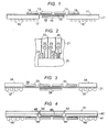
- a flexible substrate with IC chips mounted on both sides of the flexible substrate is shown in Fig. 1.
- the flexible substrate 11 carries a plurality of IC memory chips 13 bonded with solder bumps 14 to the top of the substrate.
- a logic IC chip 15 is bonded with solder bumps 16 to the underside of substrate 11.
- the flexible substrate has printed circuit interconnections (not shown for clarity) on both sides of the flexible substrate providing interconnections for the IC chips.
- the flexible substrate 11 is bonded to a support substrate 17 which may be any appropriate rigid board that has interconnection sites on both sides. In this embodiment, support substrate 17 is preferably a standard epoxy printed wiring board.
- the term rigid in the context of this prescription is intended to mean any board structure with rigidity greater than that of the flexible substrate 11.
- the support substrate 17 adds a second level of interconnection, and has through hole interconnections (not shown) for interconnecting the multiple chips 13 to the ball grid array (BGA) shown at 19.
- IC chip 15 is interconnected to the BGA by the printed circuit on the lower surface of the flexible substrate 11.
- the BGA is connected to the next board level.
- the advantage of having a large pitch at this level in the package is that support substrate 17 can be flip-bonded to a printed wiring board using large BGA solder bumps or balls. Large solder interconnections are very reliable and can be made with high yield.
- the solder bump sites on the IC chips 13 and 15 are normally provided with under bump metallization (UBM), which typically comprises solder wettable pads of e.g. Cu-Cr alloy or Ti-Pt-Au.
- UBM under bump metallization
- the solder bump sites on the flexible substrate 11 are preferably pads incorporated in the copper printed circuits and the solder bumps can be soldered directly to the copper pads.
- the support substrate 17 is provided with openings 18 to accommodate the IC chips mounted on the underside of the flexible substrate.
- Fig. 1 It is evident in the arrangement of Fig. 1 that the footprint of the IC chips mounted on the underside of the flexible substrate is constrained by the openings in the support substrate. However, typical expoxy printed wiring boards, e.g. FR4 boards, have sufficient structural integrity that a large percentage of the board area can be provided with openings such as opening 18. It is also evident from Fig. 1 that the number and arrangement of IC chips on the top surface of flexible substrate 11 is unconstrained.
- the IC array with the larger footprint will be mounted on the top side of the flexible substrate, where the footprint may exceed the area of the openings in the support substrate 17.
- the memory chips be mounted on one side of the flexible substrate, where interconnections between memory chips, especially the V DD and V SS busses, are conveniently accommodated, and the IC logic chips mounted on the other side of the flexible substrate.
- the memory chip array will typically be the larger array and thus mounted, in the arrangement of Fig. 1, on the side of the flexible substrate that is unconstrained, i.e. is not bonded to the support substrate.
- the interconnection density of the IC package of Fig. 1 can be very high since interconnection circuitry may be provided on both sides of the flexible substrate.
- a cutaway portion of the flexible substrate is shown in Fig. 2.
- Flexible substrate 21 is provided with through hole interconnections 23.
- Runners 25 provide interconnections between IC chips and shorter versions may provide interchip interconnections.
- a portion of an IC chip is shown at 26.
- the through hole interconnections may be for interconnections between IC chips on opposite sides of the flexible substrate, or may be for interconnections between the top side of the flexible substrate and the support substrate 17. It will be appreciated by those skilled in the art that elements in the figures described herein are not necessarily drawn to scale. The through holes and the printed circuits on the flexible substrate are typically very fine.
- the flexible substrate 31 carries the same IC chip contingent, i.e. memory IC chips 33 and logic chip 35, as in Fig. 1.
- the support substrate 34 with opening 36, is used in this embodiment mainly to provide rigidity, and interconnections on this support substrate are not required.
- the support substrate may be made from a variety of materials, e.g. epoxy FP4, or a thermally conductive material, e.g. Cu, Al.
- the preferred choice is copper, which has thermal expansion characteristics compatible with commonly used interconnect substrates.
- the BGA 37 for interconnecting the IC chips to the next level is solder bump bonded directly to flexible substrate 31. This embodiment allows a large area for routing on the lower side of the flexible substrate.
- FIG. 4 Another embodiment of the double sided flexible substrate assembly of the invention is shown in Fig. 4. This represents the preferred embodiment of the three shown.
- the flexible substrate 41 is bonded to support substrate 42.
- a memory IC chip array 44 is solder bump bonded to the lower side of the flexible substrate and one or more logic IC chips, represented by IC chip 46, are solder bump bonded to the upper side of the flexible substrate.
- the support substrate has opening 48 to accommodate IC chip 46.
- BGA 49 is bonded to the lower side of the flexible substrate as shown. Interconnections between the elements are implemented as described above.
- the thickness of the support substrate 41 is made to approximate the thickness of IC chip 46 plus the standoff due to the solder bump bonds for IC chip 46.
- IC chip 46 is a logic chip which typically has the largest number of lOs in the multiple IC chip assembly, and in many applications requires heat sinking to prevent overheating of the chip in operation.
- the heat sink 51 is typically a metal plate bonded to the backside of IC chip 46 and to the support substrate 42. The heat sink plate provides additional structural integrity for the package and may serve also as a cover for the assembly. Heat sink plate 51 may also be provided with holes 52 to allow underfill to be injected into the cavity 48, providing further package integrity and protection from hostile ambients. The underfill and the heat sink plate bonding operations may be combined for convenience, and use the same epoxy material.
- the support substrate 42 functions mainly as a standoff member or spacer, and accordingly can be combined with or integrated with the heat sink plate 51, e.g., elements 51 and 42 can be a single member. It will also be appreciated that the flexibility of flexible substrate 41 aids in creating intimate contact between the backside of IC chip 46 and the heat sink plate 51.
- Heat sink plate 51 may be formed of a heat conductive metal, e.g. copper or aluminum. In the preferred case the spacer/heat sink plate is copper.
- the multi-chip package of the invention offers the advantage of high interconnect density by flip-chip mounting IC chips on both sides of an interconnect substrate, and interconnecting the IC chips through the substrate with optimization of lead lengths resulting from the use of a very thin flexible substrate.
- the flexible substrate is a polymer, such as polyimide, with a thickness of less than 10 mils and preferably less than 4 mils.
- the printed circuit on each side of the flexible substrate preferably has a thickness in the range 0.5-2.0 mils.
- the flexible substrate has two interconnect levels.
- the flexible substrate may also have a multilevel interconnect structure with, e.g., two polymer sheets and four interconnect levels. Multilevel structures can be made with overall thickness less than 10 mils, which will provide suitable flexibility.
- the IC chips are typically thinned at the wafer level to approximately 6-20 mils, starting with, e.g., a 30 mil thick wafer.
- the IC chip thickness and the standoff typically 1-5 mils, result in an overall standoff between the flexible substrate surface and the backside of the IC chip of 7-25 mils.
- the support substrate 42 or alternatively the spacer elements in whatever form used, have a corresponding thickness to allow effective thermal contact with the IC chip backside.
- the vias through the flexible substrate will typically be 0.5 - 2.0 mils in diameter formed, e.g., by laser drilling.
- the flexibility of the flexible substrate described for this invention is a function of the substrate material and thickness.
- a polymer substrate with a thickness less than 10 mils and preferably less than 4 mils will generally afford the appropriate flexibility and the desired short through hole interconnections.
- Some aspects of the invention can be implemented with more standard substrates, e.g. printed wiring boards and ceramic substrates.
- substrates e.g. printed wiring boards and ceramic substrates.
- the placing memory chips on one side of a double sided support substrate and logic chips on the other, or of providing openings on one side of the board to accommodate IC chips in a recessed chip arrangement have advantages and valuable applications even when applied to ceramic substrates.
- the substrates in these cases may be thicker than 10 mils, e.g. up to 30 mils.
- Flip-chip bonding as used in connection with the invention is well known in the art and involves solder bump bonding of an IC chip to a substrate with the active side of the active chip facing the surface of the substrate.
- the space between the IC chip and the substrate, commonly referred to as standoff, may be filled with an epoxy underfill to impart robustness to the package and protect the active surface of the IC device from hostile environments.
Landscapes
- Structures For Mounting Electric Components On Printed Circuit Boards (AREA)
- Combinations Of Printed Boards (AREA)
- Cooling Or The Like Of Semiconductors Or Solid State Devices (AREA)
- Wire Bonding (AREA)
Applications Claiming Priority (2)
| Application Number | Priority Date | Filing Date | Title |
|---|---|---|---|
| US498005 | 2000-02-04 | ||
| US09/498,005 US6678167B1 (en) | 2000-02-04 | 2000-02-04 | High performance multi-chip IC package |
Publications (2)
| Publication Number | Publication Date |
|---|---|
| EP1122786A2 true EP1122786A2 (de) | 2001-08-08 |
| EP1122786A3 EP1122786A3 (de) | 2004-01-28 |
Family
ID=23979222
Family Applications (1)
| Application Number | Title | Priority Date | Filing Date |
|---|---|---|---|
| EP01300535A Withdrawn EP1122786A3 (de) | 2000-02-04 | 2001-01-22 | Hochleistungs-Multichip-IC-Gehäuse |
Country Status (6)
| Country | Link |
|---|---|
| US (1) | US6678167B1 (de) |
| EP (1) | EP1122786A3 (de) |
| JP (1) | JP2001244406A (de) |
| KR (1) | KR100742107B1 (de) |
| SG (1) | SG99346A1 (de) |
| TW (1) | TW516209B (de) |
Cited By (7)
| Publication number | Priority date | Publication date | Assignee | Title |
|---|---|---|---|---|
| DE10142116A1 (de) * | 2001-08-30 | 2002-11-14 | Infineon Technologies Ag | Elektronisches Bauteil und Verfahren zu seiner Herstellung |
| DE10142114C1 (de) * | 2001-08-30 | 2003-02-13 | Infineon Technologies Ag | Elektronisches Bauteil mit wenigstens zwei Halbleiterchips sowie Verfahren zu seiner Herstellung |
| WO2003058717A3 (en) * | 2001-12-28 | 2004-03-11 | Intel Corp | Package for a non-volatile memory device including integrated passive devices and method for making the same |
| WO2004107441A1 (en) * | 2003-05-28 | 2004-12-09 | Infineon Technologies Ag | An integrated circuit package employing a flexible substrate |
| EP1387403A3 (de) * | 2002-07-30 | 2006-05-24 | Kabushiki Kaisha Toshiba | Halbleitergehäuse |
| EP2135281A4 (de) * | 2007-03-29 | 2010-06-02 | Temic Automotive Na Inc | Thermische streuung bei chipsubstraten |
| DE112005003671B4 (de) * | 2005-08-31 | 2010-11-25 | Intel Corporation, Santa Clara | Baugruppe mit einem Mikroprozessor und einem Cache der Ebene L4 und Verfahren zur Herstellung der Baugruppe und System aufweisend die Baugruppe |
Families Citing this family (55)
| Publication number | Priority date | Publication date | Assignee | Title |
|---|---|---|---|---|
| US6627998B1 (en) * | 2000-07-27 | 2003-09-30 | International Business Machines Corporation | Wafer scale thin film package |
| JP2002305284A (ja) * | 2001-02-05 | 2002-10-18 | Mitsubishi Electric Corp | 半導体装置積層構造体 |
| US6856007B2 (en) * | 2001-08-28 | 2005-02-15 | Tessera, Inc. | High-frequency chip packages |
| US7176506B2 (en) * | 2001-08-28 | 2007-02-13 | Tessera, Inc. | High frequency chip packages with connecting elements |
| JP3093800U (ja) * | 2002-11-01 | 2003-05-16 | アルプス電気株式会社 | 電子ユニット |
| US7126210B2 (en) * | 2003-04-02 | 2006-10-24 | Stmicroelectronics, Inc. | System and method for venting pressure from an integrated circuit package sealed with a lid |
| JP2004311768A (ja) * | 2003-04-08 | 2004-11-04 | Shinko Electric Ind Co Ltd | 基板の製造方法及び半導体装置用基板及び半導体装置 |
| US6972480B2 (en) | 2003-06-16 | 2005-12-06 | Shellcase Ltd. | Methods and apparatus for packaging integrated circuit devices |
| WO2005004195A2 (en) * | 2003-07-03 | 2005-01-13 | Shellcase Ltd. | Method and apparatus for packaging integrated circuit devices |
| US20050067681A1 (en) * | 2003-09-26 | 2005-03-31 | Tessera, Inc. | Package having integral lens and wafer-scale fabrication method therefor |
| US7224056B2 (en) * | 2003-09-26 | 2007-05-29 | Tessera, Inc. | Back-face and edge interconnects for lidded package |
| US20050139984A1 (en) * | 2003-12-19 | 2005-06-30 | Tessera, Inc. | Package element and packaged chip having severable electrically conductive ties |
| WO2005086532A2 (en) * | 2004-03-01 | 2005-09-15 | Tessera, Inc. | Packaged acoustic and electromagnetic transducer chips |
| US20050224942A1 (en) * | 2004-03-26 | 2005-10-13 | Fan Ho | Semiconductor device with a plurality of ground planes |
| US20050230842A1 (en) * | 2004-04-20 | 2005-10-20 | Texas Instruments Incorporated | Multi-chip flip package with substrate for inter-die coupling |
| JP4738996B2 (ja) * | 2004-12-13 | 2011-08-03 | キヤノン株式会社 | 半導体装置 |
| US8143095B2 (en) * | 2005-03-22 | 2012-03-27 | Tessera, Inc. | Sequential fabrication of vertical conductive interconnects in capped chips |
| JP4590294B2 (ja) * | 2005-04-13 | 2010-12-01 | 株式会社リコー | 三次元成形回路部品の製造方法 |
| CN100403532C (zh) * | 2005-08-19 | 2008-07-16 | 南茂科技股份有限公司 | 散热型球格阵列封装结构 |
| JP2007123457A (ja) * | 2005-10-27 | 2007-05-17 | Nec Electronics Corp | 半導体モジュール |
| US7834276B2 (en) * | 2005-12-16 | 2010-11-16 | Unitech Printed Circuit Board Corp. | Structure for connecting a USB communication interface in a flash memory card by the height difference of a rigid flexible board |
| US7936062B2 (en) * | 2006-01-23 | 2011-05-03 | Tessera Technologies Ireland Limited | Wafer level chip packaging |
| US20070190747A1 (en) * | 2006-01-23 | 2007-08-16 | Tessera Technologies Hungary Kft. | Wafer level packaging to lidded chips |
| US20080002460A1 (en) * | 2006-03-01 | 2008-01-03 | Tessera, Inc. | Structure and method of making lidded chips |
| CN101480114A (zh) * | 2006-07-05 | 2009-07-08 | 富士通株式会社 | 印刷基板和印刷基板单元以及电子设备 |
| US8604605B2 (en) | 2007-01-05 | 2013-12-10 | Invensas Corp. | Microelectronic assembly with multi-layer support structure |
| US7981698B2 (en) * | 2007-03-09 | 2011-07-19 | The Charles Stark Draper Laboratory, Inc. | Removal of integrated circuits from packages |
| JP2008226945A (ja) * | 2007-03-09 | 2008-09-25 | Casio Comput Co Ltd | 半導体装置およびその製造方法 |
| JP2008251608A (ja) * | 2007-03-29 | 2008-10-16 | Casio Comput Co Ltd | 半導体装置およびその製造方法 |
| US8207607B2 (en) | 2007-12-14 | 2012-06-26 | Denso Corporation | Semiconductor device with resin mold |
| US7791175B2 (en) * | 2007-12-20 | 2010-09-07 | Mosaid Technologies Incorporated | Method for stacking serially-connected integrated circuits and multi-chip device made from same |
| US8399973B2 (en) * | 2007-12-20 | 2013-03-19 | Mosaid Technologies Incorporated | Data storage and stackable configurations |
| US8358155B2 (en) * | 2008-01-29 | 2013-01-22 | Oracle America, Inc. | Circuit that facilitates proximity communication |
| US7863732B2 (en) * | 2008-03-18 | 2011-01-04 | Stats Chippac Ltd. | Ball grid array package system |
| WO2009119904A1 (ja) * | 2008-03-28 | 2009-10-01 | 日本電気株式会社 | 半導体装置、その製造方法、プリント回路基板および電子機器 |
| US7871862B2 (en) * | 2008-09-08 | 2011-01-18 | Stats Chippac Ltd. | Ball grid array package stacking system |
| US9070679B2 (en) | 2009-11-24 | 2015-06-30 | Marvell World Trade Ltd. | Semiconductor package with a semiconductor die embedded within substrates |
| JP5943065B2 (ja) * | 2012-03-05 | 2016-06-29 | 株式会社村田製作所 | 接合方法、電子装置の製造方法、および電子部品 |
| US9723725B2 (en) * | 2013-05-29 | 2017-08-01 | Finisar Corporation | Rigid-flexible circuit interconnects |
| US9331058B2 (en) | 2013-12-05 | 2016-05-03 | Apple Inc. | Package with SoC and integrated memory |
| WO2016025478A1 (en) | 2014-08-11 | 2016-02-18 | Massachusetts Institute Of Technology | Interconnect structures for assembly of semiconductor structures including at least one integrated circuit structure |
| CN104159400A (zh) * | 2014-08-26 | 2014-11-19 | 安捷利电子科技(苏州)有限公司 | 新型埋入式元器件的封装结构及电路板 |
| WO2017015432A1 (en) | 2015-07-23 | 2017-01-26 | Massachusetts Institute Of Technology | Superconducting integrated circuit |
| US10242968B2 (en) | 2015-11-05 | 2019-03-26 | Massachusetts Institute Of Technology | Interconnect structure and semiconductor structures for assembly of cryogenic electronic packages |
| WO2017131831A2 (en) | 2015-11-05 | 2017-08-03 | Massachusetts Institute Of Technology | Qubit and coupler circuit structures and coupling techniques |
| US10068879B2 (en) * | 2016-09-19 | 2018-09-04 | General Electric Company | Three-dimensional stacked integrated circuit devices and methods of assembling the same |
| US10381541B2 (en) | 2016-10-11 | 2019-08-13 | Massachusetts Institute Of Technology | Cryogenic electronic packages and methods for fabricating cryogenic electronic packages |
| US11487445B2 (en) * | 2016-11-22 | 2022-11-01 | Intel Corporation | Programmable integrated circuit with stacked memory die for storing configuration data |
| CN108573875A (zh) * | 2017-03-14 | 2018-09-25 | 兴讯科技股份有限公司 | 双面载放零件的电子芯片模块 |
| CN108573877B (zh) * | 2017-03-14 | 2021-08-27 | 兴讯科技股份有限公司 | 形成贴附式双面载放零件的电子芯片模块的方法 |
| KR102604152B1 (ko) * | 2018-10-24 | 2023-11-20 | 삼성전기주식회사 | 인쇄회로기판 및 이를 포함하는 디스플레이 장치 |
| US10685948B1 (en) * | 2018-11-29 | 2020-06-16 | Apple Inc. | Double side mounted large MCM package with memory channel length reduction |
| CN109887900B (zh) * | 2019-03-08 | 2020-09-15 | 中国科学院微电子研究所 | 带有软硬结合板的大尺寸芯片系统封装结构及其制作方法 |
| CN109904139B (zh) * | 2019-03-08 | 2020-12-25 | 中国科学院微电子研究所 | 带有柔性转接板的大尺寸芯片系统封装结构及其制作方法 |
| CN112153811B (zh) * | 2019-06-28 | 2022-07-26 | 鹏鼎控股(深圳)股份有限公司 | 电路板及其制作方法 |
Family Cites Families (23)
| Publication number | Priority date | Publication date | Assignee | Title |
|---|---|---|---|---|
| US4949224A (en) * | 1985-09-20 | 1990-08-14 | Sharp Kabushiki Kaisha | Structure for mounting a semiconductor device |
| US5200362A (en) * | 1989-09-06 | 1993-04-06 | Motorola, Inc. | Method of attaching conductive traces to an encapsulated semiconductor die using a removable transfer film |
| US5438224A (en) * | 1992-04-23 | 1995-08-01 | Motorola, Inc. | Integrated circuit package having a face-to-face IC chip arrangement |
| US5544017A (en) * | 1992-08-05 | 1996-08-06 | Fujitsu Limited | Multichip module substrate |
| US5391917A (en) * | 1993-05-10 | 1995-02-21 | International Business Machines Corporation | Multiprocessor module packaging |
| US5430611A (en) * | 1993-07-06 | 1995-07-04 | Hewlett-Packard Company | Spring-biased heat sink assembly for a plurality of integrated circuits on a substrate |
| US5474458A (en) * | 1993-07-13 | 1995-12-12 | Fujitsu Limited | Interconnect carriers having high-density vertical connectors and methods for making the same |
| JPH07169872A (ja) * | 1993-12-13 | 1995-07-04 | Fujitsu Ltd | 半導体装置及びその製造方法 |
| US5477082A (en) * | 1994-01-11 | 1995-12-19 | Exponential Technology, Inc. | Bi-planar multi-chip module |
| TW373308B (en) * | 1995-02-24 | 1999-11-01 | Agere Systems Inc | Thin packaging of multi-chip modules with enhanced thermal/power management |
| JP2725637B2 (ja) * | 1995-05-31 | 1998-03-11 | 日本電気株式会社 | 電子回路装置およびその製造方法 |
| TW338180B (en) * | 1996-03-29 | 1998-08-11 | Mitsubishi Electric Corp | Semiconductor and its manufacturing method |
| US6005771A (en) * | 1996-12-20 | 1999-12-21 | Trw Inc. | Electronics cooling technique for spacecraft modules |
| US5994166A (en) * | 1997-03-10 | 1999-11-30 | Micron Technology, Inc. | Method of constructing stacked packages |
| JPH1139279A (ja) * | 1997-07-16 | 1999-02-12 | Mitsubishi Electric Corp | マイクロコンピュータおよびマルチチップモジュール |
| US5901041A (en) * | 1997-12-02 | 1999-05-04 | Northern Telecom Limited | Flexible integrated circuit package |
| US5998860A (en) * | 1997-12-19 | 1999-12-07 | Texas Instruments Incorporated | Double sided single inline memory module |
| US6326696B1 (en) * | 1998-02-04 | 2001-12-04 | International Business Machines Corporation | Electronic package with interconnected chips |
| US6274929B1 (en) * | 1998-09-01 | 2001-08-14 | Texas Instruments Incorporated | Stacked double sided integrated circuit package |
| US6369444B1 (en) * | 1998-05-19 | 2002-04-09 | Agere Systems Guardian Corp. | Packaging silicon on silicon multichip modules |
| JP3109477B2 (ja) * | 1998-05-26 | 2000-11-13 | 日本電気株式会社 | マルチチップモジュール |
| US6281042B1 (en) * | 1998-08-31 | 2001-08-28 | Micron Technology, Inc. | Structure and method for a high performance electronic packaging assembly |
| US6160718A (en) * | 1998-12-08 | 2000-12-12 | Viking Components | Multi-chip package with stacked chips and interconnect bumps |
-
2000
- 2000-02-04 US US09/498,005 patent/US6678167B1/en not_active Expired - Lifetime
-
2001
- 2001-01-22 EP EP01300535A patent/EP1122786A3/de not_active Withdrawn
- 2001-02-01 SG SG200100607A patent/SG99346A1/en unknown
- 2001-02-02 TW TW090102134A patent/TW516209B/zh not_active IP Right Cessation
- 2001-02-02 JP JP2001026208A patent/JP2001244406A/ja active Pending
- 2001-02-05 KR KR1020010005358A patent/KR100742107B1/ko not_active Expired - Lifetime
Cited By (10)
| Publication number | Priority date | Publication date | Assignee | Title |
|---|---|---|---|---|
| DE10142116A1 (de) * | 2001-08-30 | 2002-11-14 | Infineon Technologies Ag | Elektronisches Bauteil und Verfahren zu seiner Herstellung |
| DE10142114C1 (de) * | 2001-08-30 | 2003-02-13 | Infineon Technologies Ag | Elektronisches Bauteil mit wenigstens zwei Halbleiterchips sowie Verfahren zu seiner Herstellung |
| WO2003058717A3 (en) * | 2001-12-28 | 2004-03-11 | Intel Corp | Package for a non-volatile memory device including integrated passive devices and method for making the same |
| EP1387403A3 (de) * | 2002-07-30 | 2006-05-24 | Kabushiki Kaisha Toshiba | Halbleitergehäuse |
| US7087988B2 (en) | 2002-07-30 | 2006-08-08 | Kabushiki Kaisha Toshiba | Semiconductor packaging apparatus |
| WO2004107441A1 (en) * | 2003-05-28 | 2004-12-09 | Infineon Technologies Ag | An integrated circuit package employing a flexible substrate |
| US7659620B2 (en) | 2003-05-28 | 2010-02-09 | Infineon Technologies, Ag | Integrated circuit package employing a flexible substrate |
| DE112005003671B4 (de) * | 2005-08-31 | 2010-11-25 | Intel Corporation, Santa Clara | Baugruppe mit einem Mikroprozessor und einem Cache der Ebene L4 und Verfahren zur Herstellung der Baugruppe und System aufweisend die Baugruppe |
| EP2135281A4 (de) * | 2007-03-29 | 2010-06-02 | Temic Automotive Na Inc | Thermische streuung bei chipsubstraten |
| KR101489699B1 (ko) * | 2007-03-29 | 2015-02-04 | 컨티넨탈 오토모티브 시스템즈 인코포레이티드 | 칩 기판들에서 열 소산 |
Also Published As
| Publication number | Publication date |
|---|---|
| SG99346A1 (en) | 2003-10-27 |
| JP2001244406A (ja) | 2001-09-07 |
| US6678167B1 (en) | 2004-01-13 |
| EP1122786A3 (de) | 2004-01-28 |
| KR100742107B1 (ko) | 2007-07-25 |
| TW516209B (en) | 2003-01-01 |
| KR20010078334A (ko) | 2001-08-20 |
Similar Documents
| Publication | Publication Date | Title |
|---|---|---|
| US6678167B1 (en) | High performance multi-chip IC package | |
| US6437990B1 (en) | Multi-chip ball grid array IC packages | |
| US6137164A (en) | Thin stacked integrated circuit device | |
| US5293067A (en) | Integrated circuit chip carrier | |
| KR100269528B1 (ko) | 고성능 멀티 칩 모듈 패키지 | |
| US6681482B1 (en) | Heatspreader for a flip chip device, and method for connecting the heatspreader | |
| US6339254B1 (en) | Stacked flip-chip integrated circuit assemblage | |
| US6154370A (en) | Recessed flip-chip package | |
| US7402901B2 (en) | Semiconductor device and method of manufacturing semiconductor device | |
| US6921968B2 (en) | Stacked flip chip package | |
| KR100248678B1 (ko) | 스택가능한 반도체 다중 칩 모듈 및 그 제조방법 | |
| US5646828A (en) | Thin packaging of multi-chip modules with enhanced thermal/power management | |
| US5701032A (en) | Integrated circuit package | |
| US6369448B1 (en) | Vertically integrated flip chip semiconductor package | |
| US6657311B1 (en) | Heat dissipating flip-chip ball grid array | |
| US7224048B1 (en) | Flip chip ball grid array package | |
| US6319829B1 (en) | Enhanced interconnection to ceramic substrates | |
| US7122904B2 (en) | Semiconductor packaging device and manufacture thereof | |
| KR20140028015A (ko) | 플립-칩, 페이스-업 및 페이스-다운 와이어본드 조합 패키지 | |
| US6294838B1 (en) | Multi-chip stacked package | |
| KR20010014856A (ko) | 반도체장치 및 제조방법 | |
| US6034425A (en) | Flat multiple-chip module micro ball grid array packaging | |
| KR20060060605A (ko) | 반도체 장치 | |
| US6973715B2 (en) | Method of forming a multichip module having chips on two sides | |
| US20030064584A1 (en) | Chip package enabling increased input/output density |
Legal Events
| Date | Code | Title | Description |
|---|---|---|---|
| PUAI | Public reference made under article 153(3) epc to a published international application that has entered the european phase |
Free format text: ORIGINAL CODE: 0009012 |
|
| AK | Designated contracting states |
Kind code of ref document: A2 Designated state(s): AT BE CH CY DE DK ES FI FR GB GR IE IT LI LU MC NL PT SE TR |
|
| AX | Request for extension of the european patent |
Free format text: AL;LT;LV;MK;RO;SI |
|
| PUAL | Search report despatched |
Free format text: ORIGINAL CODE: 0009013 |
|
| AK | Designated contracting states |
Kind code of ref document: A3 Designated state(s): AT BE CH CY DE DK ES FI FR GB GR IE IT LI LU MC NL PT SE TR |
|
| AX | Request for extension of the european patent |
Extension state: AL LT LV MK RO SI |
|
| 17P | Request for examination filed |
Effective date: 20040726 |
|
| 17Q | First examination report despatched |
Effective date: 20040903 |
|
| AKX | Designation fees paid |
Designated state(s): DE FR GB |
|
| STAA | Information on the status of an ep patent application or granted ep patent |
Free format text: STATUS: THE APPLICATION IS DEEMED TO BE WITHDRAWN |
|
| 18D | Application deemed to be withdrawn |
Effective date: 20050114 |