EP1122796B1 - Dispositif semi-conducteur vertical comportant une connexion source-substrat et procédé de fabrication correspondant - Google Patents
Dispositif semi-conducteur vertical comportant une connexion source-substrat et procédé de fabrication correspondant Download PDFInfo
- Publication number
- EP1122796B1 EP1122796B1 EP01102123A EP01102123A EP1122796B1 EP 1122796 B1 EP1122796 B1 EP 1122796B1 EP 01102123 A EP01102123 A EP 01102123A EP 01102123 A EP01102123 A EP 01102123A EP 1122796 B1 EP1122796 B1 EP 1122796B1
- Authority
- EP
- European Patent Office
- Prior art keywords
- layer
- trench
- region
- conduction type
- substrate
- Prior art date
- Legal status (The legal status is an assumption and is not a legal conclusion. Google has not performed a legal analysis and makes no representation as to the accuracy of the status listed.)
- Expired - Lifetime
Links
- 239000004065 semiconductor Substances 0.000 title claims description 31
- 238000000034 method Methods 0.000 title claims description 12
- 238000004519 manufacturing process Methods 0.000 title description 7
- 239000000758 substrate Substances 0.000 claims description 26
- 238000002513 implantation Methods 0.000 claims description 10
- 210000000746 body region Anatomy 0.000 claims description 9
- 229910021332 silicide Inorganic materials 0.000 claims description 8
- FVBUAEGBCNSCDD-UHFFFAOYSA-N silicide(4-) Chemical compound [Si-4] FVBUAEGBCNSCDD-UHFFFAOYSA-N 0.000 claims description 8
- 238000000151 deposition Methods 0.000 claims description 6
- 229910052751 metal Inorganic materials 0.000 claims description 5
- 239000002184 metal Substances 0.000 claims description 5
- WFKWXMTUELFFGS-UHFFFAOYSA-N tungsten Chemical compound [W] WFKWXMTUELFFGS-UHFFFAOYSA-N 0.000 claims description 3
- 229910052721 tungsten Inorganic materials 0.000 claims description 3
- 239000010937 tungsten Substances 0.000 claims description 3
- 238000002955 isolation Methods 0.000 description 8
- 238000005530 etching Methods 0.000 description 6
- 230000008021 deposition Effects 0.000 description 4
- 229910021420 polycrystalline silicon Inorganic materials 0.000 description 4
- 229920005591 polysilicon Polymers 0.000 description 4
- XUIMIQQOPSSXEZ-UHFFFAOYSA-N Silicon Chemical compound [Si] XUIMIQQOPSSXEZ-UHFFFAOYSA-N 0.000 description 2
- 238000009413 insulation Methods 0.000 description 2
- 229910052710 silicon Inorganic materials 0.000 description 2
- 239000010703 silicon Substances 0.000 description 2
- 230000015572 biosynthetic process Effects 0.000 description 1
- 239000005380 borophosphosilicate glass Substances 0.000 description 1
- 238000010586 diagram Methods 0.000 description 1
- 238000009792 diffusion process Methods 0.000 description 1
- 230000005669 field effect Effects 0.000 description 1
- 230000003071 parasitic effect Effects 0.000 description 1
- 239000005368 silicate glass Substances 0.000 description 1
Images


Classifications
-
- H—ELECTRICITY
- H10—SEMICONDUCTOR DEVICES; ELECTRIC SOLID-STATE DEVICES NOT OTHERWISE PROVIDED FOR
- H10D—INORGANIC ELECTRIC SEMICONDUCTOR DEVICES
- H10D30/00—Field-effect transistors [FET]
- H10D30/60—Insulated-gate field-effect transistors [IGFET]
- H10D30/64—Double-diffused metal-oxide semiconductor [DMOS] FETs
- H10D30/66—Vertical DMOS [VDMOS] FETs
- H10D30/668—Vertical DMOS [VDMOS] FETs having trench gate electrodes, e.g. UMOS transistors
-
- H—ELECTRICITY
- H10—SEMICONDUCTOR DEVICES; ELECTRIC SOLID-STATE DEVICES NOT OTHERWISE PROVIDED FOR
- H10D—INORGANIC ELECTRIC SEMICONDUCTOR DEVICES
- H10D30/00—Field-effect transistors [FET]
- H10D30/60—Insulated-gate field-effect transistors [IGFET]
- H10D30/64—Double-diffused metal-oxide semiconductor [DMOS] FETs
- H10D30/66—Vertical DMOS [VDMOS] FETs
- H10D30/664—Inverted VDMOS transistors, i.e. source-down VDMOS transistors
-
- H—ELECTRICITY
- H10—SEMICONDUCTOR DEVICES; ELECTRIC SOLID-STATE DEVICES NOT OTHERWISE PROVIDED FOR
- H10D—INORGANIC ELECTRIC SEMICONDUCTOR DEVICES
- H10D64/00—Electrodes of devices having potential barriers
- H10D64/20—Electrodes characterised by their shapes, relative sizes or dispositions
- H10D64/27—Electrodes not carrying the current to be rectified, amplified, oscillated or switched, e.g. gates
- H10D64/311—Gate electrodes for field-effect devices
- H10D64/411—Gate electrodes for field-effect devices for FETs
- H10D64/511—Gate electrodes for field-effect devices for FETs for IGFETs
- H10D64/514—Gate electrodes for field-effect devices for FETs for IGFETs characterised by the insulating layers
- H10D64/516—Gate electrodes for field-effect devices for FETs for IGFETs characterised by the insulating layers the thicknesses being non-uniform
Definitions
- the present invention relates to a vertical semiconductor device with source-down design and a corresponding manufacturing method.
- DE 196 38 439 A1 discloses a field effect controllable vertical semiconductor device comprising a semiconductor body having at least one drain region of the first conductivity type, at least one source region of the first conductivity type, at least one body region of the second conductivity type between the drain and source regions and at least one gate electrode, which is insulated from the entire semiconductor body by a gate oxide, the gate terminal and drain terminal being on the disc front side and the source terminal being on the Scheieben reverse side.
- EP-A-0 440 394 discloses a vertical MOSFET transistor comprising a semiconductor substrate having a first and a second surface, a drain region at the first surface, a channel forming region below the drain region, a source region below the channel forming region, a gate dielectric having one A gate electrode formed on a portion of the channel forming region between the source and the drain to affect the conductivity therebetween, and a buried ohmic contact shorting a part of the channel forming region to the underlying source region.
- WO-A-99/36964 discloses a FET having a source-substrate terminal and a buried gate, wherein a drain region of a first conductivity type is provided on a surface of a semiconductor layer of the first conductivity type disposed on a semiconductor substrate of the first conductivity type, a trench gate substantially Semiconductor layer interspersed, at the end of the trench on the other surface of the semiconductor layer, a source region of the first conductivity type is provided in the region next to the trench on the other surface of the semiconductor layer, a semiconductor zone of a second conductivity type is provided, whose surface together with the surface of the source region the other Surface of the semiconductor layer is formed, and a buried high-conductivity layer between the other surface of the semiconductor layer and the semiconductor substrate is provided.
- Source-down power transistors offer both circuit-breaker and integrated circuit breaker (with common source) advantages of circuit and thermal nature.
- a problem in their manufacture is that the source region and the body region, which are buried in the silicon, must be short-circuited so that the parasitic biopolar transistor does not turn on.
- this object is achieved by the semiconductor device specified in claim 1 or by the manufacturing method specified in claim 7.
- the short circuit between body region and source region is realized in the lower region of the trench, wherein not the substrate but an additional, preferably implanted region serves as the source region, which is short-circuited with the substrate and the body region, for example via a silicide.
- An advantage of the embodiment according to the invention is that the short circuit between body region and source region is realized in a space-saving manner in the lower region of the trench.
- At least one of the first, second and third layer is an epitaxial layer.
- the source region is an implantation region.
- the conductive layer is a silicide layer.
- the silicide layer is created by depositing a metal, preferably tungsten, in the trench and thermal siliciding.
- the first conductivity type is the n-conductivity type.
- the second layer is formed by an implantation in the trench bottom and an outdiffusion before the source implantation.
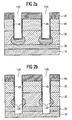
- Fig. 1 is a schematic diagram of a semiconductor device embodying the present invention.
- 10 designates an n + substrate, 20 a p + epitaxial layer (body lead), 30 a p epitaxial layer (body), 40 an n epitaxial layer (drain), 50 a drain, 60 an isolation region, 70 a Drain contact, 80 a first isolation layer, 90 a gate, 100 a gate oxide, 110 a second isolation layer, 120 a silicide region, 130 a source region and 140 a trench.
- This embodiment is a power-down power transistor having a n + -line type substrate.
- a first, second and third Epitaxiechicht 20, 30, 40 substrate 10 are provided on the n +, namely the first layer 20 of the p + conduction type on the substrate 10 as body connection region, the second layer 30 of p-conductivity type first on the Layer 20 as a body region and the third layer 40 of the n-type conductivity n on the second layer 30 as a drain region.
- the trench 140 which extends down to the substrate 10, includes a gate structure 90, 100 having a gate 90 and a gate oxide 100, the gate 100 being isolated from its surroundings by the isolation layers 90 and 110 and the isolation region 60.
- the source region 130 of the n + -line type is an implantation region.
- the source region 130 is characterized by a conductive layer 120 provided in the lower trench region in the form of a silicide layer is short-circuited with the first layer 20 and the substrate 10.
- Fig. 1 two such transistors are shown, wherein the right-hand transistor has a gate 90 connected to the right or connected to the outside and the left transistor has a gate 90 connected or interconnected to the rear (third dimension) by a transverse trench (not shown) ,
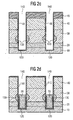
- FIGS. 2 a - f are schematic illustrations of the essential method steps for producing the semiconductor component according to FIG. 1.
- the n.sup. + Substrate 10 is provided and then the first p + type first layer 20 is epitaxially formed on the substrate 10, the second conductivity type second layer 30 on the first layer 20, and the third conductivity type third layer 40 n on the second layer 30.
- An oxide 45 is deposited thereon and a trench 140, which extends down to the second layer 20, is formed. The latter is done by forming a photomask on the oxide 45 and an anisotropic etching of the oxide 45 (hardmask) and the trench. Subsequently, a stray oxide 48 is formed in the trench 140. Thereafter, the implantation and diffusion of the source region 130 of the conduction type n + is performed in the lower part of the second layer 30 in the periphery of the trench 140.
- the trench 140 is then deepened down to the substrate 10, as illustrated in FIG. 2b.
- shorting of the source region 130 is accomplished by forming the conductive layer 120 in the lower trench region with the first layer 20 and the substrate 10.
- a metal e.g. Tungsten
- Subsequent etching removes the residual oxide metal.
- the deposition of oxide 110, the application of an auxiliary layer 55 and the etching back of the auxiliary layer 55 are then carried out.
- the oxide 110 is etched in the region above the remaining auxiliary layer 55 and a gate oxide 100 is formed. Then, the auxiliary layer 55 is removed and gate polysilicon is deposited over the resulting structure. The gate polysilicon is optionally doped and then etched back.
- a thicker oxide 80 is formed analogously to the oxide 110 in the upper region of the trench thermally or by deposition.
- anisotropic etching of the oxide 80 is then carried out in order to remove it from the top side of the gate polysilicon 90 and then a new deposition, doping and etching back of further gate polysilicon 90.
- Silicate glass (BPSG) is finally the isolation region 60 formed on the top of the trench.
- Contact holes for the drain connection are formed by means of a mask and the drain contact 70 is self-aligning implanted. Finally, the formation of the metal level takes place for the drain 50 to complete the transistor.
- the body is not realized by an epitaxial layer but by a p-implantation in the trench bottom and an outdiffusion before the source implantation.
- the present invention is not limited to the described transistor but may be applied to any more complicated structure, e.g. a thyristor structure can be applied.
- the body connection area is not absolutely necessary, but it is also possible to connect the body area directly.
Landscapes
- Insulated Gate Type Field-Effect Transistor (AREA)
- Electrodes Of Semiconductors (AREA)
- Metal-Oxide And Bipolar Metal-Oxide Semiconductor Integrated Circuits (AREA)
Claims (13)
- Composant semi-conducteur comprenant :un substrat (10) d'une première nature de conductivité (n+) ;une deuxième couche (30) de nature de conductivité (p), prévue au-dessus du substrat (10), comme région de body ;une troisième couche (40) de la première nature de conductivité (n), prévue sur la deuxième couche (30), comme région de drain ;une tranchée (140) qui arrive jusqu'au substrat (10) ;une structure de grille (90, 100) prévue dans la tranchée (140) ; etune région de source (130) de la première nature de conductivité (n+), prévue dans la deuxième couche (30) dans la périphérie de la tranchée (140) ;la région de source (130) étant court-circuitée avec la deuxième couche (30) et le substrat (10) par une couche (120) conductrice prévue dans la région inférieure de la tranchée.
- Composant semi-conducteur selon la revendication 1,
caractérisé en ce que sur le substrat (10), une première couche (20) de la deuxième nature de conductivité (p+) est prévue comme région de connexion de body sur laquelle la deuxième couche est prévue. - Composant semi-conducteur selon la revendication 2,
caractérisé en ce qu'au moins une de la première, deuxième et troisième couche (20, 30, 40) est une couche épitaxiale. - Composant semi-conducteur selon l'une quelconque des revendications précédentes,
caractérisé en ce que la région de source (130) est une région d'implantation. - Composant semi-conducteur selon l'une quelconque des revendications précédentes,
caractérisé en ce que la couche conductrice (120) est une couche silicide. - Composant semi-conducteur selon l'une quelconque des revendications précédentes,
caractérisé en ce que la première nature de conductivité est de type n. - Procédé pour la fabrication d'un composant semi-conducteur comprenant les étapes :mise à disposition d'un substrat (10) d'une première nature de conductivité (n+) ;prévision d'une deuxième couche (30) de la deuxième nature de conductivité (p) au dessus du substrat (10) ;prévision d'une troisième couche (40) de la première nature de conductivité (n) sur la deuxième couche (30) ;formation d'une tranchée (140) qui arrive jusqu'à la deuxième couche (20);formation d'une région de source (130) de la première nature de conductivité (n+) dans la partie inférieure de la deuxième couche (30) dans la périphérie de la tranchée (140) ;approfondissement de la tranchée (140) jusqu'au substrat (10) ;mise en court-circuit de la région de source (130) avec la deuxième couche (30) et le substrat (10) par la formation d'une couche (120) conductrice dans la région inférieure de la tranchée ; etformation d'une structure de grille (90, 100) dans la tranchée (140).
- Procédé selon la revendication 8,
caractérisé en ce qu'on prévoit, sur le substrat (10), une première couche (20) de la deuxième nature conductrice (p+) sur laquelle la deuxième couche est prévue. - Procédé selon la revendication 8,
caractérisé en ce qu'au moins une de la première, deuxième et troisième couche (20, 30, 40) est déposée de façon épitaxiale. - Procédé selon l'une quelconque des revendications précédentes 7 à 9,
caractérisé par en ce que la région de source (130) est implantée. - Procédé selon l'une quelconque des revendications précédentes 7 à 10,
caractérisé en ce que la couche conductrice (120) est une couche silicide qui est réalisée par déposition d'un métal, de préférence du tungstène, dans la tranchée (140) et par une silicidation thermique. - Procédé selon l'une quelconque des revendications précédentes 7 à 11,
caractérisé en ce que la première nature de conductivité est de type n. - Procédé selon l'une quelconque des revendications précédentes 7 à 11,
caractérisé en ce que la deuxième couche (30) est formée par une implantation dans le fond de la tranchée et une diffusion avant l'implantation de la source.
Applications Claiming Priority (2)
| Application Number | Priority Date | Filing Date | Title |
|---|---|---|---|
| DE10004984A DE10004984A1 (de) | 2000-02-04 | 2000-02-04 | Vertikales Halbleiterbauelement mit Source-Down-Design und entsprechendes Herstellungsverfahren |
| DE10004984 | 2000-02-04 |
Publications (3)
| Publication Number | Publication Date |
|---|---|
| EP1122796A2 EP1122796A2 (fr) | 2001-08-08 |
| EP1122796A3 EP1122796A3 (fr) | 2002-03-20 |
| EP1122796B1 true EP1122796B1 (fr) | 2006-04-05 |
Family
ID=7629859
Family Applications (1)
| Application Number | Title | Priority Date | Filing Date |
|---|---|---|---|
| EP01102123A Expired - Lifetime EP1122796B1 (fr) | 2000-02-04 | 2001-01-31 | Dispositif semi-conducteur vertical comportant une connexion source-substrat et procédé de fabrication correspondant |
Country Status (3)
| Country | Link |
|---|---|
| US (1) | US6576953B2 (fr) |
| EP (1) | EP1122796B1 (fr) |
| DE (2) | DE10004984A1 (fr) |
Families Citing this family (10)
| Publication number | Priority date | Publication date | Assignee | Title |
|---|---|---|---|---|
| JP4932088B2 (ja) | 2001-02-19 | 2012-05-16 | ルネサスエレクトロニクス株式会社 | 絶縁ゲート型半導体装置の製造方法 |
| GB0129450D0 (en) * | 2001-12-08 | 2002-01-30 | Koninkl Philips Electronics Nv | Trenched semiconductor devices and their manufacture |
| DE10239310B4 (de) * | 2002-08-27 | 2005-11-03 | Infineon Technologies Ag | Verfahren zur Herstellung einer elektrisch leitenden Verbindung zwischen einer ersten und einer zweiten vergrabenen Halbleiterschicht |
| US6790713B1 (en) * | 2002-09-09 | 2004-09-14 | T-Ram, Inc. | Method for making an inlayed thyristor-based device |
| US6605838B1 (en) * | 2002-09-30 | 2003-08-12 | International Business Machines Corporation | Process flow for thick isolation collar with reduced length |
| KR100574317B1 (ko) * | 2004-02-19 | 2006-04-26 | 삼성전자주식회사 | 게이트 구조물, 이를 갖는 반도체 장치 및 그 형성 방법 |
| US7456470B2 (en) * | 2004-10-01 | 2008-11-25 | International Rectifier Corporation | Top drain fet with integrated body short |
| US20090053869A1 (en) * | 2007-08-22 | 2009-02-26 | Infineon Technologies Austria Ag | Method for producing an integrated circuit including a trench transistor and integrated circuit |
| US8471331B2 (en) | 2011-08-15 | 2013-06-25 | Semiconductor Components Industries, Llc | Method of making an insulated gate semiconductor device with source-substrate connection and structure |
| KR102232766B1 (ko) * | 2015-01-05 | 2021-03-26 | 삼성전자주식회사 | 반도체 소자 및 이의 제조방법 |
Family Cites Families (6)
| Publication number | Priority date | Publication date | Assignee | Title |
|---|---|---|---|---|
| US5023196A (en) | 1990-01-29 | 1991-06-11 | Motorola Inc. | Method for forming a MOSFET with substrate source contact |
| JP3415326B2 (ja) * | 1995-04-28 | 2003-06-09 | 株式会社デンソー | 車両用発電機の出力制御装置 |
| DE19638439C2 (de) * | 1996-09-19 | 2000-06-15 | Siemens Ag | Durch Feldeffekt steuerbares, vertikales Halbleiterbauelement und Herstellungsverfahren |
| DE19638438A1 (de) * | 1996-09-19 | 1998-04-02 | Siemens Ag | Durch Feldeffekt steuerbares, vertikales Halbleiterbauelement |
| US6124612A (en) * | 1998-01-15 | 2000-09-26 | Siemens Aktiengesellschaft | FET with source-substrate connection and method for producing the FET |
| DE19801313C2 (de) | 1998-01-15 | 2001-01-18 | Siemens Ag | FET mit Source-Substratanschluß |
-
2000
- 2000-02-04 DE DE10004984A patent/DE10004984A1/de not_active Withdrawn
-
2001
- 2001-01-23 US US09/768,015 patent/US6576953B2/en not_active Expired - Lifetime
- 2001-01-31 DE DE50109408T patent/DE50109408D1/de not_active Expired - Lifetime
- 2001-01-31 EP EP01102123A patent/EP1122796B1/fr not_active Expired - Lifetime
Also Published As
| Publication number | Publication date |
|---|---|
| US20020135008A1 (en) | 2002-09-26 |
| US6576953B2 (en) | 2003-06-10 |
| EP1122796A2 (fr) | 2001-08-08 |
| DE10004984A1 (de) | 2001-08-16 |
| DE50109408D1 (de) | 2006-05-18 |
| EP1122796A3 (fr) | 2002-03-20 |
Similar Documents
| Publication | Publication Date | Title |
|---|---|---|
| DE68918619T2 (de) | Verfahren zum Herstellen eines selbstisolierenden source/drain-Kontaktes in einem MOS-Transistor. | |
| DE19845003C1 (de) | Vertikaler Feldeffekttransistor mit innenliegendem ringförmigen Gate und Herstellverfahren | |
| DE4011276C2 (de) | Feldeffekttransistor mit isoliertem Gate (IGFET) und Verfahren zu seiner Herstellung | |
| DE69124646T2 (de) | MOS-Halbleiterbauelement und dessen Herstellungsverfahren | |
| DE102007063728B4 (de) | Halbleiterbauelementanordnung mit einem Trench-Transistor | |
| DE69634764T2 (de) | Halbleiteranordnung und Verfahren zu ihrer Herstellung | |
| DE102004055640B4 (de) | LDMOS-Transistorvorrichtung, Integrierter Schaltkreis und Herstellungsverfahren hiervon | |
| DE4445345C2 (de) | Verfahren zur Herstellung eines Bipolartransistors | |
| DE3686490T2 (de) | Halbleiterstruktur. | |
| DE69214339T2 (de) | Struktur und Verfahren für die Bildung selbstjustierender Kontakte | |
| DE102021134457A1 (de) | Verfahren und strukturen zum kontaktieren des abschirmleiters in einer halbleitervorrichtung | |
| EP1122796B1 (fr) | Dispositif semi-conducteur vertical comportant une connexion source-substrat et procédé de fabrication correspondant | |
| EP0764982B1 (fr) | Procédé pour la fabrication d'un circuit CMOS intégré | |
| DE3931127C2 (de) | Verfahren zum Herstellen einer Halbleitereinrichtung | |
| DE10224201A1 (de) | Halbleiterbauelement mit Durchbruchstrompfad | |
| EP0687013A1 (fr) | Transistor bipolaire et procédé de fabrication | |
| DE4130890A1 (de) | Verfahren zur herstellung eines kondensators unter verwendung des feldeffekttransistor-prozesses und mit hilfe des verfahrens hergestellte struktur | |
| DE10063443B4 (de) | Verfahren zur Herstellung einer Elektrode eines mittels Feldeffekt steuerbaren Halbleiterbauelements und mittels Feldeffekt steuerbares Halbleiterbauelement | |
| DE4122712A1 (de) | Halbleitervorrichtung | |
| DE102006029701B4 (de) | Halbleiterbauteil sowie Verfahren zur Herstellung eines Halbleiterbauteils | |
| EP0716453B1 (fr) | MOSFET sur substrat du type SOI | |
| DE102006001922B3 (de) | Lateraler Leistungstransistor und Verfahren zu dessen Herstellung | |
| DE3854005T2 (de) | Speicherzelle. | |
| EP0651433B1 (fr) | Procédé de fabrication d'un trou de contact sur une région dopée | |
| DE69826551T2 (de) | Vertikaler Feldeffekttransistor mit isolierter Steuerelektrode, Verfahren zu dessen Herstellung und entsprechende integrierte Schaltung |
Legal Events
| Date | Code | Title | Description |
|---|---|---|---|
| PUAI | Public reference made under article 153(3) epc to a published international application that has entered the european phase |
Free format text: ORIGINAL CODE: 0009012 |
|
| AK | Designated contracting states |
Kind code of ref document: A2 Designated state(s): AT BE CH CY DE DK ES FI FR GB GR IE IT LI LU MC NL PT SE TR Kind code of ref document: A2 Designated state(s): DE FR IT |
|
| AX | Request for extension of the european patent |
Free format text: AL;LT;LV;MK;RO;SI |
|
| PUAL | Search report despatched |
Free format text: ORIGINAL CODE: 0009013 |
|
| AK | Designated contracting states |
Kind code of ref document: A3 Designated state(s): AT BE CH CY DE DK ES FI FR GB GR IE IT LI LU MC NL PT SE TR |
|
| AX | Request for extension of the european patent |
Free format text: AL;LT;LV;MK;RO;SI |
|
| 17P | Request for examination filed |
Effective date: 20020918 |
|
| AKX | Designation fees paid |
Free format text: DE FR IT |
|
| 17Q | First examination report despatched |
Effective date: 20050426 |
|
| GRAP | Despatch of communication of intention to grant a patent |
Free format text: ORIGINAL CODE: EPIDOSNIGR1 |
|
| GRAS | Grant fee paid |
Free format text: ORIGINAL CODE: EPIDOSNIGR3 |
|
| GRAA | (expected) grant |
Free format text: ORIGINAL CODE: 0009210 |
|
| AK | Designated contracting states |
Kind code of ref document: B1 Designated state(s): DE FR IT |
|
| PG25 | Lapsed in a contracting state [announced via postgrant information from national office to epo] |
Ref country code: IT Free format text: LAPSE BECAUSE OF FAILURE TO SUBMIT A TRANSLATION OF THE DESCRIPTION OR TO PAY THE FEE WITHIN THE PRESCRIBED TIME-LIMIT;WARNING: LAPSES OF ITALIAN PATENTS WITH EFFECTIVE DATE BEFORE 2007 MAY HAVE OCCURRED AT ANY TIME BEFORE 2007. THE CORRECT EFFECTIVE DATE MAY BE DIFFERENT FROM THE ONE RECORDED. Effective date: 20060405 |
|
| REF | Corresponds to: |
Ref document number: 50109408 Country of ref document: DE Date of ref document: 20060518 Kind code of ref document: P |
|
| PLBE | No opposition filed within time limit |
Free format text: ORIGINAL CODE: 0009261 |
|
| STAA | Information on the status of an ep patent application or granted ep patent |
Free format text: STATUS: NO OPPOSITION FILED WITHIN TIME LIMIT |
|
| 26N | No opposition filed |
Effective date: 20070108 |
|
| EN | Fr: translation not filed | ||
| PG25 | Lapsed in a contracting state [announced via postgrant information from national office to epo] |
Ref country code: FR Free format text: LAPSE BECAUSE OF FAILURE TO SUBMIT A TRANSLATION OF THE DESCRIPTION OR TO PAY THE FEE WITHIN THE PRESCRIBED TIME-LIMIT Effective date: 20070309 |
|
| PG25 | Lapsed in a contracting state [announced via postgrant information from national office to epo] |
Ref country code: FR Free format text: LAPSE BECAUSE OF FAILURE TO SUBMIT A TRANSLATION OF THE DESCRIPTION OR TO PAY THE FEE WITHIN THE PRESCRIBED TIME-LIMIT Effective date: 20060405 |
|
| PGFP | Annual fee paid to national office [announced via postgrant information from national office to epo] |
Ref country code: DE Payment date: 20170316 Year of fee payment: 17 |
|
| REG | Reference to a national code |
Ref country code: DE Ref legal event code: R119 Ref document number: 50109408 Country of ref document: DE |
|
| PG25 | Lapsed in a contracting state [announced via postgrant information from national office to epo] |
Ref country code: DE Free format text: LAPSE BECAUSE OF NON-PAYMENT OF DUE FEES Effective date: 20180801 |