EP1124182A2 - Übertragung von Ergebnissen in einem Prozessor, und Verfahren zur Kompilierung - Google Patents
Übertragung von Ergebnissen in einem Prozessor, und Verfahren zur Kompilierung Download PDFInfo
- Publication number
- EP1124182A2 EP1124182A2 EP01300947A EP01300947A EP1124182A2 EP 1124182 A2 EP1124182 A2 EP 1124182A2 EP 01300947 A EP01300947 A EP 01300947A EP 01300947 A EP01300947 A EP 01300947A EP 1124182 A2 EP1124182 A2 EP 1124182A2
- Authority
- EP
- European Patent Office
- Prior art keywords
- value
- instruction
- instructions
- register
- processor
- Prior art date
- Legal status (The legal status is an assumption and is not a legal conclusion. Google has not performed a legal analysis and makes no representation as to the accuracy of the status listed.)
- Withdrawn
Links
Images




Classifications
-
- G—PHYSICS
- G06—COMPUTING OR CALCULATING; COUNTING
- G06F—ELECTRIC DIGITAL DATA PROCESSING
- G06F8/00—Arrangements for software engineering
- G06F8/40—Transformation of program code
- G06F8/41—Compilation
- G06F8/44—Encoding
- G06F8/441—Register allocation; Assignment of physical memory space to logical memory space
-
- G—PHYSICS
- G06—COMPUTING OR CALCULATING; COUNTING
- G06F—ELECTRIC DIGITAL DATA PROCESSING
- G06F8/00—Arrangements for software engineering
- G06F8/40—Transformation of program code
- G06F8/41—Compilation
- G06F8/44—Encoding
- G06F8/445—Exploiting fine grain parallelism, i.e. parallelism at instruction level
- G06F8/4452—Software pipelining
-
- G—PHYSICS
- G06—COMPUTING OR CALCULATING; COUNTING
- G06F—ELECTRIC DIGITAL DATA PROCESSING
- G06F9/00—Arrangements for program control, e.g. control units
- G06F9/06—Arrangements for program control, e.g. control units using stored programs, i.e. using an internal store of processing equipment to receive or retain programs
- G06F9/30—Arrangements for executing machine instructions, e.g. instruction decode
- G06F9/38—Concurrent instruction execution, e.g. pipeline or look ahead
- G06F9/3824—Operand accessing
- G06F9/383—Operand prefetching
- G06F9/3832—Value prediction for operands; operand history buffers
-
- G—PHYSICS
- G06—COMPUTING OR CALCULATING; COUNTING
- G06F—ELECTRIC DIGITAL DATA PROCESSING
- G06F9/00—Arrangements for program control, e.g. control units
- G06F9/06—Arrangements for program control, e.g. control units using stored programs, i.e. using an internal store of processing equipment to receive or retain programs
- G06F9/30—Arrangements for executing machine instructions, e.g. instruction decode
- G06F9/38—Concurrent instruction execution, e.g. pipeline or look ahead
- G06F9/3836—Instruction issuing, e.g. dynamic instruction scheduling or out of order instruction execution
-
- G—PHYSICS
- G06—COMPUTING OR CALCULATING; COUNTING
- G06F—ELECTRIC DIGITAL DATA PROCESSING
- G06F9/00—Arrangements for program control, e.g. control units
- G06F9/06—Arrangements for program control, e.g. control units using stored programs, i.e. using an internal store of processing equipment to receive or retain programs
- G06F9/30—Arrangements for executing machine instructions, e.g. instruction decode
- G06F9/38—Concurrent instruction execution, e.g. pipeline or look ahead
- G06F9/3836—Instruction issuing, e.g. dynamic instruction scheduling or out of order instruction execution
- G06F9/3838—Dependency mechanisms, e.g. register scoreboarding
- G06F9/384—Register renaming
Definitions
- the present invention relates to communicating instruction results in processors and to compiling methods for processors.
- the present invention relates to allocating registers for storing instruction results in processors such as microprocessors.
- a high rate of instruction execution is usually required of the target machine (e.g. microprocessor). Execution time is often dominated by loop structures within the application program.
- a processor may include a plurality of individual execution units, with each individual unit being capable of executing one or more instructions in parallel with the execution of instructions by the other execution units.
- Such a plurality of execution units can be used to provide a so-called software pipeline made up of a plurality of individual stages.
- Each software pipeline stage has no fixed physical correspondence to particular execution units. Rather, when a loop structure in an application program is compiled the machine instructions which make up an individual iteration of the loop are scheduled for execution by the different execution units in accordance with a software pipeline schedule. This schedule is divided up into successive stages and the instructions are scheduled in such a way as to permit a plurality of iterations to be carried out in overlapping manner by the different execution units with a selected loop initiation interval between the initiations of successive iterations.
- loop-variant values i.e. expressions which must be reevaluated in each different iteration of the loop, that must be communicated between different instructions in the pipeline.
- loop-variant values it is possible to store them in a so-called rotating register file.
- each loop-variant value is assigned a logical register number within the rotating register file, and this logical register number does not change from one iteration to the next.
- Inside the rotating register file each logical register number is mapped to a physical register within the register file and this mapping is rotated each time a new iteration is begun, i.e. each time a pipeline boundary is closed.
- corresponding instructions in different iterations can all refer to the same logical register number, making the compiled instructions simple, whilst avoiding a value produced by one iteration from being overwritten by a subsequently-executed instruction of a different iteration.
- a processor including: instruction issuing means for issuing, in a predetermined sequence, instructions to be executed, the said sequence of instructions including preselected value-producing instructions which, when executed, produce respective values; instruction executing means for executing the issued instructions; register means, having a plurality of registers, for storing values produced by the executed instructions; sequence number assigning means for assigning said values produced by said value-producing instructions respective sequence numbers according to the order of issuance of their respective value-producing instructions; and register allocating means for allocating each said produced value one of the said registers, for storing that produced value, in dependence upon the sequence number assigned to that value.
- the compiler task in allocating registers is simplified.
- the register means may be in the form of a rotating register file and the registers may be remapped (renamed) each time one of the preselected value-producing instructions is issued.
- the instruction set for such a processor can also be more compact in that value-producing instructions need not specify any destination register for storing their respective produced values.
- a compilation method for converting a sequence of high-level program instructions into a corresponding sequence of low-level instructions to be executed by a processor, the method comprising the steps of: determining which said low-level instructions of the said corresponding sequence are preselected value-producing instructions and which are preselected value-requiring instructions, each said value-producing instruction being an instruction which when executed will produce a value, and each said value-requiring instruction being an instruction which when executed will require the said value produced by a previously-issued value-producing instruction; assigning said produced values respective sequence numbers according to the order in which their respective value-producing instructions will be issued during execution; and coding each said value-requiring instruction with information for use by the said processor during execution to identify the said produced value required by that instruction, that information being dependent on the said sequence number assigned to that produced value.
- a computer program which, when run on a computer, causes the computer to carry out a compilation method embodying the aforesaid second aspect of the present invention.
- a computer program which, when run on a computer, causes the computer to carry out a compilation method for converting a sequence of high-level program instructions into a corresponding sequence of low-level instructions to be executed by a processor
- the computer program including: a determining portion for determining which said low-level instructions of the said corresponding sequence are preselected value-producing instructions and which are preselected value-requiring instructions, each said value-producing instruction being an instruction which when executed will produce a value and each said value-requiring instruction being an instruction which when executed will require the value produced by a previously-issued value-producing instruction; an assigning portion for assigning the produced values respective sequence numbers according to the order in which their respective value-producing instructions will be issued during execution; and a coding portion for coding each value-requiring instruction with information for use by the processor to identify the said produced value required by that instruction, that information being dependent on the sequence number assigned to that produced value.
- Fig. 1 shows parts of a processor embodying the present invention.
- the processor is a very long instruction word (VLIW) processor with hardware support for software pipelining and cyclic register renaming.
- the processor 1 includes an instruction issuing unit 10, a schedule storage unit 12, respective first, second and third execution units 14, 16 and 18, and a register file 20.
- the instruction issuing unit 10 has three issues slots IS1, IS2 and IS3 connected respectively to the first, second and third execution units 14, 16 and 18.
- a first bus 22 connects all three execution units 14, 16 and 18 to the register file 20.
- a second bus 24 connects the first and second units 14 and 16 (but not the third execution unit 18 in this embodiment) to a memory 26 which, in this example, is an external random access memory (RAM) device.
- the memory 26 could alternatively be a RAM internal to the processor 1.
- FIG. 1 shows shared buses 22 and 24 connecting the execution units to the register file 20 and memory 26, it will be appreciated that alternatively each execution unit could have its own independent connection to the register file and memory.
- the processor 1 performs a series of processing cycles.
- the instruction issuing unit 10 can issue one instruction at each of the issue slots IS1 to IS3.
- the instructions are issued according to a software pipeline schedule (described below) stored in the schedule storage unit 12.
- the instructions issued by the instructing issuing unit 10 at the different issue slots are executed by the corresponding execution units 14, 16 and 18.
- each of the execution units can execute more than one instruction at the same time, so that execution of a new instruction can be initiated prior to completion of execution of a previous instruction issued to the execution unit concerned.
- each execution unit 14, 16 and 18 has access to the register file 20 via the first bus 22. Values held in registers contained in the register file 20 can therefore be read and written by the execution units 14, 16 and 18. Also, the first and second execution units 14 and 16 have access via the second bus 24 to the external memory 26 so as to enable values stored in memory locations of the external memory 26 to be read and written as well.
- the third execution unit 18 does not have access to the external memory 26 and so can only manipulate values contained in the register file 20 in this embodiment.
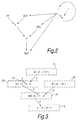
- the process of compiling this loop for the Fig. 1 processor begins with the creation of a symbolic data-flow graph as shown in Fig. 2.
- the next step is to perform a variety of optimisations to convert the Fig. 2 data-flow graph into a form which is closer to actual machine instructions of the Fig. 1 processor.
- the compiler determines what values change within the loop (loop-variant values) and what values remain the same (loop-invariant values). For example, the value of da is not altered at all during the loop.
- each array dx and dy will be stored in memory locations in the external memory 26 (Fig. 1) and so references to them in the Fig. 2 data-flow graph must be converted into corresponding memory access operations.
- each array dx and dy needs at least one pointer for pointing to the storage locations in the external memory 26 where the elements of the array are stored.
- Each such pointer is held in a register of the register file 20.
- the constant value da could be dealt with using a similar pointer to its location in the memory, as the value is loop-invariant it is more convenient and fast to keep it directly in its own register of the register file 20 during execution of the loop.
- the compiler takes account of any advantageous features of the available processor instructions such as auto-increment addressing modes.
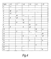
- FIG. 3 shows the individual machine instructions and their dependence relationships (an arrow pointing from a first instruction to a second instruction indicates that the second instruction is dependent upon the result of execution of the first instruction).
- Each arrow in Fig. 3 also has associated with it a number which denotes the number of processor cycles required to complete the execution of the instruction from which the arrow points.
- the first instruction I1 is Fig. 3 is a load instruction "ld v0, (r1++)". This instruction is used to load into a register v0 of the register file 20 the value of the array element dx(i). The value is read from the memory location in the external memory 26 pointed to by a further register r1 of the register file.
- the "++" after "r1" in instruction I1 denotes that after reading the memory location pointed to by the register r1, the register r1 is to be incremented to point to the next successive location in the external memory 26.
- This is an example of the compiler taking advantage of an auto-increment addressing mode feature of the processor 1.
- the second instruction I2 is a multiply instruction "mul v1, r3, v0". This multiply instruction is used to multiply the value of dx(i), loaded in the first instruction I1 into the register v0, by the value of da held in another register r3 of the register file 20. The result of the multiplication is stored in a register v1 of the register file 20.
- the third instruction 13 in Fig. 3 is another load instruction "ld v2, (r2++)".
- This second load instruction is used to load into a register v2 of the register file 20 the value of the array element dy(i) held in the memory location pointed to by a register r2 of the register file 20.
- This second load instruction is also an auto-increment addressing mode instruction which increments the register r2 automatically after the read operation so that it then points to the next memory location after the location just read.
- the fourth instruction 14 in Fig. 3 is an add instruction "add v3, v1, v2". This instruction adds together the respective values held in the registers v1 and v2 (i.e. da*dx(i) and dy(i)) and stores the result in a further register v3 of the register file 20.
- the fifth instruction I5 in Fig. 3 is a store instruction "st v3, (r4++)". This instruction is used to store the value held in the register v3 in the external memory 26 at the memory location for dy(i) pointed to by a further register r4 contained in the register file 20.
- the memory location (pointed to by the register r2) from which dy(i) is read in the second load instruction I3 must be the same memory location (pointed to by the register r4) into which dy(i) is written in the store instruction I5. It might therefore be considered better to use a single register (e.g. r2) to point to dy(i) in both the second load instruction 13 and the store instruction I5. However, in this example the use of a single register is not possible because (as will be apparent from the later description) the software pipelining results in the second load instruction I3 in the next iteration being executed before the store instruction I5 in the current iteration.
- the register r2 would have been incremented by the load instruction I3 of the next iteration before it could be used by the store instruction I5 of the current iteration. For this reason, the two registers r2 and r4 are used in Fig. 3 to point to dy(i), the two registers having the same value at the start of each iteration and each being incremented once during the course of the iteration but the incrementing of r4 being deferred relative to that of the register r2.
- Fig. 3 it can be seen that the results produced by the instructions I1 to I4 are all loop-variant values which must be distinguished from one another in different iterations. For this reason, these intermediate values are assigned temporary register identifiers (numbers) v0 to v3. These are not the final register assignments but are merely temporary labels for the instruction results (arrows in the data-flow graph) applied by the compiler.
- the registers r1 to r4 are assigned final (permanent) register numbers because the computation results destined for registers r1 to r4 have latencies and lifetimes that do not span more than one iteration, i.e. by the time r1 needs to be rewritten in a given iteration, the produced value stored in r1 in a previous iteration is no longer needed by any other iteration.
- the process of executing one iteration of the loop as shown in Fig. 3 involves evaluating the nodes in the tree starting at the nodes with no predecessor and working towards the root of the tree. In this case, therefore, the order of execution is from I1 to I5 in Fig. 3.
- the next stage of the compiling process is to create a software pipeline schedule.
- the first phase of software pipelining involves determining a loop initiation interval (II), i.e. the interval between initiation of successive iterations of the loop.
- II loop initiation interval
- This loop initiation interval depends on the available resources in the processor in comparison with the number of instructions to execute, as well as the presence of any cycles in the data-flow graph.
- the Fig. 1 processor has three instruction issue slots IS1 to IS3 and three execution units 14, 16 and 18, of which only the first and second execution units 14 and 16 are capable of accessing the external memory 26.
- the execution units may be "specialised" units in the sense that they are optimised individually for carrying out different tasks. For example, it may be that only certain of the execution units are capable of performing certain types of instruction.
- the loop initiation interval II is determined as two processor cycles. Also, it will be assumed that only the third execution unit 18 is equipped with the resources (e.g. an arithmetic and logic unit ALU) necessary to execute add and multiple instructions.
- the resources e.g. an arithmetic and logic unit ALU
- the next phase is to create a schedule which obeys a so-called modulo scheduling constraint.
- This constraint relates to the instructions making up one iteration (i.e. the instructions I1 to I5 in Fig. 3).
- an instruction may be scheduled for issue from the slot concerned at cycle x if and only if there are no instructions scheduled for issue from the same issue slot at cycle y, where y modulo II is equal to x.
- This modulo constraint if met, ensures that each issue slot only issues a maximum of one instruction per processor cycle.
- Table 1 below presents a modulo scheduling table corresponding to the Fig. 3 tree structure.
- Table 1 shows how the five instructions I1 to I5 making up one iteration of the loop are scheduled.
- columns 3 to 5 of the table show the cycle in the schedule when each instruction is issued, the software pipeline stage in which it occurs, and the issue slot by which the instruction is issued (i.e. the execution unit which executes the instruction).
- the final four columns indicate logical register numbers and shading is used to illustrate value lifetimes, as will be explained later in detail with reference to Figs. 5, 6(A) and 6(B).
- the schedule in Table 1 relates to one iteration only. Every II cycles another iteration is initiated according to the same schedule. Thus, when the current iteration is at stage 1, the immediately-preceding iteration will be at stage 2, the iteration before that will be at stage 3, the iteration before that at stage 4 and the iteration before that at stage 5.
- the instructions are scheduled for issue by the same issue slots in all iterations, that each issue slot issues the same instruction every II cycles.
- the notation is as follows:
- the first iteration commences with the issuance from issue slot 1 of the first load instruction L1. No instructions are initiated in cycle 1.
- the multiply instruction M of the first iteration is also issued from issue slot 3.
- cycle 3 only the second load instruction L2 of the first iteration is issued. It will be appreciated that, at the time of issuance of L2 of the first iteration, L1 of the second iteration is still not complete. It follows that the first execution unit 14 in the Fig. 1 processor must be capable of executing these two load instructions in parallel with one another in this embodiment.
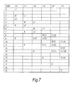
- the pipelined nature of the execution of the iteration can be seen from Fig. 4.
- v0 to "v3" are merely temporary identifiers (labels) assigned to the registers. These temporary register identifiers must be translated into logical register identifiers to be specified by the instructions. This translation task is performed by the compiler, taking into account the way in which registers are allocated by the processor at run-time.
- Fig. 5 shows a schematic representation of one part of a register file 120 in the previously-considered processor.
- the part 120R shown in Fig. 5 is the part used by the processor for holding loop-variant values.
- the register file 120 may also have another part (not shown in Fig. 5) for holding loop-invariant values.
- the part 120R comprises a plurality (in this example 16) of registers r0 to r15 arranged at successive addresses in the register file 20.
- the logical register identifier specified in an instruction is mapped to a physical register address using a mapping offset OFFSET.
- the mapping offset OFFSET is 10, which means that a logical register identifier s0 is mapped to physical register r10.
- Logical register identifier s1 is mapped to physical register r11, and so on.
- the mapping "wraps around" the part 120R so that, for example, logical register identifier s6 maps to physical register r0 when OFFSET equals 10.
- mapping offset value OFFSET is changed each time execution of a new iteration is commenced, i.e. every II processor cycles.
- Changing the mapping offset value has the effect of changing the mapping between the logical register identifiers specified in the instructions and the actual physical registers in the part 20R of the register file 20. This is equivalent to renaming the registers.
- the instructions which are executed in software pipelined manner need to keep the same logical register identifiers irrespective of the particular iteration being performed.
- the renaming of the registers must then be such as to provide each loop-variant value produced in any given iteration with its own register, accessible as necessary by any other instructions requiring that value, for as long as the value is needed (i.e. for the lifetime of the value, shown by shading in the relevant one of the four final columns in Table 1).
- the register for storing the value produced by the first load instruction issued in cycle 0 is assigned the temporary register identifier v0, and the produced value concerned has a minimum lifetime of three processor cycles because it is needed in cycle 2 as one of the input operands of the multiply instruction.
- the value produced by the multiply instruction issued in cycle 2 is assigned the temporary register identifier v1, and this produced value has a minimum lifetime of four processor cycles because it is needed by the add instruction in cycle 5.
- Figs. 6(A) and 6(B) the way in which, for the previously-considered processor, the temporary register identifiers v0 to v3 are translated by the compiler into the logical register identifiers s0 to s8 as shown in Table 1 will be explained.
- the mapping offset value OFFSET is 10.
- the first load instruction needs to be allocated a physical register in which to store the loaded value.
- this value is the first value requiring a register, that register is specified using the logical register identifier s0 which is mapped within the register file 120 to the physical register r10.
- the multiply instruction requires the value produced by the first load instruction of the first iteration. Because of the renaming of the registers that took place at the start of cycle 2, the logical register identifier sl must be used to retrieve that value from physical register r10. The logical register identifier in the first load instruction of the second iteration must be the same (s0) as that in the first load instruction of the first iteration. The multiply instruction in the first iteration must also be provided with a register for storing its result. The first free register, after the registers r9 and r10 currently in use, is the register r11, corresponding to logical register identifier s2.
- the second load instruction of the first iteration is issued.
- This instruction requires a register in which to store its loaded value.
- the first free register after the registers r9 to r11 already in use, is the register r12.
- r12 must be reserved by the compiler for the produced value of a subsequent iteration, so the loaded value produced by the second load instruction of the first iteration is allocated the register r13, requiring the logical register identifier s4.
- cycle 4 the multiply instruction of the second iteration and the first load instruction of the third iteration are issued.
- the logical register identifiers for these instructions are the same as for the previous multiply and first load instructions.
- the physical register r10 can be reused for storing the result of the multiply instruction of the second iteration, as the lifetime of the loop-variant value stored in that register in the previous iteration expired in cycle 2.
- the issued instructions are the add instruction of the first iteration and the second load instruction of the second iteration.
- the input operands for the add instruction are contained in the registers r11 and r13, requiring the add instruction to specify as logical register identifiers s3 and s5.
- the register r14 which is the first free register after the in-use register r13, is allocated for the storage of the result of the add instruction. This register is specified by the logical register identifier s6.
- the reason why the register r12 had to be skipped in the first iteration can now be seen.
- the logical register identifier s4 used to allocate a register for storing the result of the second load instruction of the second iteration must be the same as the logical register identifier specified in the corresponding second load instruction of the first iteration. Had s4 been mapped to r12 in the first iteration, s4 would map to r11 in the second iteration. However, this cannot be done because r11, which is the register storing the value produced by the multiply instruction of the first iteration, is still in use at the beginning of cycle 5.
- Table 2 presents a modulo scheduling table corresponding to Table 1 but in accordance with an embodiment of the present invention.
- Schedule time Instruction allocation to schedule Value sequence stage cycle issue slot 1 issue slot 2 issue slot 3 s1 s2 s3 1 0 1d (r1++) 0 0 1 1 2 2 3 2 2 mul @5, r3 4 4 5 3 1d (r2++) 6 6 7 3 4 8 8 9 5 add @5,@6 10 10 11 4 6 12 12 13 7 14 14 15 5 8 16 16 17 9 st @7, (r4++) 18 18 19
- Each value produced during the execution of a software pipelined loop schedule is assigned a sequence number by the compiler during compilation. For example, the first value produced has the sequence number 0, and subsequently-produced values are numbered in increasing sequential order.
- a loop schedule is software-pipelined there will be k iterations of the loop active concurrently, where k is the number of software pipeline stages after scheduling has taken place. The k iterations are executed in time-overlapping manner, with each successive iteration starting II cycles after the previous iteration.
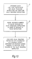
- Fig. 7 presents again the table of Fig. 4 described previously, but with numbers added in parentheses against certain instructions in order to illustrate how sequence numbers are assigned to values during compilation.
- This load instruction is a value-producing instruction as it produces the value dx(i) needed by the subsequent multiply instruction M of that iteration. It is assumed, as shown in Fig. 7, that the sequence number given by the compiler to the value produced by the cycle-8 first load instruction L1 is 0.
- another value-producing instruction is also issued by the instruction issuing unit 10 simultaneously with the first load instruction L1 of the fifth iteration. That other instruction is the multiply instruction M of the preceding (fourth) iteration. That simultaneously-issued value-producing instruction is issued from issue slot 3, which is after issue slot 1 in a predetermined order of the issue slots (1 ⁇ 2 ⁇ 3), and so the compiler allocates the value produced by the multiply instruction the next sequence number after the sequence number allocated to the value produced by the first load instruction L1, i.e. the sequence number 1.
- the compiler can systematically assign different sequence numbers to the values produced by those instructions.
- the assignment is made systematic (predictable) by assigning the sequence numbers in the predetermined order of the issue slots of the simultaneously-issued instructions.
- issue slot 1 issues another value-producing instruction, namely the second load instruction L2 of the fourth iteration.
- the value produced by this instruction is accordingly assigned sequence number 2.
- the add instruction A of the third iteration is issued from issue slot 3 in cycle 9.
- this instruction is a value-producing instruction and so the value produced by the instruction must be assigned a sequence number.
- the sequence number assigned to the value produced by the add instruction in cycle 9 is 3 because the issue slot (issue slot 3) for the add instruction concerned follows (in the predetermined order of issue slots) the issue slot (slot 1) from which the other simultaneously-issued value-producing instruction (L2 of the fourth iteration) was issued.
- the store instruction for the first iteration also issued in cycle 9, is not a value-producing instruction. In fact, it is a value-consuming instruction. Accordingly, no sequence number is assigned to any value associated with the store instruction.
- the processor allocates registers to the produced values in accordance with the order of issuance of the value-producing instructions which will produce those values, so that the produced values having the sequence numbers 0 to 5 in Fig. 7 are allocated to registers as shown in Fig. 8.
- This multiply instruction has a first operand specified as "@5" and a second operand specified as "r3".
- the second operand is straightforward, and simply denotes the content of register r3 as in Table 1.
- This register stores the loop-invariant value da.
- the reference "@5" for the first operand denotes that the value required for the first operand is the value having the sequence number 5 less than the present sequence number.
- the processor knows at execution time that it should use as the first operand the value whose assigned sequence number is 5 less than the current sequence number, namely the value produced by the first load instruction L1 issued in cycle 8. It also knows that the register allocated for storing the L1 result will be 5 registers in front of the latest-allocated register in the renameable part of the register file 20, i.e. the register having the logical register identifier 5.
- each input value needed by a value-requiring instruction such as the multiply instruction M can be specified precisely by the difference between the sequence number assigned to that input value and the sequence number reached at the point at which the value-requiring instruction is issued.
- This difference e.g. "@5"
- sequence offset may be referred to as a sequence offset.
- Fig. 9 shows in more detail parts of the Fig. 1 processor which, in one embodiment of the present invention, perform the functions of sequence number assignment for the produced values and register allocation and identification.
- the register file 20 has N registers in total, of which the lower-numbered K registers make up a statically-addressed region 20S and the higher-numbered N-K registers make up a dynamically-addressed (renameable) region 20R.
- This renameable region is generally similar to the part 120R already described with reference to Fig. 5.
- the registers of the statically-addressed region 20S are used for storing loop-invariant values, whilst the registers of the renameable region 20R are used for storing loop-variant values.
- a value-producing instruction detecting unit 30 is provided which detects when a value-producing instruction is issued.
- the value-producing instruction detecting unit 30 is conveniently included in the instruction issuing unit 10 of Fig. 1. Upon detecting the issuance of such an instruction, the value-producing instruction detecting unit 30 produces a RENAME signal.
- the RENAME signal is applied to a register renaming unit 32.
- the register renaming unit 32 is connected to a mapping offset storing unit 34 which stores a mapping offset value OFFSET.
- the register renaming unit 32 decrements by one the mapping offset value OFFSET stored in the mapping offset storing unit 34.
- the mapping offset value OFFSET stored in the mapping offset storing unit 34 is applied to a mapping unit 36.
- the mapping unit 36 also receives a logical register identifier (R) and outputs a physical register address (P).
- the logical register identifier (number) is an integer in the range from 0 to N-1.
- the mapping unit 36 implements a bijective mapping from logical register identifiers to physical register addresses. Each physical register address is also an integer in the range 0 to N-1 and identifies directly one of the actual hardware registers.
- the next free register in the renameable region 20R is allocated automatically to the value to be produced. That register is simply the register having the logical register number 0, i.e. the physical register number K+
- the execution unit which will execute the instruction is informed of the physical register number of the allocated register so that when the value is eventually produced it can be stored in the physical register concerned. Then the mapping offset value OFFSET is decremented by 1 in accordance with the RENAME signal issued by the detecting unit 30.
- the register storing the required value is specified in the instruction using its sequence offset relative to the latest-allocated register.
- This sequence offset can be used directly to provide the logical register identifier R.
- the sequence offset is therefore applied to the mapping unit 30 which then produces the corresponding physical register number P.
- the sequence offset "@5" provides the logical register identifier (5) of the required register directly.
- an issued instruction can be both a value-producing instruction and a value-requiring instruction.
- Fig. 10 parts of a compilation method for use in converting a sequence of high-level program instructions into a corresponding sequence of low-level instructions to be executed by the Fig. 1 processor will now be explained.
- the compilation method may include the steps described above with reference to Figs. 2, 3 and Table 1 for producing a software pipeline schedule.
- a first step S1 in Fig. 10 the compiler determines which low-level instructions of the corresponding sequence are preselected value-producing instructions and which low-level instructions of the corresponding sequence are preselected value-requiring instructions.
- the instructions I1 to I4 in Fig. 3 are all preselected value-producing instructions.
- the instructions 12, I4 and 15 are all preselected value-requiring instructions which require the produced values of previously-issued value-producing instructions.
- step S2 the compiler assigns sequence numbers to the produced values of the value-producing instructions in the order of issuance of those instructions.
- the assigned sequence numbers must reflect all overlapping iterations in the case of a software pipeline loop, as described previously with reference to Fig. 7.
- each value-requiring instruction is coded with information, such as the above-mentioned sequence offset, dependent on the sequence number assigned to the produced value that is required by the value-requiring instruction concerned.
- a compilation method embodying the present invention can be implemented by a general-purpose computer operating in accordance with a computer program.
- This computer program may be carried by any suitable carrier medium such as a storage medium (e.g. floppy disc or CD Rom) or a signal.
- a carrier signal could be a signal downloaded via a communications network such as the Internet.
- the appended computer program claims are to be interpreted as covering a computer program by itself or in any of the above-mentioned forms.
- sequence offset is simply the difference between the sequence number assigned to the input value concerned and the assigned sequence number reached when the instruction is issued. This makes the compiler task in terms of register allocation in the rotating (renameable) part of the register file much more simple and quick.
- each instruction in Table 2 is shorter compared to its corresponding instruction in Table 1 in that no destination register needs to be specified. This can make the code more compact and execution faster.
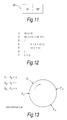
- FIG. 11 Another embodiment of the present invention can provide a processor having two or more register renaming modes.
- the processor may be provided with a mode register having first and second mode bits M1 and M2 used for registering a currently-selected register renaming mode.
- the mode register 40 may be provided in the register renaming unit 32 in Fig. 9, for example.
- the first mode bit M1 is used to control whether register renaming is enabled or disabled.
- the second mode bit M2 is effective only when the first mode bit M1 indicates that register renaming is enabled. In this case the second mode bit M2 is used to control which of two available register renaming modes is to be used.
- One of these two available modes is the mode described with reference to Table 2 and Figs.
- the other available register renaming mode may be any other suitable register renaming mode.
- the other available mode may be previously-considered mode described with reference to Figs. 5, 6(A) and 6(B) in which the registers are renamed each time a software pipeline boundary is crossed, i.e. every II processor cycles, where II is the above-mentioned loop initiation interval.
- the first mode bit M1 can be omitted.
- the second mode bit M2 may be omitted.
- the or each mode bit may be changed dynamically at execution time, for example under program control.
- This optional enhancement is intended to overcome a possible register location inconsistency which can arise in the special case in which a loop body of a software-pipelined loop is not executed at all, as compared to the normal case in which the loop body is executed one or more times.
- This special case in which the loop body of a software-pipeline loop is not executed at all can arise, for example, when a loop instruction sets up a loop to iterate whilst a loop control variable is changed incrementally from a start value to an end value, but the end value is itself a variable which, at the time the loop instruction is encountered during execution, is less than the start value.
- This special case results in register locations that are inconsistent with those which follow when the loop body is executed one or more times, as will now be explained.
- the final iteration of the loop requires that the loop schedule be issued p times. Hence, between the start of the final iteration and the final exit from the loop there will be pv rotations of the loop. If any value is live on entry to the loop and live on exit from the loop, then there must be at least pv rotating registers.
- a recurrence Any value produced in one iteration of the loop that is computed as a function of itself in a previous iteration is called a recurrence.
- Such recurrences are initialised prior to loop entry and are then used after the loop has completed.
- a scalar variable s is initialised (line 1) prior to the entry into the loop, has a recurrence within the loop body (line 4) and is also used after the loop has completed (line 7). Its lifetime therefore spans the entire loop.
- the compiler will arrange that in each iteration the code at line 4 will read the value of s produced in the previous iteration from logical register number S R and write the new value s produced in the current iteration in logical register number S W .
- These register numbers are chosen such that after rotating the register file v times the value written to register S W in the previous iteration is now available in register S R in the current iteration.
- the initial value of s which is defined at line 1 in Fig. 12, must be written to an appropriate register S 1 and S 1 must be chosen such that when the first iteration reads from S R in line 4 the value written to S 1 in line 1 has rotated such that it is now accessible in register S R .
- the precise number of rotations between line 1 and line 4 in the first iteration depends on the software pipeline stage in which line 4 occurs and on the position of the instruction which uses s within the loop schedule. Let the number of rotations required to move the value in S 1 to S R be q.
- Fig. 13 The relationship between these registers S 1 , S W , S R and S E is represented schematically in Fig. 13.
- the circle represents the rotating region of the register file.
- the size of the rotating region i.e. the circumference in Fig. 13
- pv registers which is the number of registers needed when there is at least one live-in value that is also live-out.
- the individual registers in the rotating region are spaced apart at equal intervals around the circumference.
- the processor is arranged that, if the loop iteration count is found to be zero at execution time, and hence the loop body is not to be executed at all, then the register file is rotated v(p-1) times before the processor continues past the end of the loop.
- This has the effect of skipping v(p-1) sequence numbers before issuance of a first instruction after exit from the loop. This can conveniently be achieved by issuing the instructions of the loop schedule p-1 times without actually performing the instructions.
- the act of issuing each value-producing instruction will rotate the register file, so each complete issue of the loop schedule will rotate the register file v times. In this way, when the loop iteration count is zero, the initial value of s is made available in logical register S 1 +v(p-1), as desired.
- Issuance of the instructions p-1 times can be achieved by effecting going straight into a shut-down mode of the software-pipelined loop, and setting an additional (global) predicate false to prevent any of the instructions being executed.
- the enhancement described above does cause the processor to have to take special action at execution time in a case in which the loop iteration count is zero. However, this is normally an improbable occurrence, so the typical execution-time penalty will be small.
- the enhancement is also applicable when other register renaming techniques are used, for example the previously-considered technique described with reference to Figs. 5, 6(A) and 6(B).
- the processor is arranged to rotate the registers by p-1 registers in the event of a zero iteration count.
- another aspect of the present invention can provide a processor which renames the renameable registers each time a software-pipeline boundary is crossed (instead of each time a value-producing instruction is issued) and which skips one or more renameable registers in the event of a zero iteration count.
- the number of skipped registers is independent of the number of value-producing instructions, and dependent on the number of software-pipeline stages.
- the number of skipped registers is p-1.
- each value-requiring instruction need not be a sequence offset. It would be possible to specify the identity of the register holding the required value using its assigned sequence number directly or relative to some reference point other than the sequence number currently reached. Similarly, in a value-producing instruction information dependent on the assigned sequence number could be specified to make the register allocation more flexible. For example, a sequence offset (e.g. "@-2") could be specified, to denote a logical register number other than 0 for storing the produced value. Also, the destination register could be specified explicitly based on the assigned sequence number.
- a sequence offset e.g. "@-2”
- the destination register could be specified explicitly based on the assigned sequence number.
- sequence numbers assignable to the produced values may have a limit value, e.g. 255, so that the sequence starts from 0 again after reaching the limit value.
- a processor embodying the present invention may be included as a processor "core" in a highly-integrated "system-on-a-chip” (SOC) for use in multimedia applications, network routers, video mobile phones, intelligent automobiles, digital television, voice recognition, 3D games, etc.
- SOC system-on-a-chip
Landscapes
- Engineering & Computer Science (AREA)
- Theoretical Computer Science (AREA)
- Software Systems (AREA)
- General Engineering & Computer Science (AREA)
- Physics & Mathematics (AREA)
- General Physics & Mathematics (AREA)
- Devices For Executing Special Programs (AREA)
- Advance Control (AREA)
- Executing Machine-Instructions (AREA)
Applications Claiming Priority (2)
| Application Number | Priority Date | Filing Date | Title |
|---|---|---|---|
| GB0002848 | 2000-02-08 | ||
| GBGB0002848.0A GB0002848D0 (en) | 2000-02-08 | 2000-02-08 | Communicating instruction results in processors and compiling methods for processors |
Publications (2)
| Publication Number | Publication Date |
|---|---|
| EP1124182A2 true EP1124182A2 (de) | 2001-08-16 |
| EP1124182A3 EP1124182A3 (de) | 2005-08-03 |
Family
ID=9885153
Family Applications (1)
| Application Number | Title | Priority Date | Filing Date |
|---|---|---|---|
| EP01300947A Withdrawn EP1124182A3 (de) | 2000-02-08 | 2001-02-02 | Übertragung von Ergebnissen in einem Prozessor, und Verfahren zur Kompilierung |
Country Status (5)
| Country | Link |
|---|---|
| US (1) | US6826677B2 (de) |
| EP (1) | EP1124182A3 (de) |
| JP (1) | JP2001282532A (de) |
| CN (1) | CN1308274A (de) |
| GB (2) | GB0002848D0 (de) |
Cited By (1)
| Publication number | Priority date | Publication date | Assignee | Title |
|---|---|---|---|---|
| EP1785857A2 (de) | 2005-11-09 | 2007-05-16 | Samsung Electronics Co., Ltd. | Datenverarbeitungssystem und Verfahren |
Families Citing this family (54)
| Publication number | Priority date | Publication date | Assignee | Title |
|---|---|---|---|---|
| SE0002440D0 (sv) | 2000-06-28 | 2000-06-28 | Virtutech Ab | Interpreter |
| GB2398411B (en) | 2001-10-12 | 2005-04-27 | Pts Corp | Processors and compiling methods for processors |
| CA2365375A1 (en) * | 2001-12-18 | 2003-06-18 | Ibm Canada Limited-Ibm Canada Limitee | Optimizing source code for iterative execution |
| US7200738B2 (en) | 2002-04-18 | 2007-04-03 | Micron Technology, Inc. | Reducing data hazards in pipelined processors to provide high processor utilization |
| US20030237080A1 (en) * | 2002-06-19 | 2003-12-25 | Carol Thompson | System and method for improved register allocation in an optimizing compiler |
| US7058938B2 (en) * | 2003-03-05 | 2006-06-06 | Intel Corporation | Method and system for scheduling software pipelined loops |
| JP2005129001A (ja) * | 2003-09-30 | 2005-05-19 | Toshiba Corp | プログラム実行装置、マイクロプロセッサ及びプログラム実行方法 |
| US7493481B1 (en) * | 2004-05-17 | 2009-02-17 | Netxen, Inc. | Direct hardware processing of internal data structure fields |
| US7673294B2 (en) * | 2005-01-18 | 2010-03-02 | Texas Instruments Incorporated | Mechanism for pipelining loops with irregular loop control |
| US7761691B2 (en) * | 2005-10-27 | 2010-07-20 | National Tsing Hua University | Method for allocating registers using simulated annealing controlled instruction scheduling |
| US7840954B2 (en) * | 2005-11-29 | 2010-11-23 | International Business Machines Corporation | Compilation for a SIMD RISC processor |
| EP2011018B1 (de) | 2006-04-12 | 2016-07-13 | Soft Machines, Inc. | Vorrichtung und verfahren zur verarbeitung einer instruktionsmatrix zur definition paralleler und abhängiger operationen |
| CN107368285B (zh) * | 2006-11-14 | 2020-10-09 | 英特尔公司 | 多线程架构 |
| US7809930B2 (en) * | 2007-01-24 | 2010-10-05 | Arm Limited | Selective suppression of register renaming |
| US8413151B1 (en) | 2007-12-19 | 2013-04-02 | Nvidia Corporation | Selective thread spawning within a multi-threaded processing system |
| US8615770B1 (en) | 2008-08-29 | 2013-12-24 | Nvidia Corporation | System and method for dynamically spawning thread blocks within multi-threaded processing systems |
| US8959497B1 (en) * | 2008-08-29 | 2015-02-17 | Nvidia Corporation | System and method for dynamically spawning thread blocks within multi-threaded processing systems |
| CN101770387B (zh) * | 2008-12-26 | 2013-03-13 | 北京中电华大电子设计有限责任公司 | 一种含有配对寄存器的寄存器分配方法 |
| CN101894013B (zh) * | 2010-07-16 | 2013-07-31 | 中国科学院计算技术研究所 | 处理器内指令级流水线控制方法及其系统 |
| EP3156896B1 (de) | 2010-09-17 | 2020-04-08 | Soft Machines, Inc. | Mehrfach verzweigte einzelzyklusvorhersage mit einem latenten cache für frühe und entfernte verzweigungsvorhersage |
| CN103547993B (zh) | 2011-03-25 | 2018-06-26 | 英特尔公司 | 通过使用由可分割引擎实例化的虚拟核来执行指令序列代码块 |
| CN108108188B (zh) | 2011-03-25 | 2022-06-28 | 英特尔公司 | 用于通过使用由可分区引擎实例化的虚拟核来支持代码块执行的存储器片段 |
| KR101620676B1 (ko) | 2011-03-25 | 2016-05-23 | 소프트 머신즈, 인크. | 분할가능한 엔진에 의해 인스턴스화된 가상 코어를 이용한 코드 블록의 실행을 지원하는 레지스터 파일 세그먼트 |
| CN107729267B (zh) | 2011-05-20 | 2022-01-25 | 英特尔公司 | 资源的分散分配以及用于支持由多个引擎执行指令序列的互连结构 |
| US9442772B2 (en) | 2011-05-20 | 2016-09-13 | Soft Machines Inc. | Global and local interconnect structure comprising routing matrix to support the execution of instruction sequences by a plurality of engines |
| KR101703401B1 (ko) | 2011-11-22 | 2017-02-06 | 소프트 머신즈, 인크. | 다중 엔진 마이크로프로세서용 가속 코드 최적화기 |
| WO2013077876A1 (en) | 2011-11-22 | 2013-05-30 | Soft Machines, Inc. | A microprocessor accelerated code optimizer |
| CN104321747B (zh) * | 2012-04-19 | 2017-11-17 | 西门子公司 | 用于多核/众核可编程逻辑控制器的时间裕隙应用流水线平衡 |
| US9569216B2 (en) | 2013-03-15 | 2017-02-14 | Soft Machines, Inc. | Method for populating a source view data structure by using register template snapshots |
| WO2014151043A1 (en) | 2013-03-15 | 2014-09-25 | Soft Machines, Inc. | A method for emulating a guest centralized flag architecture by using a native distributed flag architecture |
| WO2014150806A1 (en) | 2013-03-15 | 2014-09-25 | Soft Machines, Inc. | A method for populating register view data structure by using register template snapshots |
| WO2014150971A1 (en) | 2013-03-15 | 2014-09-25 | Soft Machines, Inc. | A method for dependency broadcasting through a block organized source view data structure |
| US10275255B2 (en) | 2013-03-15 | 2019-04-30 | Intel Corporation | Method for dependency broadcasting through a source organized source view data structure |
| US9886279B2 (en) | 2013-03-15 | 2018-02-06 | Intel Corporation | Method for populating and instruction view data structure by using register template snapshots |
| US9904625B2 (en) | 2013-03-15 | 2018-02-27 | Intel Corporation | Methods, systems and apparatus for predicting the way of a set associative cache |
| US10140138B2 (en) | 2013-03-15 | 2018-11-27 | Intel Corporation | Methods, systems and apparatus for supporting wide and efficient front-end operation with guest-architecture emulation |
| US9811342B2 (en) | 2013-03-15 | 2017-11-07 | Intel Corporation | Method for performing dual dispatch of blocks and half blocks |
| WO2014150991A1 (en) | 2013-03-15 | 2014-09-25 | Soft Machines, Inc. | A method for implementing a reduced size register view data structure in a microprocessor |
| US9891924B2 (en) | 2013-03-15 | 2018-02-13 | Intel Corporation | Method for implementing a reduced size register view data structure in a microprocessor |
| EP2972845B1 (de) | 2013-03-15 | 2021-07-07 | Intel Corporation | Verfahren zur ausführung von in blöcken gruppierten befehlen aus mehreren threads |
| CN105164637B (zh) * | 2013-05-30 | 2017-12-19 | 英特尔公司 | 用于执行循环的方法、系统、装置和处理器以及机器可读介质 |
| AU2013387185B2 (en) * | 2013-05-30 | 2016-08-04 | Intel Corporation | Allocation of alias registers in a pipelined schedule |
| US9424011B2 (en) * | 2014-04-01 | 2016-08-23 | International Business Machines Corporation | Recursive expression simplification |
| US9841974B2 (en) * | 2014-04-25 | 2017-12-12 | Avago Technologies General Ip (Singapore) Pte. Ltd. | Renaming with generation numbers |
| US9740411B2 (en) * | 2014-09-04 | 2017-08-22 | National Instruments Corporation | Configuring circuitry with memory access constraints for a program |
| GB2539410B (en) | 2015-06-15 | 2017-12-06 | Bluwireless Tech Ltd | Data processing |
| GB2539411B (en) | 2015-06-15 | 2017-06-28 | Bluwireless Tech Ltd | Data processing |
| CN105354117B (zh) * | 2015-10-26 | 2018-10-19 | 清华大学 | 超标量处理器中指令相关性检测的方法 |
| CN106293627B (zh) * | 2016-07-27 | 2019-01-11 | 珠海市杰理科技股份有限公司 | 寄存器调用及调用指令编码的方法、装置 |
| CN109188994B (zh) * | 2017-06-30 | 2021-06-08 | 沈阳新松机器人自动化股份有限公司 | 一种梯形图编译方法及相应的plc系统 |
| CN108052347B (zh) * | 2017-12-06 | 2021-07-20 | 北京中科睿芯智能计算产业研究院有限公司 | 一种执行指令选择的装置、方法及指令映射方法 |
| US11366646B2 (en) * | 2020-01-23 | 2022-06-21 | Huawei Technologies Co., Ltd. | Method and apparatus for predicting and scheduling copy instruction for software pipelined loops |
| US12182554B2 (en) * | 2022-09-09 | 2024-12-31 | Microsoft Technology Licensing, Llc. | Interleaved machine instruction placement in memory |
| CN116400982B (zh) * | 2023-05-26 | 2023-08-08 | 摩尔线程智能科技(北京)有限责任公司 | 配置中继寄存器模块的方法和装置、计算设备和可读介质 |
Family Cites Families (7)
| Publication number | Priority date | Publication date | Assignee | Title |
|---|---|---|---|---|
| US5826055A (en) * | 1991-07-08 | 1998-10-20 | Seiko Epson Corporation | System and method for retiring instructions in a superscalar microprocessor |
| US5628021A (en) * | 1992-12-31 | 1997-05-06 | Seiko Epson Corporation | System and method for assigning tags to control instruction processing in a superscalar processor |
| GB9305263D0 (en) * | 1993-03-15 | 1993-05-05 | Univ Westminster | Parrallel computation |
| US6205538B1 (en) * | 1994-08-24 | 2001-03-20 | Sun Microsystems, Inc. | Instruction result labeling in a counterflow pipeline processor |
| US5911057A (en) * | 1995-12-19 | 1999-06-08 | Texas Instruments Incorporated | Superscalar microprocessor having combined register and memory renaming circuits, systems, and methods |
| JP2933026B2 (ja) * | 1996-08-30 | 1999-08-09 | 日本電気株式会社 | 複数命令並列発行/実行管理装置 |
| GB2317464A (en) * | 1996-09-23 | 1998-03-25 | Advanced Risc Mach Ltd | Register addressing in a data processing apparatus |
-
2000
- 2000-02-08 GB GBGB0002848.0A patent/GB0002848D0/en not_active Ceased
-
2001
- 2001-01-31 GB GB0102461A patent/GB2355094B/en not_active Expired - Fee Related
- 2001-02-02 EP EP01300947A patent/EP1124182A3/de not_active Withdrawn
- 2001-02-06 US US09/777,755 patent/US6826677B2/en not_active Expired - Lifetime
- 2001-02-08 JP JP2001032090A patent/JP2001282532A/ja active Pending
- 2001-02-08 CN CN01103251A patent/CN1308274A/zh active Pending
Cited By (3)
| Publication number | Priority date | Publication date | Assignee | Title |
|---|---|---|---|---|
| EP1785857A2 (de) | 2005-11-09 | 2007-05-16 | Samsung Electronics Co., Ltd. | Datenverarbeitungssystem und Verfahren |
| EP1785857A3 (de) * | 2005-11-09 | 2009-01-28 | Samsung Electronics Co., Ltd. | Datenverarbeitungssystem und Verfahren |
| US7660970B2 (en) | 2005-11-09 | 2010-02-09 | Samsung Electronics Co., Ltd. | Register allocation method and system for program compiling |
Also Published As
| Publication number | Publication date |
|---|---|
| US20010016901A1 (en) | 2001-08-23 |
| US6826677B2 (en) | 2004-11-30 |
| CN1308274A (zh) | 2001-08-15 |
| GB2355094A (en) | 2001-04-11 |
| GB0102461D0 (en) | 2001-03-14 |
| EP1124182A3 (de) | 2005-08-03 |
| GB0002848D0 (en) | 2000-03-29 |
| JP2001282532A (ja) | 2001-10-12 |
| GB2355094B (en) | 2002-05-01 |
Similar Documents
| Publication | Publication Date | Title |
|---|---|---|
| US6826677B2 (en) | Renaming registers to values produced by instructions according to assigned produce sequence number | |
| US6944853B2 (en) | Predicated execution of instructions in processors | |
| US5303357A (en) | Loop optimization system | |
| US5367651A (en) | Integrated register allocation, instruction scheduling, instruction reduction and loop unrolling | |
| JP2928695B2 (ja) | 静的インタリーブを用いたマルチスレッドマイクロプロセッサおよびそれを備えたシステムでの命令スレッド実行方法 | |
| US11720332B2 (en) | Compiling a program from a graph | |
| US7631305B2 (en) | Methods and products for processing loop nests | |
| US20140223142A1 (en) | Processor and compiler | |
| US7512771B2 (en) | Mapping circuitry and method comprising first and second candidate output value producing units, an in-range value determining unit, and an output value selection unit | |
| KR20150059894A (ko) | 다수의 기능 유닛을 가지는 프로세서를 위한 루프 스케쥴링 방법 | |
| US6738893B1 (en) | Method and apparatus for scheduling to reduce space and increase speed of microprocessor operations | |
| JPH11194948A (ja) | コンパイラ最適化アルゴリズム | |
| GB2394085A (en) | Generating code for a configurable microprocessor | |
| US7130989B2 (en) | Processor adapted to receive different instruction sets | |
| US7316012B2 (en) | System, method, and apparatus for spilling and filling rotating registers in software-pipelined loops | |
| JP2002251282A (ja) | プロセッサにおけるループの処理 | |
| CN115004150A (zh) | 用于预测和调度软件流水化循环中的复制指令的方法和装置 | |
| US11762641B2 (en) | Allocating variables to computer memory | |
| JP7383390B2 (ja) | 情報処理ユニット、情報処理装置、情報処理方法及びプログラム | |
| US8549466B2 (en) | Tiered register allocation | |
| US11675572B2 (en) | Sharing data structures | |
| Kästner et al. | Integer linear programming vs. graph-based methods in code generation | |
| Rubanov et al. | Specific optimization features in a C compiler for DSPs | |
| JPH1153197A (ja) | ループ最適化方法 |
Legal Events
| Date | Code | Title | Description |
|---|---|---|---|
| PUAI | Public reference made under article 153(3) epc to a published international application that has entered the european phase |
Free format text: ORIGINAL CODE: 0009012 |
|
| AK | Designated contracting states |
Kind code of ref document: A2 Designated state(s): AT BE CH CY DE DK ES FI FR GB GR IE IT LI LU MC NL PT SE TR |
|
| AX | Request for extension of the european patent |
Free format text: AL;LT;LV;MK;RO;SI |
|
| RAP1 | Party data changed (applicant data changed or rights of an application transferred) |
Owner name: PTS CORPORATION |
|
| PUAL | Search report despatched |
Free format text: ORIGINAL CODE: 0009013 |
|
| AK | Designated contracting states |
Kind code of ref document: A3 Designated state(s): AT BE CH CY DE DK ES FI FR GB GR IE IT LI LU MC NL PT SE TR |
|
| AX | Request for extension of the european patent |
Extension state: AL LT LV MK RO SI |
|
| RIC1 | Information provided on ipc code assigned before grant |
Ipc: 7G 06F 9/45 A |
|
| 17P | Request for examination filed |
Effective date: 20060125 |
|
| AKX | Designation fees paid |
Designated state(s): DE GB |
|
| RAP1 | Party data changed (applicant data changed or rights of an application transferred) |
Owner name: ALTERA CORPORATION |
|
| GRAP | Despatch of communication of intention to grant a patent |
Free format text: ORIGINAL CODE: EPIDOSNIGR1 |
|
| STAA | Information on the status of an ep patent application or granted ep patent |
Free format text: STATUS: THE APPLICATION IS DEEMED TO BE WITHDRAWN |
|
| 18D | Application deemed to be withdrawn |
Effective date: 20080304 |