EP1124231A1 - Circuit mémoire avec un temps d'accès plus court - Google Patents
Circuit mémoire avec un temps d'accès plus court Download PDFInfo
- Publication number
- EP1124231A1 EP1124231A1 EP01100894A EP01100894A EP1124231A1 EP 1124231 A1 EP1124231 A1 EP 1124231A1 EP 01100894 A EP01100894 A EP 01100894A EP 01100894 A EP01100894 A EP 01100894A EP 1124231 A1 EP1124231 A1 EP 1124231A1
- Authority
- EP
- European Patent Office
- Prior art keywords
- local data
- data line
- strips
- memory chip
- memory
- Prior art date
- Legal status (The legal status is an assumption and is not a legal conclusion. Google has not performed a legal analysis and makes no representation as to the accuracy of the status listed.)
- Withdrawn
Links
- 230000001360 synchronised effect Effects 0.000 claims description 8
- 230000003213 activating effect Effects 0.000 description 2
- 230000004913 activation Effects 0.000 description 2
- 230000007774 longterm Effects 0.000 description 2
- 230000003247 decreasing effect Effects 0.000 description 1
- 238000011161 development Methods 0.000 description 1
- 230000018109 developmental process Effects 0.000 description 1
Images

Classifications
-
- G—PHYSICS
- G11—INFORMATION STORAGE
- G11C—STATIC STORES
- G11C7/00—Arrangements for writing information into, or reading information out from, a digital store
- G11C7/12—Bit line control circuits, e.g. drivers, boosters, pull-up circuits, pull-down circuits, precharging circuits, equalising circuits, for bit lines
-
- G—PHYSICS
- G11—INFORMATION STORAGE
- G11C—STATIC STORES
- G11C7/00—Arrangements for writing information into, or reading information out from, a digital store
- G11C7/10—Input/output [I/O] data interface arrangements, e.g. I/O data control circuits, I/O data buffers
- G11C7/1051—Data output circuits, e.g. read-out amplifiers, data output buffers, data output registers, data output level conversion circuits
- G11C7/1069—I/O lines read out arrangements
Definitions
- the invention relates to a memory chip according to the Preamble of claim 1.
- the access time, both when reading and when So storing bits is needed is a size whose Value should be as low as possible.
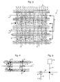
- the Cell field 1 consists of several cell field strips 2 which by parallel to the cell field strips 2, on both sides adjacent local data line strips 3 from each other are separated.
- the cell field strips 2 consist of essentially from a variety of memory cells 7.
- the Local data line strips 3 have several local ones Data lines 4 on.
- the cell field 1 also has Power amplifier 6, to each of which a main data line 5 connected. This main data line 5 runs perpendicular to both the cell field strips 2 and local data strip 3.
- Word lines 11 which are parallel to the local Data line strip 3 and within a certain Cell field strip 2 run, provided.
- column lines 12 which are parallel to the Main data lines 5 run and the word lines 11 in Cut intersection points 13, provided.
- Each Memory cell 7 can be one of the Assign crossing points 13. The activation of a Crossing point 13 is done by activating the corresponding word and column line 11, 12. Is the Crossing point 13 activated, so the assigned Memory cells 7 can be accessed.
- Fig. 5 shows a schematic representation of the path that a Bit travels when it is read from a memory chip is written or written to a memory block.
- An in a memory cell 7 is stored bit after it over a word line 11 and a column line 12 (see FIG. 4) was activated via a bit line 8 to one Brought preamplifier 9, which on a local Data line 4 of a local data line strip 3 is attached and a connecting link between bit line 8 and local data line 4. That through the Pre-amplified bit then passes through the local one Data line 4 to a switch 10, which on a Main data line 5 is and a connecting link between represents local data line 4 and main data line 5.
- This switch 10 passes the signal on Main data line 5 to a power amplifier 6, which raises the signal to a desired output level and then forwards to an output of the memory chip.
- the object underlying the invention is a Memory chip according to the prior art to further develop that access time to a desired one Amount of bits is minimized with a synchronous access.
- This task is the beginning of a memory chip mentioned type according to the invention solved in that the Switches are arranged so that the longest possible The runtime of a bit in the local data lines is all the shorter is, the further the local data lines are relative to the others with synchronous memory access at the same time required local data lines from the power amplifiers are removed.
- the main idea of the present invention is that to design individual paths of the individual bits in such a way that individual paths with a long runtime are avoided. To compensate, the path length of the individual paths is included short term increased.
- the extensive equal distribution the number of individual routes with short, medium and long term is redistributed into a small number individual ways with short and long term as well as a high number of individual routes with medium duration.
- Another feature of the present invention is that the design of the individual routes preferably via the Arrangement of the switches on the local data line strips, which consist of local data lines.
- the length of the individual can be determined by the position of the switch Way the bit on the local data line strip covered, specifically changed.
- the arrangement of the Switch on a local data line strip, which relative to the others for synchronous memory access local data line strips required at the same time It is farthest from the power amplifiers designed so that these switches as far as possible in the middle of the local data line strip. About that can maximum signal paths and thus maximum Runtimes on the local data lines are avoided, because then at most half a length of the local Data line strip must be traversed.
- Fig. 1 shows a particularly preferred embodiment of a memory device according to the invention.
- This memory chip is designed for synchronous access to sixteen bits.
- Each two switches 10, which are on the same local Data line strips 14, 15, 16, 17, 18 lie from an axis 19 of the memory chip an equal distance 20 on.
- This arrangement structure can, for example, with increasing distance from the power amplifiers 6 periodically repeat and can also be transferred to memory modules, which have synchronous access to more or less than sixteen bits, for example thirty-two bits.
Landscapes
- Dram (AREA)
- Semiconductor Memories (AREA)
Applications Claiming Priority (2)
| Application Number | Priority Date | Filing Date | Title |
|---|---|---|---|
| DE10004109 | 2000-01-31 | ||
| DE10004109A DE10004109C2 (de) | 2000-01-31 | 2000-01-31 | Speicherbaustein mit geringer Zugriffszeit |
Publications (1)
| Publication Number | Publication Date |
|---|---|
| EP1124231A1 true EP1124231A1 (fr) | 2001-08-16 |
Family
ID=7629300
Family Applications (1)
| Application Number | Title | Priority Date | Filing Date |
|---|---|---|---|
| EP01100894A Withdrawn EP1124231A1 (fr) | 2000-01-31 | 2001-01-16 | Circuit mémoire avec un temps d'accès plus court |
Country Status (6)
| Country | Link |
|---|---|
| US (1) | US6388944B2 (fr) |
| EP (1) | EP1124231A1 (fr) |
| JP (1) | JP3957977B2 (fr) |
| KR (1) | KR100392317B1 (fr) |
| DE (1) | DE10004109C2 (fr) |
| TW (1) | TW502259B (fr) |
Families Citing this family (11)
| Publication number | Priority date | Publication date | Assignee | Title |
|---|---|---|---|---|
| US6809914B2 (en) | 2002-05-13 | 2004-10-26 | Infineon Technologies Ag | Use of DQ pins on a ram memory chip for a temperature sensing protocol |
| US6873509B2 (en) | 2002-05-13 | 2005-03-29 | Infineon Technologies Ag | Use of an on-die temperature sensing scheme for thermal protection of DRAMS |
| US6711091B1 (en) | 2002-09-27 | 2004-03-23 | Infineon Technologies Ag | Indication of the system operation frequency to a DRAM during power-up |
| US6985400B2 (en) | 2002-09-30 | 2006-01-10 | Infineon Technologies Ag | On-die detection of the system operation frequency in a DRAM to adjust DRAM operations |
| DE10345550B3 (de) * | 2003-09-30 | 2005-02-10 | Infineon Technologies Ag | Speicheranordnung mit mehreren RAM-Bausteinen |
| KR100873623B1 (ko) * | 2007-07-10 | 2008-12-12 | 주식회사 하이닉스반도체 | 반도체 메모리 장치 |
| US8171135B2 (en) * | 2007-07-12 | 2012-05-01 | Viasat, Inc. | Accumulator for prefetch abort |
| US20100146415A1 (en) * | 2007-07-12 | 2010-06-10 | Viasat, Inc. | Dns prefetch |
| US8549099B2 (en) * | 2007-07-12 | 2013-10-01 | Viasat, Inc. | Methods and systems for javascript parsing |
| US20100180082A1 (en) * | 2009-01-12 | 2010-07-15 | Viasat, Inc. | Methods and systems for implementing url masking |
| RU2510531C1 (ru) * | 2009-12-31 | 2014-03-27 | Наутилус Хесун Инк. | Банковский автомат |
Citations (2)
| Publication number | Priority date | Publication date | Assignee | Title |
|---|---|---|---|---|
| US5781495A (en) * | 1996-07-23 | 1998-07-14 | Mitsubishi Denki Kabushiki Kaisha | Semiconductor memory device for multi-bit or multi-bank architectures |
| US5982698A (en) * | 1998-07-14 | 1999-11-09 | Mitsubishi Denki Kabushiki Kaisha | Multi-bank system semiconductor memory device capable of operating at high speed |
Family Cites Families (4)
| Publication number | Priority date | Publication date | Assignee | Title |
|---|---|---|---|---|
| US5636158A (en) * | 1995-03-13 | 1997-06-03 | Kabushiki Kaisha Toshiba | Irregular pitch layout for a semiconductor memory device |
| JPH08263985A (ja) * | 1995-03-24 | 1996-10-11 | Nec Corp | 半導体記憶装置 |
| US5966315A (en) * | 1997-09-30 | 1999-10-12 | Siemens Aktiengesellschaft | Semiconductor memory having hierarchical bit line architecture with non-uniform local bit lines |
| JP2000048566A (ja) * | 1998-07-29 | 2000-02-18 | Mitsubishi Electric Corp | 同期型半導体記憶装置 |
-
2000
- 2000-01-31 DE DE10004109A patent/DE10004109C2/de not_active Expired - Fee Related
-
2001
- 2001-01-16 EP EP01100894A patent/EP1124231A1/fr not_active Withdrawn
- 2001-01-30 JP JP2001021717A patent/JP3957977B2/ja not_active Expired - Fee Related
- 2001-01-30 TW TW090101790A patent/TW502259B/zh not_active IP Right Cessation
- 2001-01-31 KR KR10-2001-0004519A patent/KR100392317B1/ko not_active Expired - Fee Related
- 2001-01-31 US US09/773,221 patent/US6388944B2/en not_active Expired - Lifetime
Patent Citations (2)
| Publication number | Priority date | Publication date | Assignee | Title |
|---|---|---|---|---|
| US5781495A (en) * | 1996-07-23 | 1998-07-14 | Mitsubishi Denki Kabushiki Kaisha | Semiconductor memory device for multi-bit or multi-bank architectures |
| US5982698A (en) * | 1998-07-14 | 1999-11-09 | Mitsubishi Denki Kabushiki Kaisha | Multi-bank system semiconductor memory device capable of operating at high speed |
Also Published As
| Publication number | Publication date |
|---|---|
| TW502259B (en) | 2002-09-11 |
| KR20010078194A (ko) | 2001-08-20 |
| DE10004109C2 (de) | 2001-11-29 |
| KR100392317B1 (ko) | 2003-07-22 |
| US6388944B2 (en) | 2002-05-14 |
| JP2001256780A (ja) | 2001-09-21 |
| US20010038566A1 (en) | 2001-11-08 |
| DE10004109A1 (de) | 2001-08-09 |
| JP3957977B2 (ja) | 2007-08-15 |
Similar Documents
| Publication | Publication Date | Title |
|---|---|---|
| DE112020006398T5 (de) | Geräte, systeme und verfahren zur fehlerkorrektur | |
| DE4220211C2 (de) | Spaltenauswahlschaltung | |
| DE2364785A1 (de) | Integrierter halbleiterspeicher mit defekten speicherzellen | |
| DE69020384T2 (de) | Integrierte Halbleiterspeicherschaltung mit Möglichkeit zum Maskieren des Schreibens im Speicher. | |
| DE10063631A1 (de) | Virtueller Kanal in Synchronisation mit einem dynamischen Ram-Speicher | |
| DE4006285C2 (fr) | ||
| DE3940302C2 (fr) | ||
| DE3618136C2 (fr) | ||
| DE10004109C2 (de) | Speicherbaustein mit geringer Zugriffszeit | |
| DE69222743T2 (de) | Speichereinrichtung und Verfahren zur Verwendung in einer Datenverarbeitungsanordnung | |
| DE19680641C2 (de) | Fehlerspeicher-Analysiervorrichtung in einem Halbleiterspeichertestsystem | |
| DE69525527T2 (de) | Multiport mehrfachregisterspeicher zum empfang von daten unterschiedlicher länge | |
| EP1205938B1 (fr) | Circuit intégré avec mode test et procédé pour le test d'une pluralité desdits circuits | |
| DE4312086A1 (de) | Halbleiterspeichereinrichtung und Betriebsverfahren dafür | |
| DE69614947T2 (de) | Halbleiterspeicheranordnung mit einer Schaltungsanordnungstruktur für hohe Geschwindigkeit | |
| DE69412234T2 (de) | Redundanzschaltung für eine Halbleiter-Speicheranordnung | |
| DE19922786B4 (de) | Halbleiterspeicher mit Testeinrichtung | |
| EP1118999A1 (fr) | Procédé et système pour utiliser une mémoire à accés en rafale dans un mode de travail avec une mémoire et un autre mode avec plusieurs mémoires | |
| DE19944738A1 (de) | Segmentierte Wortleitungsarchitektur zur Aufteilung einer Wortleitung in mehrere Bänke für Zellenfelder mit langen Bitleitungen | |
| DE3138897A1 (de) | Schaltungsanordnung zur verarbeitung von speicheroperanden fuer dezimale und logische befehle | |
| DE69523481T2 (de) | Technik zum rekonfigurieren eines speichers hoher dichte | |
| DE10307027A1 (de) | Verfahren und Testeinrichtung zum Ermitteln einer Reparaturlösung für einen Speicherbaustein | |
| DE10226485A1 (de) | Halbleiterspeicher mit Adressdecodiereinheit | |
| DE10063732B4 (de) | Halbleiterspeicherbauelement mit hierarchischer Wortleitungsstruktur | |
| DE10147201A1 (de) | Halbleiterspeichervorrichtung und Verfahren zum Ersetzen einer Redundanzschaltung |
Legal Events
| Date | Code | Title | Description |
|---|---|---|---|
| PUAI | Public reference made under article 153(3) epc to a published international application that has entered the european phase |
Free format text: ORIGINAL CODE: 0009012 |
|
| AK | Designated contracting states |
Kind code of ref document: A1 Designated state(s): AT BE CH CY DE DK ES FI FR GB GR IE IT LI LU MC NL PT SE TR |
|
| AX | Request for extension of the european patent |
Free format text: AL;LT;LV;MK;RO;SI |
|
| AKX | Designation fees paid | ||
| REG | Reference to a national code |
Ref country code: DE Ref legal event code: 8566 |
|
| STAA | Information on the status of an ep patent application or granted ep patent |
Free format text: STATUS: THE APPLICATION IS DEEMED TO BE WITHDRAWN |
|
| 18D | Application deemed to be withdrawn |
Effective date: 20020513 |