EP1124256A1 - Substrat en ceramique - Google Patents
Substrat en ceramique Download PDFInfo
- Publication number
- EP1124256A1 EP1124256A1 EP00902967A EP00902967A EP1124256A1 EP 1124256 A1 EP1124256 A1 EP 1124256A1 EP 00902967 A EP00902967 A EP 00902967A EP 00902967 A EP00902967 A EP 00902967A EP 1124256 A1 EP1124256 A1 EP 1124256A1
- Authority
- EP
- European Patent Office
- Prior art keywords
- ceramic substrate
- hole
- green sheet
- projection
- ceramic
- Prior art date
- Legal status (The legal status is an assumption and is not a legal conclusion. Google has not performed a legal analysis and makes no representation as to the accuracy of the status listed.)
- Withdrawn
Links
Images



Classifications
-
- H—ELECTRICITY
- H10—SEMICONDUCTOR DEVICES; ELECTRIC SOLID-STATE DEVICES NOT OTHERWISE PROVIDED FOR
- H10W—GENERIC PACKAGES, INTERCONNECTIONS, CONNECTORS OR OTHER CONSTRUCTIONAL DETAILS OF DEVICES COVERED BY CLASS H10
- H10W70/00—Package substrates; Interposers; Redistribution layers [RDL]
- H10W70/60—Insulating or insulated package substrates; Interposers; Redistribution layers
- H10W70/62—Insulating or insulated package substrates; Interposers; Redistribution layers characterised by their interconnections
- H10W70/63—Vias, e.g. via plugs
- H10W70/635—Through-vias
-
- H—ELECTRICITY
- H02—GENERATION; CONVERSION OR DISTRIBUTION OF ELECTRIC POWER
- H02N—ELECTRIC MACHINES NOT OTHERWISE PROVIDED FOR
- H02N13/00—Clutches or holding devices using electrostatic attraction, e.g. using Johnson-Rahbek effect
-
- H—ELECTRICITY
- H10—SEMICONDUCTOR DEVICES; ELECTRIC SOLID-STATE DEVICES NOT OTHERWISE PROVIDED FOR
- H10P—GENERIC PROCESSES OR APPARATUS FOR THE MANUFACTURE OR TREATMENT OF DEVICES COVERED BY CLASS H10
- H10P72/00—Handling or holding of wafers, substrates or devices during manufacture or treatment thereof
- H10P72/70—Handling or holding of wafers, substrates or devices during manufacture or treatment thereof for supporting or gripping
- H10P72/72—Handling or holding of wafers, substrates or devices during manufacture or treatment thereof for supporting or gripping using electrostatic chucks
- H10P72/722—Details of electrostatic chucks
-
- Y—GENERAL TAGGING OF NEW TECHNOLOGICAL DEVELOPMENTS; GENERAL TAGGING OF CROSS-SECTIONAL TECHNOLOGIES SPANNING OVER SEVERAL SECTIONS OF THE IPC; TECHNICAL SUBJECTS COVERED BY FORMER USPC CROSS-REFERENCE ART COLLECTIONS [XRACs] AND DIGESTS
- Y10—TECHNICAL SUBJECTS COVERED BY FORMER USPC
- Y10T—TECHNICAL SUBJECTS COVERED BY FORMER US CLASSIFICATION
- Y10T428/00—Stock material or miscellaneous articles
- Y10T428/24—Structurally defined web or sheet [e.g., overall dimension, etc.]
- Y10T428/24802—Discontinuous or differential coating, impregnation or bond [e.g., artwork, printing, retouched photograph, etc.]
- Y10T428/24917—Discontinuous or differential coating, impregnation or bond [e.g., artwork, printing, retouched photograph, etc.] including metal layer
-
- Y—GENERAL TAGGING OF NEW TECHNOLOGICAL DEVELOPMENTS; GENERAL TAGGING OF CROSS-SECTIONAL TECHNOLOGIES SPANNING OVER SEVERAL SECTIONS OF THE IPC; TECHNICAL SUBJECTS COVERED BY FORMER USPC CROSS-REFERENCE ART COLLECTIONS [XRACs] AND DIGESTS
- Y10—TECHNICAL SUBJECTS COVERED BY FORMER USPC
- Y10T—TECHNICAL SUBJECTS COVERED BY FORMER US CLASSIFICATION
- Y10T428/00—Stock material or miscellaneous articles
- Y10T428/24—Structurally defined web or sheet [e.g., overall dimension, etc.]
- Y10T428/24802—Discontinuous or differential coating, impregnation or bond [e.g., artwork, printing, retouched photograph, etc.]
- Y10T428/24926—Discontinuous or differential coating, impregnation or bond [e.g., artwork, printing, retouched photograph, etc.] including ceramic, glass, porcelain or quartz layer
Definitions
- the present invention relates to a ceramic substrate for use in the semiconductor industrial field, and more particularly, it relates to a ceramic substrate for use in a wafer prober, an electrostatic chuck, a hot plate and the like, for use in the manufacture or inspection processes of semiconductors.
- semiconductor chips are manufactured by slicing a silicon monocrystalline to a predetermined thickness to produce a silicon wafer; then forming a variety of circuits in a pattern shape thereon.
- an electrostatic chuck for supporting a wafer, a hot plate for heating a wafer, and a wafer prober for checking whether the circuit operates in accordance with its design are needed.
- These may preferably be of ceramic material in terms of heat resistance and corrosion resistance.
- Japanese patent registration No. 2798570 discloses an electrostatic chuck made of ceramic materials having such construction as to have a heat generation body therein.
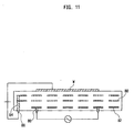
- Fig. 11 is a cross sectional view showing an example of such electrostatic chuck schematically.
- the electrostatic chuck shown in the figure is provided therein with a RF electrode 80 and a heat generation body 82. Furthermore, the electrostatic chuck is provided therein with through-holes 84, 86 for connection respectively with the RF electrode 80 and the heat generation body 82.
- respective through-holes 84, 86 are formed by a sintered ceramic body of a laminated structure, which have a cylindrical shape, and being filled with conductive components.
- the conductive materials for example, tungsten is adopted.
- the structure of the through-holes of the electrostatic chuck are such that the electric wiring of respective layers are drawn out and/or connected to each other via an external terminal pins 88.
- the through-holes 84, 86 are made of different materials from a sintered ceramic material from the view point of structural metallography. Additionally, a thermal expansion rate of the through-holes 84, 86 is different from that of a sintered ceramic materials. Accordingly, adhesion between tungsten and sintered ceramic materials tends to deteriorated.
- Such problem is not always brought to an electrostatic chuck, but also to a wafer prober having a ceramic substrate provided with electrodes therein and to a ceramic heater having a ceramic substrate provided with a heat generation body therein.
- the object of the present invention is to provide a ceramic substrate which is provided with a through-hole having an excellent tolerance against a drawing stress applied to an external terminal pin, the ceramic substrate being for use in an inspection device for use in processes of manufacturing semiconductors.
- the present invention has been made in view of the above circumstances and has an object to overcome the above problems and to provide a ceramic substrate, according to claim 1, comprises a conductor layer on the surface or inside of the ceramic substrate, and a through-hole connected electrically to the conductor layer, wherein a projection is formed on a side wall of the through-hole so as to protrude into said ceramic substrate.
- the ceramic substrate for use in an inspection device for use in processes of manufacturing semiconductors has a projection which protrudes into the ceramic substrate, thus allowing remarkable increasing of the adhesion area between the conductor materials for use in forming through-holes and the ceramic substrate. Furthermore, the projection has an anchor effect, thus allowing adhesion between them to be increased. Accordingly, such adhesion allows the ceramic substrate of the present invention to have an excellent tolerance against a drawing stress applied to an external terminal pin fixed to the through-hole's end face.
- the conductor layer may satisfactorily be formed on the surface and the through-hole which is electrically connected to the conductor layer may satisfactorily be formed on the ceramic substrate.
- the ceramic substrate according to claim 2 may be made to function as a wafer prober.
- the ceramic substrate may be made to function as a heater if a heat generation means is formed as a conductor layer inside the ceramic substrate, and if the through-hole being connected to the conductor layer is formed on the ceramic substrate, furthermore, a projection is formed on a side wall of the through-hole so that the projection may protrude into the ceramic substrate.
- the projection (or protrusion) from the through-hole which functions as a heat conduction radiates heat, thus allowing uniformity of heating over the entire ceramic substrate to be improved.
- a through-hole with no projection is connected to a heat generation body then a heat conductivity of a ceramic material under a high temperature may decrease, thus resulting a heat concentration on the through-hole.
- This part becomes a specific point (a hot spot) which is a cause of a damage of a semiconductor wafer.
- there is no heat concentration on a through-hole because the projection of the ceramic substrate also functions as a cool-down fin.
- Such ceramic substrate can be incorporated into devices which needs the heat controls, such as a wafer prober or an electrostatic chuck.
- the ceramic substrate may be used under a temperature from 150 to 180 °C depending on its application.
- an electrostatic electrode as a conductor layer may be provided for inside of the ceramic substrate, and a through-hole being connected electrically to the electrostatic electrode may be formed on the ceramic substrate, then a projection may be formed on a side wall of the through-hole so that the projection may protrude into the ceramic substrate.
- the ceramic substrate may be made to function as an electrostatic chuck.
- an electrostatic chuck is an electrode which attracts a semiconductor wafer by means of an electrostatic force under voltage.
- the ceramic substrate As the material used for "the ceramic substrate” according to claims 1 to 4, a sintered substrate of aluminium nitride may be preferable.
- the material used for the ceramic substrate is not limited to aluminium nitride.
- other ceramic materials may also be equally used instead, such as ceramic carbonate, ceramic oxide, ceramic nitride except aluminium nitride and the like.
- ceramic carbonates include, by way of examples not limitative, metal oxide ceramic material such as silicon carbide, zirconium carbide, titanium carbide, tantalum carbide, tungsten carbide and the like.
- ceramic oxides include, by way of examples not limitative, metal oxide ceramic material such as alumina, zirconia, cordierite, mullite and the like.
- ceramic nitrides include, by way of examples not limitative, the metal oxide ceramic material such as silicon nitride, boron nitride, titanium nitride and the like, other than the aluminium nitride as described above.
- nitride ceramics and carbonate ceramics are preferred to oxide ceramics because of their heat conductivity.
- the sintered bodies may be of a single material or of a plurality of materials.
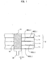
- Fig. 1 shows a part of a cross sectional structure of a sintered substrate made of aluminium nitride with a through-hole 14 as a center(hereinafter referred to as "a ceramic substrate 12"), which is a base substrate of a wafer prober 10.
- the wafer prober 10 is composed of the ceramic substrate 12 having a multiple laminated structure.
- the ceramic substrate 12 is made of alminium nitride material which is provided with the through-hole 14 at an appropriate position, the through-hole 14 being for connection with an external terminal pin.
- the through-hole 14 has projections 16 on its outer circumference of a side wall, from which the projections 16 projects radially into the ceramic substrate 12.
- the through-hole 14 can be of any shape from the side view, such as a cylinder, a plate, a screw, or the like. From the axial view, it can be of any shape such as a circle, a polygon, or the like.
- Reference numerals E1 to E4 denote conductor layers 18 which functions as an electrode E.
- the conductor layers 18 are formed on respective layers L1 to L4 of the ceramic substrate 12 made of aluminium nitride having a laminated structure. Respective conductor layers 18 and the like are connected to the through-hole 14 appropriately.
- respective conductor layers 18 and the like mean a guard electrode E and a ground electrode E formed on respective layers L1 to L4 of the ceramic substrate 12, in addition to this, a general circuit elements, an electric conductor, a resistive body, a semiconductor, such as a heat generation body 34, an electrostatic electrode 36, and the like. Number of lamination are commonly defined as two or more by means of such wiring structure that realizes the electric performance needed for the wafer prober 10.
- the projection 16 which projects into the ceramic substrate 12 encroaches on the ceramic substrate 12 (a bite structure), therefore a contact area between the material filled in the through-hole 14 and the ceramic substrate 12 increases greatly, thus adhesion therebetween is made to be improved. Accordingly, the ceramic substrate 12 has such through-hole structure that has a high reliability and an excellent tolerance against a drawing stress applied to an external terminal pin 20.
- the conductor layer 18 is used as a heat generation body. If the projection 16 is connected to a heat generation body built-in the ceramic substrate 12, then it is not occurred that a heat concentration to the through-hole 14 due to down of a heat conductivity of the ceramic substrate 12, even when a temperature rises above or equal to 200 °C. Accordingly, the specific point (a hot spot) is not formed on a heating surface. Because the projection 16 releases heat, that is formed on a side wall of an outer circumference of the through-hole 14.
- a shape of "the bite structure” changes to some extent due to variation of setting of each process in a method of manufacturing processes described below.
- Each projection 16 may satisfactorily be formed on a boundary between respective layers in the laminated structure on the through-hole 14 having a cylindrical shape or a plate shape, so that its shape of the projection 16 may be of a shape of a brim or a bamboo sheath (see Fig. 2 or Fig. 3).
- the shape of a brim or a bamboo sheath is not necessarily be a continuous shape along an outer circumference of a cylindrical shape or a plate shape.
- a size X (see Fig. 1) of the projection 16 is determined based on the mutual relation with adjacent through-hole 14. The size X is determined within a range of 50 ⁇ m to 0.5 mm in respect with the general through-hole 14 having a diameter within a range of 20 ⁇ m to 10 mm.
- the projection 16 is formed on the lamination boundary between each laminated green sheet body before firing. Because the ceramic substrate 12 is made of a sintered material of a laminated green sheet body. By using general process for molding a green sheet, the number of the projection 16 corresponding to the number of laminated sheets can be formed. Accordingly, the projection 16 can be formed in the ceramic substrate 12 without using a special facilities and/or a complex method.
- a sintered substrate of aluminium nitride is prepared by using above-described sheet forming method.
- Figs. 4 (a) to 4 (c) show processes of forming a punch hole according to one embodiment of the present invention.
- the green sheet 22 employed for the series of processes has such major plane that is adhered to and covered with a base film 24, similar to the conventional sheet.
- a plurality of the green sheets 24 is prepared for the numbers of lamination; a punching hole 26 is formed by punching hole in each green sheet for forming the through-hole 14 (Fig. 2 (b)); the punching hole 26 is filled with conductive material 28; then each green sheet 24 is laminated and sintered.
- a gap 30 is formed at a periphery part 22a around the punching hole 26 by a process of stripping partially the green sheet 22 from the base film 24; then the punching hole 26 is filled with the conductive material 28 for use in a through-hole, and the gap 30 is also filled with the conductive material 28; thereby the projection 16 is formed by the conductive material 28 filled in the gap 30.
- a detail description will be made concerning a method for manufacturing the green sheet on which the above-mentioned gap 30 can be formed.
- a predetermined amount of binder, solvent, sintering agent and the like are added to the powdered aluminium nitride material, in accordance with the predetermined composition; then the obtained mixture is put into a ball mill and the like to mull for a predetermined period of time to prepare a slurry.
- Well-known materials may be used as powdered aluminium nitride and sintering agent.
- the slurry are molded into the green sheets 22 having a predetermined size and shape, in accordance with the method already established for forming shaped-sheets, such as the doctor blade method.
- Method for producing a thin layer of sheets is not limited to the doctor blade method, and it may be a shaping method with a flat-rolling process.
- a doctor blade machine may be used that incorporates a doctor blade, base films and a drying kiln.
- the binder for the green sheets 22 at least one selected from a group consisted of acrylic resin, ethyl cellulose, butylcellosorb and polyvinyl alcohol is preferred.
- the solvent at least one selected from a group consisted of ⁇ -terpineol and glycol is preferred.
- the base material of the base film is polyethylene terephthalate (PET), and the base film is surface-finished so as to be flat, smooth and mold-releasable in order to assure that the green sheets are formed at a constant thickness.
- the green sheet 22 formed on the base film 24 is adhered to the base film, remaining such a degree that the green sheet 22 and the base film 24 can be treated in a body. Once stripping them off, adhesion falls to such a degree it can adhere with difficulty.
- the slurry are once stored in a wet storage in the doctor blade machine; the slurry, shaped in a thin film, are pulled out of the gap between the doctor blade machine and the base film 24 along with the transfer of the base film 24 being taken-up by a winder (not shown). Thickness of the slurry may be adjusted by the gap, thereby a predetermined amount of the slurry are quantitatively rolled out on the base film 24; then the resulting slurry, together with the base film 24, are transferred to the drier kiln. Thickness of the green sheet 22 may be preferably in the range of 0.1 mm to 5 mm.
- the volatile component in solvent contained in the slurry and the like will evaporate and the sheet will be dried and become in a form of a thin film resin, thereby the green sheet 22 on which the base film 24 is formed can be obtained as shown in Fig. 4 (a).
- the green sheet 22 is once taken-up by the winder, remaining that the green sheet 22 being adhered to the base film 24 as it is.
- the punching hole 26 is formed as a cavity at the predetermined position on the green sheet 22 by punching it together with the base film 24 (see Fig. 4 (b)).
- the green sheet 22 is punched by means of a punching machine (not shown) which causes the green sheet 22 to pass through a die with being put between the upper and lower punches; a punching speed is set so that an edge of the base film 24 may be slightly peeled off from an edge of the green sheet 22 to form the gap 30; under the condition, punching process is executed.
- Punching speed may preferably be within a range of 1 m/second to 10 m/second because of easiness of forming the gap 30 and no outbreak of the punching reaction.
- the gap 30 has such structure that the conductive paste is likely to penetrate thereinto.
- an edge of the green sheet 22 on a periphery 22a around the punching hole 26 tends to be shifted from an edge of the base film 24 because of the following reasons: the thermal expansion/shrinkage property of the base film 24 is slightly different from that of the green sheet 22 (the property is depending on the material characteristics), and the dry shrinkage of the green sheet 22 (it shrinks slightly even after being taken out from the drying kiln).
- the predetermined electrodes and the like are printed on the green sheet 22, in accordance with such process as the screen printing process.
- mucilagious conductive paste 28 is employed that contains conductive material being components of the electrode after firing the green sheet 28.
- the conductive material such material that contains the conductive ceramics, the metal particles and the like may be preferable.
- the conductive paste is applied to the green sheet in accordance with the process of the printing method.
- tungsten carbide or molybdenum carbide may be preferable because it is difficult for these materials to oxidize and it is difficult for the thermal conductivity to decline.
- metal particles for example, one selected from a group consisted of tungsten, molybdenum, platinum, nickel, and the like, or more than two selected therefrom may be used.
- Mean particle size of these conductive ceramic particles and these metal particles may be within a range of 0.1 ⁇ m to 10 ⁇ m because of the filling in the through-hole and the printing process. As described below, a range of 1 ⁇ m to 5 ⁇ m may particularly be preferable because of easiness of penetration into a gap.
- Suitable conductive paste is prepared by mixing and uniformly mulling 85 to 97 parts by weight of the conductive component particles or the metal particles, 1.5 to 10 parts by weight of at least one binder selected from a group consisted of acrylic resin, ethyl cellulose, butylcellosorb and polyvinyl alcohol, 1.5 to 10 parts by weight of at least one solvent selected from a group consisted of ⁇ -terpineol, glycol, ethyl alcohol and butanol.
- Viscosity of the conductive paste may preferably be within a range of 50000 to 500000 cps (50 to 500 Pa ⁇ s) because of easiness of penetration into the gap 30 formed at the periphery 22a around the through-hole 14.
- the conductive material 28 in a paste form can penetrate into the gap 30 in a capillary action when being printed on the green sheet 22 in a process of the squeegee method and the roller method.
- a viscosity of a conductive paste can be variable as described above.
- a width of penetration can be controlled by setting a pressure of a squeegee, a roller or the like. With controlling a viscosity of a conductive paste and a pressure of a squeegee or that of a roller or the like, an amount of a conductive paste filled in the through-hole 14 is slightly increased more than that of a prior art, then a conductive paste is caused to penetrate into the gap 30.
- the conductive paste 28 is caused to penetrate into the gap 30, thereby the gap 30 being filled with the conductive paste 28 (Fig. 4 (c)).
- each green sheet 22 is laminated in a correct order so that the predetermined laminated-green sheet body can be obtained; then each green sheet 22 is cut to be a predetermined shape to form a final shape as a molding product before sintering.
- the predetermined electrodes and the like are printed on each green sheet 22.
- the punching position is determined as such a position corresponding to each pattern, and the gap 30 is also formed on the corresponding position similarly.
- the punching hole 26 becomes the through-hole 14 and the conductive material 28 with which the gap 30 is filled becomes the projection 16 which projects from the through-hole 14 like a protrusion.
- the green body may be inserted into a crucible or a setter and the like to decompose and degrease the binder and the like under a temperature of 350 °C to 600 °C for a predetermined period of time. Then the green body will be sintered at approximately 1800 °C for a predetermined period of time.
- the desired sintered-substrate 12 made of aluminium nitride can be obtained, that has the conductive layer 18 (an electrode, a heating body and the like).
- the manufacturing process according to the embodiment of the present invention allows the projection to be formed easily in a process of forming through-hole having the projection because there is no need to use an extra facility and/or a complex method. Although adjustment of punching condition is needed, there is no need to add a new process and/or an expensive parts or the like. Accordingly, cost can go down in the process of manufacturing a wafer prober.
- a hole is punched in the desired position on the green sheet 22 together with the base film 24 so that the through-hole 14 may be formed on the desired position of the green sheet 22 to which the base film 24 is adhered, thereby the punching hole 26 is formed as a cavity.
- a metal mask 32 is placed that has an opening larger than the punching hole 26, then the punching hole 26 is filled with the conductive paste 28.
- One side of the through-hole 14 is shut at the time of filling; then when firing, a circle pattern 28a is printed, that becomes the projective part (the projection 16), on the side face of the through-hole 14.
- Example 1 A wafer prober with a heater
- a ceramic paste composition was made by mixing 100 parts by weight of powdered aluminium nitride (available from Tokuyama Corp., a mean particle diameter 1.1 ⁇ m), 4 parts by weight of yttrium (a mean particle diameter 0.4 ⁇ m), 11.5 parts by weight of acrylic binder, 0.5 parts by weight of dispersant, and 53 parts by weight of alcohol mixture containing 1-butanol and ethanol.
- powdered aluminium nitride available from Tokuyama Corp., a mean particle diameter 1.1 ⁇ m
- yttrium a mean particle diameter 0.4 ⁇ m
- acrylic binder 0.5 parts by weight of dispersant
- 53 parts by weight of alcohol mixture containing 1-butanol and ethanol 53 parts by weight of alcohol mixture containing 1-butanol and ethanol.
- Conductive paste for use in the through-hole was prepared by mixing 100 parts by weight of tungsten carbide having a mean particle diameter of 3 ⁇ m, 1.9 parts by weight of acrylic binder, 3.7 parts by weight of ⁇ -terpineol solvent, and 0.2 parts by weight of dispersant.
- a pattern of the electrodes and the heat generation body are printed and formed on the green sheet by using a method of a prior art. Then the openings for the through-holes and the gap parts were filled with the conductive paste for a through-hole.
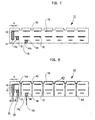
- the through-holes 14 and 14a had a diameter both of 3.0 mm, and a depth of 6.0 mm and 3.0 mm respectively; a size X of a brim of the projection 16 was 100 ⁇ m.
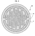
- a surface on the ceramic substrate 12 was provided with a recess for a thermocouple (not shown) and a groove 40 for sucking a silicon wafer.
- titanium, molybdenum and nickel layers were formed on the surface on which the grooves 40 were formed. Furthermore, on the obtained layers, a nickel layer containing a boron content of 1 % by weight or less was caused to deposit by using an electroless nickel plating bath and an electrolytic nickel plating bath; after that it was annealed. Furthermore, a gold plating layer was formed thereon by an electroless gold plating bath to produce a chuck top conductor layer 42 (see Fig. 8).
- Fig. 9 is a picture showing a through-hole of a wafer prober with a heater consistent with Example 1. As shown in Fig. 9, a plurality of projections is formed on the side face of the through-hole.
- the external terminal pin 20 made of Kovar was connected to the blind hole 46 by using a gold flux comprising an Ni-Au alloy (Au of 81.5 % by weight, Ni of 18.4 % by weight, impurity of 0.1 % by weight) by applying reflow under heating at 970 °C.
- the external terminal pin 20 made of Kovar was connected to the heat generation body 34 through a solder layer 48 (see Fig. 8).
- the green sheet was dried at 80 °C for five hours; then the passing through-hole for the through-hole was formed by making an openings by way of drilling, but no gap was produced between PET and the green sheet. On the obtained through-hole, no projection is formed.
- each strength of Examples is higher than that of Comparative example.
- each Example shows a lower value than the Comparative example.
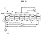
- the wafer prober may be provided with, not only the through-hole 14c for connecting electrically to the chuck top conductive layer, but also the through-holes 14, 14a for connecting electrically to a guard electrode and a ground electrode.
- a side face on the through-hole for connecting to the guard and ground electrodes may be provided with the projection 16 (a portion of a protrusion).
- a recess may be provided for the through-hole.
- the concept of the present invention may be achieved provided that the through-hole is strongly adhered to the ceramic substrate; and that uniformity of whole temperature is achieved.
- the ceramic substrate according to claims 1 to 4 consistent with the present invention allows the through-hole structure to have excellent tolerance against a drawing stress applied to an external terminal pin, and to have excellent reliability performance. Furthermore, it is difficult to cause a hot spot to be formed, thereby achieving uniform distribution of temperatures. According to the present invention, an electrostatic chuck, a wafer prober and a heater that have above-mentioned through hole structure can be manufactured easily. These products achieve high reliability performance against a drawing stress applied to an external terminal pin and further achieve uniform distribution of the temperatures.
Landscapes
- Container, Conveyance, Adherence, Positioning, Of Wafer (AREA)
- Testing Or Measuring Of Semiconductors Or The Like (AREA)
- Surface Heating Bodies (AREA)
Applications Claiming Priority (5)
| Application Number | Priority Date | Filing Date | Title |
|---|---|---|---|
| JP32001099 | 1999-11-10 | ||
| JP32001099 | 1999-11-10 | ||
| JP34969299 | 1999-12-09 | ||
| JP34969299 | 1999-12-09 | ||
| PCT/JP2000/000817 WO2001035459A1 (fr) | 1999-11-10 | 2000-02-15 | Substrat en ceramique |
Publications (1)
| Publication Number | Publication Date |
|---|---|
| EP1124256A1 true EP1124256A1 (fr) | 2001-08-16 |
Family
ID=26569916
Family Applications (1)
| Application Number | Title | Priority Date | Filing Date |
|---|---|---|---|
| EP00902967A Withdrawn EP1124256A1 (fr) | 1999-11-10 | 2000-02-15 | Substrat en ceramique |
Country Status (3)
| Country | Link |
|---|---|
| US (3) | US6632512B1 (fr) |
| EP (1) | EP1124256A1 (fr) |
| WO (1) | WO2001035459A1 (fr) |
Cited By (2)
| Publication number | Priority date | Publication date | Assignee | Title |
|---|---|---|---|---|
| WO2004015770A1 (fr) * | 2002-08-01 | 2004-02-19 | Infineon Technologies Ag | Support de circuit a plusieurs couches et fabrication dudit support |
| FR2850790A1 (fr) * | 2003-02-05 | 2004-08-06 | Semco Engineering Sa | Semelle de collage electrostatique avec electrode radiofrequence et moyens thermostatiques integres |
Families Citing this family (36)
| Publication number | Priority date | Publication date | Assignee | Title |
|---|---|---|---|---|
| EP1120829A4 (fr) * | 1999-08-10 | 2009-05-27 | Ibiden Co Ltd | Plaque ceramique pour dispositif de production de semi-conducteurs |
| EP1249433A4 (fr) * | 1999-09-06 | 2005-01-05 | Ibiden Co Ltd | Briquette et substrat ceramique en nitrure d'aluminium carbone fritte destine a des equipements de fabrication ou de verification de semi-conducteurs |
| US6861165B2 (en) * | 2000-02-24 | 2005-03-01 | Ibiden Co., Ltd. | Aluminum nitride sintered compact, ceramic substrate, ceramic heater and electrostatic chuck |
| JP2001247382A (ja) * | 2000-03-06 | 2001-09-11 | Ibiden Co Ltd | セラミック基板 |
| EP1233651A1 (fr) * | 2000-04-07 | 2002-08-21 | Ibiden Co., Ltd. | Element ceramique chauffant |
| WO2001091166A1 (fr) * | 2000-05-26 | 2001-11-29 | Ibiden Co., Ltd. | Dispositif de fabrication et de controle d'un semi-conducteur |
| JP3516392B2 (ja) * | 2000-06-16 | 2004-04-05 | イビデン株式会社 | 半導体製造・検査装置用ホットプレート |
| EP1229572A1 (fr) * | 2000-07-04 | 2002-08-07 | Ibiden Co., Ltd. | Plaque chaude destinee a la fabrication et aux essais de semiconducteurs |
| US6815646B2 (en) * | 2000-07-25 | 2004-11-09 | Ibiden Co., Ltd. | Ceramic substrate for semiconductor manufacture/inspection apparatus, ceramic heater, electrostatic clampless holder, and substrate for wafer prober |
| JPWO2002084717A1 (ja) * | 2001-04-11 | 2004-08-05 | イビデン株式会社 | 半導体製造・検査装置用セラミックヒータ |
| WO2002101816A1 (fr) * | 2001-06-06 | 2002-12-19 | Ibiden Co., Ltd. | Dispositif d'etalonnage de tranche |
| US20040174954A1 (en) * | 2001-06-28 | 2004-09-09 | Rust Johan Willem | Medical x-ray device and power module therefor |
| KR100511854B1 (ko) * | 2002-06-18 | 2005-09-02 | 아네르바 가부시키가이샤 | 정전 흡착 장치 |
| KR20040008093A (ko) * | 2002-07-17 | 2004-01-28 | 엔지케이 스파크 플러그 캄파니 리미티드 | 동 페이스트 및 그것을 이용한 배선기판 |
| JP3894562B2 (ja) | 2003-10-01 | 2007-03-22 | キヤノン株式会社 | 基板吸着装置、露光装置およびデバイス製造方法 |
| US7057301B1 (en) * | 2004-08-26 | 2006-06-06 | Hewlett-Packard Development Company, L.P. | Semiconductor wafer |
| US20060088692A1 (en) * | 2004-10-22 | 2006-04-27 | Ibiden Co., Ltd. | Ceramic plate for a semiconductor producing/examining device |
| US8226769B2 (en) * | 2006-04-27 | 2012-07-24 | Applied Materials, Inc. | Substrate support with electrostatic chuck having dual temperature zones |
| US7385472B1 (en) * | 2006-06-28 | 2008-06-10 | Emc Corporation | Multi-level printed circuit board interstitial vias |
| JP2008108703A (ja) * | 2006-09-28 | 2008-05-08 | Covalent Materials Corp | 面状ヒータ及びこのヒータを備えた半導体熱処理装置 |
| JP5270310B2 (ja) * | 2008-11-13 | 2013-08-21 | 東京エレクトロン株式会社 | 静電チャック及び基板処理装置 |
| US8405005B2 (en) * | 2009-02-04 | 2013-03-26 | Mattson Technology, Inc. | Electrostatic chuck system and process for radially tuning the temperature profile across the surface of a substrate |
| JP2015008261A (ja) * | 2013-05-28 | 2015-01-15 | 京セラサーキットソリューションズ株式会社 | 配線基板およびその製造方法 |
| KR101483875B1 (ko) * | 2013-07-31 | 2015-01-16 | 삼성전기주식회사 | 글라스 코어기판 및 그 제조방법 |
| US9374910B2 (en) * | 2013-12-31 | 2016-06-21 | International Business Machines Corporation | Printed circuit board copper plane repair |
| US10008404B2 (en) | 2014-10-17 | 2018-06-26 | Applied Materials, Inc. | Electrostatic chuck assembly for high temperature processes |
| US10008399B2 (en) | 2015-05-19 | 2018-06-26 | Applied Materials, Inc. | Electrostatic puck assembly with metal bonded backing plate for high temperature processes |
| US10249526B2 (en) | 2016-03-04 | 2019-04-02 | Applied Materials, Inc. | Substrate support assembly for high temperature processes |
| JP6722518B2 (ja) * | 2016-06-09 | 2020-07-15 | 新光電気工業株式会社 | 焼結体及びその製造方法と静電チャック |
| US11631597B2 (en) | 2017-02-01 | 2023-04-18 | Ngk Spark Plug Co., Ltd. | Holding apparatus |
| US10957572B2 (en) | 2018-05-02 | 2021-03-23 | Applied Materials, Inc. | Multi-zone gasket for substrate support assembly |
| US12238827B2 (en) * | 2019-03-28 | 2025-02-25 | Kyocera Corporation | Base structure and wafer placing device |
| WO2021075241A1 (fr) | 2019-10-18 | 2021-04-22 | 京セラ株式会社 | Structure et dispositif de chauffage |
| JP2022060859A (ja) * | 2020-10-05 | 2022-04-15 | キオクシア株式会社 | 静電チャック装置及び半導体製造装置 |
| JP7569772B2 (ja) * | 2021-10-07 | 2024-10-18 | 日本碍子株式会社 | 半導体製造装置用部材 |
| US20250391699A1 (en) * | 2024-06-20 | 2025-12-25 | Applied Materials Israel Ltd. | Hybrid vacuum electrostatic chuck carrier for high warpage wafers |
Family Cites Families (32)
| Publication number | Priority date | Publication date | Assignee | Title |
|---|---|---|---|---|
| US3346689A (en) * | 1965-01-29 | 1967-10-10 | Philco Ford Corp | Multilayer circuit board suing epoxy cards and silver epoxy connectors |
| US3743421A (en) * | 1971-07-02 | 1973-07-03 | Sperry Rand Corp | System for identifying personnel by fingerprint verification and method therefor |
| US3944978A (en) * | 1974-09-09 | 1976-03-16 | Recognition Systems, Inc. | Electro-optical method and apparatus for making identifications |
| US4336998A (en) * | 1980-05-22 | 1982-06-29 | Siemens Corporation | Fingerprint transducer and reading apparatus |
| US4358677A (en) * | 1980-05-22 | 1982-11-09 | Siemens Corporation | Transducer for fingerprints and apparatus for analyzing fingerprints |
| JPS57182893A (en) | 1981-05-08 | 1982-11-10 | Matsushita Electric Industrial Co Ltd | Digital measuring apparatus |
| JPS57182893U (fr) * | 1981-05-14 | 1982-11-19 | ||
| JPS62130544A (ja) * | 1985-11-30 | 1987-06-12 | Ibiden Co Ltd | 半導体搭載用基板 |
| JPH0697677B2 (ja) * | 1987-04-21 | 1994-11-30 | 東陶機器株式会社 | 静電チャック基盤の製造方法 |
| JPH01145785A (ja) * | 1987-08-21 | 1989-06-07 | Nec Corp | 表面形状計測方法および装置 |
| US5177353A (en) * | 1990-07-31 | 1993-01-05 | Retrievex, Inc. | Finger surface image enhancement having liquid layer on finger touching surface of the plate |
| JPH0812895B2 (ja) * | 1992-11-26 | 1996-02-07 | イビデン株式会社 | 半導体素子搭載ピングリッドアレイパッケージ基板 |
| JP2798570B2 (ja) | 1992-12-01 | 1998-09-17 | 京セラ株式会社 | 静電チャック |
| US5726443A (en) * | 1996-01-18 | 1998-03-10 | Chapman Glenn H | Vision system and proximity detector |
| JPH09213455A (ja) * | 1996-02-05 | 1997-08-15 | Kyocera Corp | ウエハ保持装置の給電構造 |
| FR2754369B1 (fr) * | 1996-10-04 | 1998-12-18 | Thomson Csf | Systeme d'acquisition d'empreintes en relief et procede d'acquisition |
| US6303879B1 (en) * | 1997-04-01 | 2001-10-16 | Applied Materials, Inc. | Laminated ceramic with multilayer electrodes and method of fabrication |
| US6255601B1 (en) * | 1997-04-01 | 2001-07-03 | Applied Materials, Inc. | Conductive feedthrough for a ceramic body and method of fabricating same |
| US6240200B1 (en) * | 1997-08-29 | 2001-05-29 | Barry M. Wendt | Optical fingerprint imager with improved optics |
| US6103978A (en) * | 1997-12-18 | 2000-08-15 | Lucent Technologies Inc. | Printed wiring board having inner test-layer for improved test probing |
| US6000224A (en) * | 1998-03-05 | 1999-12-14 | Foye; Matthew R. | Travel mug |
| DE19818229A1 (de) * | 1998-04-24 | 1999-10-28 | Hauke Rudolf | System zur berührungslosen Hand- und Fingerlinien-Erkennung |
| US6485981B1 (en) * | 1998-07-29 | 2002-11-26 | Ciencia, Inc. | Method and apparatus for imaging and documenting fingerprints |
| US6259108B1 (en) * | 1998-10-09 | 2001-07-10 | Kinetic Sciences Inc. | Fingerprint image optical input apparatus |
| JP2000194829A (ja) * | 1998-12-24 | 2000-07-14 | Mitsubishi Electric Corp | 凹凸パターン読取り装置 |
| US6031729A (en) * | 1999-01-08 | 2000-02-29 | Trw Inc. | Integral heater for reworking MCMS and other semiconductor components |
| WO2000079214A1 (fr) * | 1999-06-23 | 2000-12-28 | Johnson Neldon P | Dispositif et procede de detection d'empreintes digitales |
| JP3228924B2 (ja) | 2000-01-21 | 2001-11-12 | イビデン株式会社 | 半導体製造・検査装置用セラミックヒータ |
| US6643390B1 (en) * | 2000-04-19 | 2003-11-04 | Polaroid Corporation | Compact fingerprint identification device |
| US7272248B2 (en) * | 2001-07-16 | 2007-09-18 | Activcard Ireland Limited | Biometric imaging device compensating for non-biometric parameters |
| US6872916B2 (en) * | 2001-11-13 | 2005-03-29 | Cross Match Technologies, Inc. | System and method for biometric image capturing |
| US6954260B2 (en) * | 2002-01-17 | 2005-10-11 | Cross Match Technologies, Inc. | Systems and methods for illuminating a platen in a print scanner |
-
2000
- 2000-02-15 EP EP00902967A patent/EP1124256A1/fr not_active Withdrawn
- 2000-02-15 WO PCT/JP2000/000817 patent/WO2001035459A1/fr not_active Ceased
- 2000-02-15 US US09/787,954 patent/US6632512B1/en not_active Expired - Lifetime
-
2003
- 2003-01-16 US US10/345,356 patent/US6919124B2/en not_active Expired - Lifetime
-
2004
- 2004-08-16 US US10/918,448 patent/US20050018379A1/en not_active Abandoned
Non-Patent Citations (1)
| Title |
|---|
| See references of WO0135459A1 * |
Cited By (3)
| Publication number | Priority date | Publication date | Assignee | Title |
|---|---|---|---|---|
| WO2004015770A1 (fr) * | 2002-08-01 | 2004-02-19 | Infineon Technologies Ag | Support de circuit a plusieurs couches et fabrication dudit support |
| FR2850790A1 (fr) * | 2003-02-05 | 2004-08-06 | Semco Engineering Sa | Semelle de collage electrostatique avec electrode radiofrequence et moyens thermostatiques integres |
| WO2004070829A1 (fr) * | 2003-02-05 | 2004-08-19 | Semco Engineering S.A | Semelle de collage electrostatique avec electrode radiofrequence et moyens thermostatiques integres |
Also Published As
| Publication number | Publication date |
|---|---|
| WO2001035459A1 (fr) | 2001-05-17 |
| US20030104186A1 (en) | 2003-06-05 |
| US6919124B2 (en) | 2005-07-19 |
| US6632512B1 (en) | 2003-10-14 |
| US20050018379A1 (en) | 2005-01-27 |
Similar Documents
| Publication | Publication Date | Title |
|---|---|---|
| US6919124B2 (en) | Ceramic substrate | |
| EP1881519B1 (fr) | Chauffage pour mandrin électrostatique | |
| WO2001039551A1 (fr) | Plaque chauffante en ceramique | |
| EP1286390A1 (fr) | Substrat ceramique pour dispositif de fabrication de semi-conducteurs | |
| KR20020092967A (ko) | 세라믹 기판 및 그 제조 방법 | |
| WO2001013423A1 (fr) | Plaque ceramique pour dispositif de production de semi-conducteurs | |
| CN106007683A (zh) | 氧化铝烧结体的制法以及氧化铝烧结体 | |
| KR20010090740A (ko) | 세라믹 히터 | |
| WO2001078455A1 (fr) | Plaque ceramique | |
| JP2003204156A (ja) | セラミック基板 | |
| CN115152322B (zh) | 陶瓷加热器及其制法 | |
| JP2001230306A (ja) | セラミック基板 | |
| JP2001287982A (ja) | サセプタ及びその製造方法 | |
| JP3222119B2 (ja) | 半導体製造・検査装置用セラミックヒータ | |
| JP2001319967A (ja) | セラミック基板の製造方法 | |
| CN114390733B (zh) | 陶瓷加热器 | |
| JP2001223257A (ja) | 半導体製造・検査装置用セラミック基板 | |
| JP2002173378A (ja) | 半導体処理装置用セラミックス部材の製造方法 | |
| JP3584203B2 (ja) | 半導体製造・検査装置用セラミック基板 | |
| JP2001332560A (ja) | 半導体製造・検査装置 | |
| JP2005116608A (ja) | プラズマ発生装置用電極埋設部材 | |
| JP2004356638A (ja) | 半導体製造・検査装置用セラミック基板 | |
| JP2002124446A (ja) | 半導体製造・検査装置用セラミックヒータ | |
| JP2000243818A (ja) | 静電チャックの製造方法 | |
| JP2001308163A (ja) | 半導体製造・検査装置用セラミック基板 |
Legal Events
| Date | Code | Title | Description |
|---|---|---|---|
| PUAI | Public reference made under article 153(3) epc to a published international application that has entered the european phase |
Free format text: ORIGINAL CODE: 0009012 |
|
| AK | Designated contracting states |
Kind code of ref document: A1 Designated state(s): AT BE CH CY DE DK ES FI FR GB GR IE IT LI LU MC NL PT SE |
|
| 17P | Request for examination filed |
Effective date: 20010824 |
|
| STAA | Information on the status of an ep patent application or granted ep patent |
Free format text: STATUS: THE APPLICATION HAS BEEN WITHDRAWN |
|
| 18W | Application withdrawn |
Effective date: 20050404 |