EP1126566B1 - Structure de guide d'ondes optique - Google Patents
Structure de guide d'ondes optique Download PDFInfo
- Publication number
- EP1126566B1 EP1126566B1 EP01301274A EP01301274A EP1126566B1 EP 1126566 B1 EP1126566 B1 EP 1126566B1 EP 01301274 A EP01301274 A EP 01301274A EP 01301274 A EP01301274 A EP 01301274A EP 1126566 B1 EP1126566 B1 EP 1126566B1
- Authority
- EP
- European Patent Office
- Prior art keywords
- waveguide
- pump
- region
- site
- article
- Prior art date
- Legal status (The legal status is an assumption and is not a legal conclusion. Google has not performed a legal analysis and makes no representation as to the accuracy of the status listed.)
- Expired - Lifetime
Links
Images


Classifications
-
- H—ELECTRICITY
- H01—ELECTRIC ELEMENTS
- H01S—DEVICES USING THE PROCESS OF LIGHT AMPLIFICATION BY STIMULATED EMISSION OF RADIATION [LASER] TO AMPLIFY OR GENERATE LIGHT; DEVICES USING STIMULATED EMISSION OF ELECTROMAGNETIC RADIATION IN WAVE RANGES OTHER THAN OPTICAL
- H01S3/00—Lasers, i.e. devices using stimulated emission of electromagnetic radiation in the infrared, visible or ultraviolet wave range
- H01S3/05—Construction or shape of optical resonators; Accommodation of active medium therein; Shape of active medium
- H01S3/06—Construction or shape of active medium
- H01S3/063—Waveguide lasers, i.e. whereby the dimensions of the waveguide are of the order of the light wavelength
- H01S3/0632—Thin film lasers in which light propagates in the plane of the thin film
-
- G—PHYSICS
- G02—OPTICS
- G02F—OPTICAL DEVICES OR ARRANGEMENTS FOR THE CONTROL OF LIGHT BY MODIFICATION OF THE OPTICAL PROPERTIES OF THE MEDIA OF THE ELEMENTS INVOLVED THEREIN; NON-LINEAR OPTICS; FREQUENCY-CHANGING OF LIGHT; OPTICAL LOGIC ELEMENTS; OPTICAL ANALOGUE/DIGITAL CONVERTERS
- G02F1/00—Devices or arrangements for the control of the intensity, colour, phase, polarisation or direction of light arriving from an independent light source, e.g. switching, gating or modulating; Non-linear optics
- G02F1/35—Non-linear optics
- G02F1/365—Non-linear optics in an optical waveguide structure
-
- H—ELECTRICITY
- H01—ELECTRIC ELEMENTS
- H01S—DEVICES USING THE PROCESS OF LIGHT AMPLIFICATION BY STIMULATED EMISSION OF RADIATION [LASER] TO AMPLIFY OR GENERATE LIGHT; DEVICES USING STIMULATED EMISSION OF ELECTROMAGNETIC RADIATION IN WAVE RANGES OTHER THAN OPTICAL
- H01S3/00—Lasers, i.e. devices using stimulated emission of electromagnetic radiation in the infrared, visible or ultraviolet wave range
- H01S3/05—Construction or shape of optical resonators; Accommodation of active medium therein; Shape of active medium
- H01S3/06—Construction or shape of active medium
- H01S3/063—Waveguide lasers, i.e. whereby the dimensions of the waveguide are of the order of the light wavelength
- H01S3/067—Fibre lasers
- H01S3/06708—Constructional details of the fibre, e.g. compositions, cross-section, shape or tapering
- H01S3/06745—Tapering of the fibre, core or active region
-
- H—ELECTRICITY
- H01—ELECTRIC ELEMENTS
- H01S—DEVICES USING THE PROCESS OF LIGHT AMPLIFICATION BY STIMULATED EMISSION OF RADIATION [LASER] TO AMPLIFY OR GENERATE LIGHT; DEVICES USING STIMULATED EMISSION OF ELECTROMAGNETIC RADIATION IN WAVE RANGES OTHER THAN OPTICAL
- H01S3/00—Lasers, i.e. devices using stimulated emission of electromagnetic radiation in the infrared, visible or ultraviolet wave range
- H01S3/09—Processes or apparatus for excitation, e.g. pumping
- H01S3/091—Processes or apparatus for excitation, e.g. pumping using optical pumping
- H01S3/094—Processes or apparatus for excitation, e.g. pumping using optical pumping by coherent light
- H01S3/094003—Processes or apparatus for excitation, e.g. pumping using optical pumping by coherent light the pumped medium being a fibre
Definitions
- the present invention relates to a waveguide structure for use with a pump laser that is designed to counteract pump depletion.
- the waveguide structure may comprise an erbium-doped waveguide amplifier, a nonlinear waveguide wavelength converter device, or an optical fiber, and is particularly useful in communications systems and wavelength conversion applications.
- Optical communications systems are useful for transmitting optical signals over long distances at high speeds.
- An optical signal which comprises a series of light pulses, is transmitted from a light source, e . g ., a laser, to a waveguide and ultimately to a detector.
- Optical communications systems typically include a variety of devices (e . g ., light sources, photodetectors, switches, optical fibers, amplifiers, filters, and so forth). Amplifiers and filters may be used to propagate the light pulses along the length of the waveguide from the light source to the detector.
- Recently, demand has been increasing for the efficient, large-scale manufacturing of hybrid integrated opto-electronic devices. There is particular interest in the integration of multiple components onto a single chip and hybridization of various components into a single package.
- an optical waveguide structure comprises an inner or core region fabricated from a material having a certain index of refraction, and an outer region contiguous the core comprised of a material having a lower index of refraction than the core. As long as the refractive index of the core exceeds that of the outer region, a light beam propagated along the core will be guided along the length of the waveguide.
- Planar waveguides are flat structures that guide light in essentially the same way as optical fibers.
- a planar waveguide structure comprises a strip of material embedded in a substrate where the waveguide strip has a relatively high index of refraction relative to the substrate.
- One or more amplifying systems may be disposed along the waveguide transmission path for amplifying the transmitted signal.
- EP-A-0454865 and JP 03 005733 each describe waveguide structures comprising a rare earth doped waveguide region and a second undoped region having a lower index of refraction for guiding transmission light and pump light.
- the effective area of the waveguide region at a first pump site is larger than at a second pump site for reducing the decrease in pump power density along the waveguide.
- FIG. 1 schematically shows an amplifier utilizing an optical fiber 11.
- a weak optical signal I s enters from the left, passes through an optical isolator 12 and a filter 13 that blocks pump light and transmits the signal wavelength.
- the light enters a doped fiber 11, typically a rare-earth doped fiber.
- the amplifier is then illuminated with light from the pump laser 15 which introduces a pump signal P s to the fiber to excite the dopant atoms, raise them to a higher energy level, and amplify the weak input signal I s to amplified signal A s transmitted through the waveguide.
- a coupler 16 at the end of the amplifier routes the amplified signal to the output fiber, separating it from the pump light, to produce output signal O s .
- the pump laser 15 is shown at the distal end of the waveguide amplifier adjacent the output, light can be pumped into the amplifier adjacent the input, following the direction of the amplified signal A s .
- the pump laser field gets absorbed as a function of propagation distance in a linear or nonlinear fashion. This absorption produces pump-depletion as a function of propagation distance. The depletion in turn implies a lower efficiency for the amplification or conversion process due to a reduction in pump power density in the waveguide at distances from the pump laser.
- the invention embraces an article including a waveguide structure for use with a pump light source, e.g. , a pump laser, that preserves pump power density.
- the waveguide structure comprises a waveguide region having a first index of refraction, and a second region having a second index of refraction contiguous the waveguide region, wherein the second index of refraction is lower than the first index of refraction so that light launched into the waveguide structure is guided within the waveguide region.
- the waveguide region has a pump propagation length which is defined as a select distance between a first pump site and a second pump site and over which pump light is transmitted within the waveguide region for signal amplification or conversion.
- the effective area of the waveguide region is substantially larger at the first pump site than at the second pump site and thus, the waveguide region is tapered over the pump propagation length, thereby reducing the depletion of pump power density.
- the first pump site is located along the length of the waveguide region at a predetermined distance from the transmission input site.
- the waveguide structure may comprise a planar waveguide or an optical fiber.
- a waveguide structure that counteracts the reduction in pump power density.
- the waveguide structure is adapted for use in a system comprising a pump source and a signal source for simultaneously launching pump and transmission optical fields, respectively, into the waveguide structure; a coupler for combining the pump and the transmission optical fields; and one or more filters, amplifiers, receivers, spectrum analyzers, or other optical components.
- transmission optical field is used herein to distinguish the light transmitted in the waveguide structure from the pump (laser field) used for amplification or conversion.
- the waveguide structure has a waveguide region along which the pump and transmission optical fields are guided.
- the waveguide region has a pump propagation length defined as a select distance between a first pump site and a second pump site over which pump light is transmitted within the waveguide region for signal amplification or conversion.
- the effective area, e . g ., width, of the waveguide region is substantially larger at the first pump site than at the second pump site and thus, the waveguide region is tapered over the pump propagation length, thereby counteracting the depletion of pump light.
- the first and second pump sites can be located at various points along the length of the waveguide while still carrying out the inventive concepts.
- the first pump site is distal the transmission input site, with the second pump site being closer to the transmission input site than the first pump site.
- many alternative embodiments are contemplated, with the important consideration being that the effective area of the waveguide region is reduced, e.g., a taper is introduced, over a length of the waveguide for which pump fields are propagated for amplification or conversion. Due to this taper, the decrease in pump power density is reduced as compared with prior art systems, and preferably is kept substantially constant over the pump propagation length, thereby counteracting pump depletion, due to absorption and losses.
- FIG. 2 schematically illustrates a waveguide structure 20 comprising a waveguide region 21 and a contiguous or second region 22.
- the waveguide structure comprises a planar waveguide deposited on a substrate 10, such that the waveguide region 21 is not completely surrounded by the second region 22, but also is exposed to air at the top of the structure. Air has a lower refractive index (n i ⁇ 1.0) than the waveguide region (typically ⁇ 1.46).
- the waveguide structure has a pump propagation length (L pp ) defined as a select distance between a first pump site 24 and a second pump site 26 over which pump light is transmitted within the waveguide region for amplification or conversion.
- the effective area e.g.
- width, of the waveguide region is substantially larger at the first pump site 24 than at the second pump site 26 and consequently, the waveguide region is tapered over the pump propagation length.
- the pump light will be introduced into the waveguide region from the pump source at the first pump site, as this site is located at the edge of the waveguide structure.
- the transmission optical field may be introduced into the waveguide structure at either the first or second pump sites 24, 26.
- FIG. 2 shows a planar waveguide, these same concepts can be applied to an optical fiber used as a waveguide, e.g. , as illustrated in FIG. 1, where the core of the fiber comprises the waveguide region 21 and a cladding surrounds the core to define the contiguous second region 22.
- the pump power is maintained constant over a given length of the waveguide region, i.e., there is no decay in pump brightness.
- Dp p(z)/A eff
- D p the pump density
- p( z ) the pump power at a given distance ( z ) along the waveguide
- z is a given distance at which the pump light has traveled within the waveguide region
- a eff is the effective area of the mode.
- D p is preferably kept constant, but the pump power is a function of propagation distance and will decrease with increases in z .
- the value for A eff should decrease with decreases in the pump power p( z ) and preferably be as small as possible.
- light may leak from the waveguide, depleting the pump or transmission optical fields, and eventually the waveguide could stop guiding light.
- an adiabatic taper is used, i . e ., one that is sufficiently gradual that the mode is maintained over the waveguide region and scattering losses are negligible.
- An adiabatic taper may be achieved when the waveguide region is tapered by a few microns for a waveguide length of approximately 1 cm, or more preferably, for a length of a few micron or less.
- a waveguide having a width at the first pump site of about 10-30 ⁇ m may be reduced to a width that is as small as possible while still allowing for the transmission of light, e . g ., down to ⁇ 1-3 ⁇ m.
- the width of the waveguide at the first pump site may be within a range of from 2-15 ⁇ m and then narrowed down to a smaller width in the range of about 1-3 ⁇ m.
- the degree of taper preferred for achieving the largest reduction in pump power depletion with smallest losses would depend upon the materials used, the concentration and type of dopants, the length of the waveguide region and pump propagation length, the width of the waveguide region at the first and second pump sites, the pump power, and other factors.
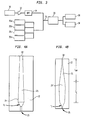
- FIG. 3 illustrates a schematic diagram of a difference frequency generation (DFG) wavelength converter system in which the waveguide structure may be used.
- DFG difference frequency generation
- a pump laser 30 is an external cavity laser for emitting signals amplified by an erbium-doped fiber amplifier 32, e.g. , to a level of ⁇ 300 mW, filtered through a bandpass filter 34, and launched into the transmission path 31.
- the pump light is thus combined with transmission optical fields generated by four different external cavity lasers 35a, 35b, 35c, 35d, and the pump and transmission fields are launched into the waveguide structure 20.
- the output from the waveguide structure may be fiber coupled and analyzed in an optical spectrum analyzer 36 and power meter 38.
- a simultaneous multi-channel wavelength conversion may be performed with pump power launched into the waveguide.
- the efficiency of the conversion process would be limited by pump depletion. While the conversion efficiency could be improved with higher pump powers and different operating conditions ( e . g ., use of higher temperatures, or a different selection of dopants or quasi-phase matching grating periods), pump depletion places inherent limits on the process efficiency.
- Use of the tapered waveguide improves the efficiency which in turn, enhances the flexibility of the system configuration, e . g ., the same or greater efficiencies can be achieved while using lower pump powers and/or with fewer constraints on the system design.
- FIGS. 4A and 4B illustrate alternative embodiments of the waveguide structure, i . e ., reflecting top plan views of planar waveguide structures comprising an inner waveguide region 21 and a contiguous or second region 22.
- an optional initial outward taper T i at the input of the waveguide i.e., where the pump and transmission optical fields are introduced into the waveguide.
- This initial outward taper T i is advantageous for amplifier applications.
- the first pump site is not shown at the waveguide edge or input 25, but at a point 24' inward of waveguide edge at the end of the initial outward taper.
- the waveguide diameter is initially tapered outward for amplification over the initial tapered region T i , the waveguide diameter is then maintained substantially constant over a certain intermediate waveguide distance I c , and then the waveguide diameter is tapered inward over a section of the waveguide defined herein as the pump propagation length between the first pump site 24' and the second pump site 26.'
- the taper can be optimized depending on the application and optical process. For example, applying the embodiments of FIGS. 4A-4B, in operation both pump and transmission optical fields may be launched together into a single mode region of the waveguide. Then this region may be tapered to the intermediate (or wide gain) region where a different concentration of erbium dopants are introduced.
- the wide gain region may comprise a single mode or a multimode waveguide.
- the taper at both ends of the fiber advantageously comprises an adiabatic taper, i . e ., by "adiabatic" it is meant that the degree of the taper is sufficiently gradual that scattering losses are negligible and the lowest mode of the waveguide is constantly used for transmission.
- the wide region is important in an amplifier application so that there are sufficient Er atoms to provide optical gain. Because of the adiabatic transition, both pump and signal beams excite the lowest mode of the wide gain region of the waveguide. As the pump beams travel along the waveguide, their power is reduced due to absorption caused by the Er atoms. The absorption ordinarily would lead to an exponential decay of the pump power as a function of the waveguide length. However, the taper introduced at the end of the wide gain region, e . g ., at the first pump site 24', counteracts the exponential decay. Again, in the case of the multimode waveguide, the taper advantageously has an adiabatic transition, i . e ., the taper can be designed as an exponential taper which is narrow towards the end, as in FIG. 4B, so that the pump power density is kept substantially constant through the length of the multimode region. The taper can be in two or three dimensions.
- FIG. 5A reflects a pump density profile as a function of propagation distance for an untapered, straight 5 ⁇ m wide Er-doped waveguide having a length of 1 cm; and FIG. 5B reflects the pump density profile for the same waveguide where a taper is introduced.
- the wavelength was 980 nm
- the core index of refraction is 1.6
- the second index of refraction is 1.45.
- the pump density profile shows how the absorption in the waveguide depletes the field of the propagating light. If this light is used to pump erbium atoms for gain, it will result in lower gain towards the end of the waveguide.
- FIG. 5A reflects a pump density profile as a function of propagation distance for an untapered, straight 5 ⁇ m wide Er-doped waveguide having a length of 1 cm
- the wavelength was 980 nm
- the core index of refraction is 1.6
- the second index of refraction is 1.45.
- the pump density profile shows how the ab
- FIG. 5B a taper has been introduced, wherein the width of the waveguide is decreased linearly from 5 ⁇ m to 2.5 ⁇ m.
- the pump brightness decay has been substantially reduced as compared with FIG. 5A.
- the profile of FIG. 5B reflects a loss of about 3.5 dB/cm, or a loss of less than 25% of the original pump power.
- the profile of FIG. 5A reflects a loss of more than 50% of the pump power. Any degree of improvement in brightness decay is advantageous.
Landscapes
- Physics & Mathematics (AREA)
- Electromagnetism (AREA)
- Engineering & Computer Science (AREA)
- Plasma & Fusion (AREA)
- Optics & Photonics (AREA)
- Lasers (AREA)
- Optical Integrated Circuits (AREA)
Claims (8)
- Article comportant une structure de guide d'ondes destiné à être utilisé avec une première source pour introduire des champs optiques de transmission dans la structure de guide d'ondes au niveau du site d'entrée de transmission et une seconde source pour émettre une lumière de pompage pour une amplification ou conversion, la structure de guide d'ondes comprenant :une région de guide d'ondes ayant un premier indice de réfraction ;une seconde région ayant un second indice de réfraction contiguë à la région de guide d'ondes, le second indice de réfraction étant inférieur au premier indice de réfraction si bien qu'un champ optique de transmission lancé dans la structure de guide d'ondes depuis la première source est guidé dans la région de guide d'ondes et la lumière de pompage lancée dans la structure de guide d'ondes amplifie ou convertit le champ optique de transmission ;dans lequel la région de guide d'ondes a un premier site de pompage et un second site de pompage entre lesquels la lumière de pompage est transmise dans la région de guide d'ondes pour une amplification ou conversion afin de définir une longueur de propagation de pompage Lpp, et l'aire efficace de la région de guide d'ondes est supérieure au niveau du premier site de pompage par rapport au deuxième site de pompage pour réduire la diminution de la densité de puissance de pompage le long du guide d'ondes ;caractérisé en ce que :le premier site de pompage est situé le long de la longueur de la région de guide d'ondes à une distance prédéterminée du site de transmission d'entrée.
- Article selon la revendication 1, dans lequel la région de guide d'ondes est adiabatiquement effilée sur la longueur de propagation de pompage.
- Article selon la revendication 1, dans lequel la région de guide d'ondes a une première largeur au niveau du site d'entrée de transmission et une deuxième largeur située à une position le long de la région de guide d'ondes, la deuxième largeur étant supérieure à la première largeur afin de définir une région effilée initiale.
- Article selon la revendication 3, dans lequel le premier site de pompage est placé à une extrémité de la région effilée initiale distale du site d'entrée de transmission.
- Article selon la revendication 1, dans lequel la structure de guide d'ondes comprend un guide d'ondes planaire.
- Article selon la revendication 1, dans lequel la structure de guide d'ondes comprend une fibre optique.
- Article selon la revendication 1, comprenant un amplificateur de guide d'ondes.
- Article selon la revendication 1, comprenant un dispositif de conversion de longueurs d'ondes à guide d'ondes.
Applications Claiming Priority (2)
| Application Number | Priority Date | Filing Date | Title |
|---|---|---|---|
| US09/503,378 US6411757B1 (en) | 2000-02-14 | 2000-02-14 | Article comprising a waveguide structure with improved pump utilization |
| US503378 | 2000-02-14 |
Publications (3)
| Publication Number | Publication Date |
|---|---|
| EP1126566A2 EP1126566A2 (fr) | 2001-08-22 |
| EP1126566A3 EP1126566A3 (fr) | 2003-01-15 |
| EP1126566B1 true EP1126566B1 (fr) | 2006-08-02 |
Family
ID=24001834
Family Applications (1)
| Application Number | Title | Priority Date | Filing Date |
|---|---|---|---|
| EP01301274A Expired - Lifetime EP1126566B1 (fr) | 2000-02-14 | 2001-02-13 | Structure de guide d'ondes optique |
Country Status (4)
| Country | Link |
|---|---|
| US (1) | US6411757B1 (fr) |
| EP (1) | EP1126566B1 (fr) |
| JP (1) | JP4812175B2 (fr) |
| DE (1) | DE60121842T2 (fr) |
Families Citing this family (13)
| Publication number | Priority date | Publication date | Assignee | Title |
|---|---|---|---|---|
| GB9928696D0 (en) * | 1999-12-03 | 2000-02-02 | Swan Thomas & Co Ltd | Optical devices and methods of manufacture thereof |
| CA2404451A1 (fr) * | 2000-02-25 | 2001-08-30 | Princeton Lightwave, Inc. | Diode superluminescente haute puissance a guide d'onde courbe multipasse |
| JP2004055717A (ja) * | 2002-07-18 | 2004-02-19 | Oki Electric Ind Co Ltd | 可変光利得制御器 |
| US6970624B2 (en) * | 2003-06-13 | 2005-11-29 | Furukawa Electric North America | Cladding pumped optical fiber gain devices |
| EP1961084A1 (fr) * | 2005-12-09 | 2008-08-27 | Philips Intellectual Property & Standards GmbH | Laser a guide d'ondes a pompage optique dote d'un tronçon de guide d'ondes de transition |
| JP2009059924A (ja) * | 2007-08-31 | 2009-03-19 | Sunx Ltd | レーザ発生装置及びレーザ加工装置 |
| US8229265B2 (en) * | 2007-11-21 | 2012-07-24 | Adc Telecommunications, Inc. | Fiber distribution hub with multiple configurations |
| CN104205533B (zh) | 2012-03-26 | 2018-03-30 | 英特尔公司 | 包括抗谐振波导的混合激光器 |
| US9122003B2 (en) * | 2012-07-18 | 2015-09-01 | Sumitomo Electric Industries, Ltd. | Semiconductor optical device |
| CN105474481B (zh) | 2013-09-16 | 2019-11-05 | 英特尔公司 | 包括光波导的混合式光学装置 |
| US10025033B2 (en) | 2016-03-01 | 2018-07-17 | Advanced Semiconductor Engineering, Inc. | Optical fiber structure, optical communication apparatus and manufacturing process for manufacturing the same |
| US10241264B2 (en) | 2016-07-01 | 2019-03-26 | Advanced Semiconductor Engineering, Inc. | Semiconductor device packages |
| KR102826086B1 (ko) * | 2023-02-10 | 2025-06-27 | 한국과학기술원 | 다중 분산파의 초연속체 생성 장치 및 이를 위한 도파로 구조 설계 방법 |
Family Cites Families (14)
| Publication number | Priority date | Publication date | Assignee | Title |
|---|---|---|---|---|
| JPH035733A (ja) * | 1989-06-01 | 1991-01-11 | Seiko Epson Corp | 光二次高調波発生素子 |
| EP0454865B1 (fr) * | 1989-11-20 | 1996-05-01 | Fujitsu Limited | Amplificateur optique |
| DK285490D0 (da) * | 1990-11-30 | 1990-11-30 | Nordiske Kabel Traad | Fremgangsmaade og apparat til forstaerkning af et optisk signal |
| IT1245019B (it) * | 1991-01-30 | 1994-09-13 | Cselt Centro Studi Lab Telecom | Sistema di pompaggio di laser o amplifiatori a guida d'onda |
| JP2545719B2 (ja) * | 1991-03-15 | 1996-10-23 | 東京工業大学長 | 積層型光増幅器 |
| US5539571A (en) * | 1992-09-21 | 1996-07-23 | Sdl, Inc. | Differentially pumped optical amplifer and mopa device |
| US5392308A (en) * | 1993-01-07 | 1995-02-21 | Sdl, Inc. | Semiconductor laser with integral spatial mode filter |
| GB9305604D0 (en) * | 1993-03-18 | 1993-05-05 | British Telecomm | Optical amplifier and laser |
| JP3588195B2 (ja) * | 1996-07-18 | 2004-11-10 | 浜松ホトニクス株式会社 | 固体レーザ増幅器 |
| EP0867985B1 (fr) * | 1997-03-27 | 2001-02-14 | Nederlandse Organisatie Voor Toegepast-Natuurwetenschappelijk Onderzoek Tno | Guide d'onde planaire dopée à l'erbium |
| US5861981A (en) * | 1997-08-20 | 1999-01-19 | Ditech Corporation | Optical amplifier having dynamically shaped gain |
| US6014396A (en) * | 1997-09-05 | 2000-01-11 | Sdl, Inc. | Flared semiconductor optoelectronic device |
| JP3266194B2 (ja) * | 1999-02-18 | 2002-03-18 | 日本電気株式会社 | 光導波路並びにその光導波路を用いたレーザ発振器およびレーザ増幅器 |
| US6324326B1 (en) * | 1999-08-20 | 2001-11-27 | Corning Incorporated | Tapered fiber laser |
-
2000
- 2000-02-14 US US09/503,378 patent/US6411757B1/en not_active Expired - Lifetime
-
2001
- 2001-02-13 EP EP01301274A patent/EP1126566B1/fr not_active Expired - Lifetime
- 2001-02-13 DE DE60121842T patent/DE60121842T2/de not_active Expired - Lifetime
- 2001-02-13 JP JP2001035271A patent/JP4812175B2/ja not_active Expired - Fee Related
Also Published As
| Publication number | Publication date |
|---|---|
| DE60121842T2 (de) | 2007-01-11 |
| JP2001267664A (ja) | 2001-09-28 |
| DE60121842D1 (de) | 2006-09-14 |
| EP1126566A2 (fr) | 2001-08-22 |
| EP1126566A3 (fr) | 2003-01-15 |
| US6411757B1 (en) | 2002-06-25 |
| JP4812175B2 (ja) | 2011-11-09 |
Similar Documents
| Publication | Publication Date | Title |
|---|---|---|
| US5708669A (en) | Article comprising a cladding-pumped optical fiber laser | |
| Kitagawa et al. | Guided-wave laser based on erbium-doped silica planar lightwave circuit | |
| EP0527265B1 (fr) | Amplificateur à fibre optique ayant un spectre de gain modifié | |
| CA2057480C (fr) | Amplificateur a fibre optique avec filtre | |
| US7489439B2 (en) | Semiconductor Raman ring amplifier | |
| US6411757B1 (en) | Article comprising a waveguide structure with improved pump utilization | |
| EP1456918A1 (fr) | Amplification raman a fibre microdimensionnee | |
| EP0454865B1 (fr) | Amplificateur optique | |
| JP2008511862A (ja) | 半導体に基づくラマンレーザ及び増幅器用半導体導波路における二光子吸収による生成キャリアのライフタイム短縮 | |
| CA2276997C (fr) | Fibre optique pour un amplificateur optique et amplificateur de fibre optique | |
| US5128801A (en) | Integrated optical signal amplifier | |
| JP2004250251A (ja) | 蛍光性ガラス、光増幅用導波路および光増幅モジュール | |
| US20020191926A1 (en) | High gain rare earth doped phosphate glass optical amplification fibers | |
| EP1648055A1 (fr) | Fibre optique et amplificateur à fibre optique hybride l'utilisant | |
| CA2035408C (fr) | Amplificateur de signaux optique a guide de lumiere integre | |
| US20070127877A1 (en) | Amplifying optical fiber | |
| US6173096B1 (en) | Switching temporal optical solitons in a planar lightguide circuit | |
| US5805332A (en) | Optical fiber amplifier | |
| KR100668289B1 (ko) | 광섬유 | |
| Nakazawa et al. | An ultra-efficient erbium-doped fiber amplifier of 10.2 dB/mW at 0.98 μm pumping and 5.1 dB/mW at 1.48 μm pumping | |
| US6259848B1 (en) | Propagating temporal optical solitons in a planar lightguide circuit | |
| JP2842481B2 (ja) | 光増幅器 | |
| KR100460203B1 (ko) | 클래딩 여기 광섬유 증폭기에서의 장주기 광섬유 격자를 이용한 신호 광 증폭 방법 | |
| Kondo et al. | Broadband amplification of Er-doped bismuthate waveguide with> 10 dBm output powers from 1527 to 1573 nm | |
| Kondo et al. | 1-cm2-size Er-doped waveguide based on bismuthate glass for compact amplifier with> 15 dB gain at whole C-band |
Legal Events
| Date | Code | Title | Description |
|---|---|---|---|
| PUAI | Public reference made under article 153(3) epc to a published international application that has entered the european phase |
Free format text: ORIGINAL CODE: 0009012 |
|
| AK | Designated contracting states |
Kind code of ref document: A2 Designated state(s): AT BE CH CY DE DK ES FI FR GB GR IE IT LI LU MC NL PT SE TR |
|
| AX | Request for extension of the european patent |
Free format text: AL;LT;LV;MK;RO;SI |
|
| PUAL | Search report despatched |
Free format text: ORIGINAL CODE: 0009013 |
|
| AK | Designated contracting states |
Kind code of ref document: A3 Designated state(s): AT BE CH CY DE DK ES FI FR GB GR IE IT LI LU MC NL PT SE TR |
|
| AX | Request for extension of the european patent |
Free format text: AL;LT;LV;MK;RO;SI |
|
| 17P | Request for examination filed |
Effective date: 20030318 |
|
| AKX | Designation fees paid |
Designated state(s): DE FR GB |
|
| 17Q | First examination report despatched |
Effective date: 20041125 |
|
| GRAP | Despatch of communication of intention to grant a patent |
Free format text: ORIGINAL CODE: EPIDOSNIGR1 |
|
| GRAS | Grant fee paid |
Free format text: ORIGINAL CODE: EPIDOSNIGR3 |
|
| GRAA | (expected) grant |
Free format text: ORIGINAL CODE: 0009210 |
|
| AK | Designated contracting states |
Kind code of ref document: B1 Designated state(s): DE FR GB |
|
| REG | Reference to a national code |
Ref country code: GB Ref legal event code: FG4D |
|
| REF | Corresponds to: |
Ref document number: 60121842 Country of ref document: DE Date of ref document: 20060914 Kind code of ref document: P |
|
| ET | Fr: translation filed | ||
| PLBE | No opposition filed within time limit |
Free format text: ORIGINAL CODE: 0009261 |
|
| STAA | Information on the status of an ep patent application or granted ep patent |
Free format text: STATUS: NO OPPOSITION FILED WITHIN TIME LIMIT |
|
| 26N | No opposition filed |
Effective date: 20070503 |
|
| PGFP | Annual fee paid to national office [announced via postgrant information from national office to epo] |
Ref country code: FR Payment date: 20140211 Year of fee payment: 14 |
|
| PGFP | Annual fee paid to national office [announced via postgrant information from national office to epo] |
Ref country code: GB Payment date: 20140212 Year of fee payment: 14 |
|
| PGFP | Annual fee paid to national office [announced via postgrant information from national office to epo] |
Ref country code: DE Payment date: 20140417 Year of fee payment: 14 |
|
| REG | Reference to a national code |
Ref country code: DE Ref legal event code: R119 Ref document number: 60121842 Country of ref document: DE |
|
| GBPC | Gb: european patent ceased through non-payment of renewal fee |
Effective date: 20150213 |
|
| REG | Reference to a national code |
Ref country code: FR Ref legal event code: ST Effective date: 20151030 |
|
| PG25 | Lapsed in a contracting state [announced via postgrant information from national office to epo] |
Ref country code: GB Free format text: LAPSE BECAUSE OF NON-PAYMENT OF DUE FEES Effective date: 20150213 Ref country code: DE Free format text: LAPSE BECAUSE OF NON-PAYMENT OF DUE FEES Effective date: 20150901 |
|
| PG25 | Lapsed in a contracting state [announced via postgrant information from national office to epo] |
Ref country code: FR Free format text: LAPSE BECAUSE OF NON-PAYMENT OF DUE FEES Effective date: 20150302 |