EP1126613A2 - Structure logique et circuit pour report rapide - Google Patents
Structure logique et circuit pour report rapide Download PDFInfo
- Publication number
- EP1126613A2 EP1126613A2 EP00115392A EP00115392A EP1126613A2 EP 1126613 A2 EP1126613 A2 EP 1126613A2 EP 00115392 A EP00115392 A EP 00115392A EP 00115392 A EP00115392 A EP 00115392A EP 1126613 A2 EP1126613 A2 EP 1126613A2
- Authority
- EP
- European Patent Office
- Prior art keywords
- carry
- logic
- signal
- bit
- function
- Prior art date
- Legal status (The legal status is an assumption and is not a legal conclusion. Google has not performed a legal analysis and makes no representation as to the accuracy of the status listed.)
- Withdrawn
Links
Images







Classifications
-
- G—PHYSICS
- G06—COMPUTING OR CALCULATING; COUNTING
- G06F—ELECTRIC DIGITAL DATA PROCESSING
- G06F7/00—Methods or arrangements for processing data by operating upon the order or content of the data handled
- G06F7/38—Methods or arrangements for performing computations using exclusively denominational number representation, e.g. using binary, ternary, decimal representation
- G06F7/48—Methods or arrangements for performing computations using exclusively denominational number representation, e.g. using binary, ternary, decimal representation using non-contact-making devices, e.g. tube, solid state device; using unspecified devices
- G06F7/50—Adding; Subtracting
- G06F7/501—Half or full adders, i.e. basic adder cells for one denomination
- G06F7/503—Half or full adders, i.e. basic adder cells for one denomination using carry switching, i.e. the incoming carry being connected directly, or only via an inverter, to the carry output under control of a carry propagate signal
-
- H—ELECTRICITY
- H03—ELECTRONIC CIRCUITRY
- H03K—PULSE TECHNIQUE
- H03K19/00—Logic circuits, i.e. having at least two inputs acting on one output; Inverting circuits
- H03K19/02—Logic circuits, i.e. having at least two inputs acting on one output; Inverting circuits using specified components
- H03K19/173—Logic circuits, i.e. having at least two inputs acting on one output; Inverting circuits using specified components using elementary logic circuits as components
- H03K19/1733—Controllable logic circuits
- H03K19/1737—Controllable logic circuits using multiplexers
-
- H—ELECTRICITY
- H03—ELECTRONIC CIRCUITRY
- H03K—PULSE TECHNIQUE
- H03K19/00—Logic circuits, i.e. having at least two inputs acting on one output; Inverting circuits
- H03K19/02—Logic circuits, i.e. having at least two inputs acting on one output; Inverting circuits using specified components
- H03K19/173—Logic circuits, i.e. having at least two inputs acting on one output; Inverting circuits using specified components using elementary logic circuits as components
- H03K19/177—Logic circuits, i.e. having at least two inputs acting on one output; Inverting circuits using specified components using elementary logic circuits as components arranged in matrix form
- H03K19/17704—Logic circuits, i.e. having at least two inputs acting on one output; Inverting circuits using specified components using elementary logic circuits as components arranged in matrix form the logic functions being realised by the interconnection of rows and columns
-
- H—ELECTRICITY
- H03—ELECTRONIC CIRCUITRY
- H03K—PULSE TECHNIQUE
- H03K19/00—Logic circuits, i.e. having at least two inputs acting on one output; Inverting circuits
- H03K19/02—Logic circuits, i.e. having at least two inputs acting on one output; Inverting circuits using specified components
- H03K19/173—Logic circuits, i.e. having at least two inputs acting on one output; Inverting circuits using specified components using elementary logic circuits as components
- H03K19/177—Logic circuits, i.e. having at least two inputs acting on one output; Inverting circuits using specified components using elementary logic circuits as components arranged in matrix form
- H03K19/17724—Structural details of logic blocks
- H03K19/17728—Reconfigurable logic blocks, e.g. lookup tables
-
- H—ELECTRICITY
- H03—ELECTRONIC CIRCUITRY
- H03K—PULSE TECHNIQUE
- H03K19/00—Logic circuits, i.e. having at least two inputs acting on one output; Inverting circuits
- H03K19/02—Logic circuits, i.e. having at least two inputs acting on one output; Inverting circuits using specified components
- H03K19/173—Logic circuits, i.e. having at least two inputs acting on one output; Inverting circuits using specified components using elementary logic circuits as components
- H03K19/177—Logic circuits, i.e. having at least two inputs acting on one output; Inverting circuits using specified components using elementary logic circuits as components arranged in matrix form
- H03K19/17724—Structural details of logic blocks
- H03K19/17732—Macroblocks
-
- G—PHYSICS
- G06—COMPUTING OR CALCULATING; COUNTING
- G06F—ELECTRIC DIGITAL DATA PROCESSING
- G06F2207/00—Indexing scheme relating to methods or arrangements for processing data by operating upon the order or content of the data handled
- G06F2207/38—Indexing scheme relating to groups G06F7/38 - G06F7/575
- G06F2207/48—Indexing scheme relating to groups G06F7/48 - G06F7/575
- G06F2207/4802—Special implementations
- G06F2207/4812—Multiplexers
Definitions
- This invention relates to large integrated circuits, more particularly to programmable or configurable logic devices.
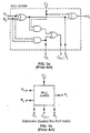
- the delay from the application of the input signals (A's and B's) to the appearance of a valid signal at the generate outputs (G i 's) and propagate outputs (P i 's) of an adder stage is 1 gate (this can be discerned from Fig. 1a).
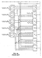
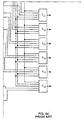
- the delay added in Fig. 3 by the carry restorer portion of the look ahead carry circuitry is 2 gates, which makes a total of a 3-gate delay from the application of the input signals to the adder until the last carry-out bit is available. This relationship is independent of the number of bits being added. For a multibit adder circuit, the delay will be significantly less than the delay of a conventional ripple carry adder circuit.
- a programmable logic device comprising an array of logic blocks, each logic block having:
- the fast carry path receives the above C i function and generates the above C i+1 function.
- the XOR functions of A i and B i in the above equations are generated by look-up table function generators.
- the carry path is implemented in an array, with the carry out of one bit connected to the carry achieved.
- an XOR gate is also provided so that the sum function S i can be completed without requiring more than one function generator for one bit.
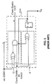
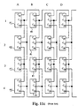
- Fig. 11c is a schematic diagram showing one embodiment of dedicated carry logic interconnect circuitry.
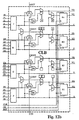
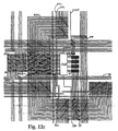
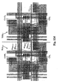
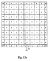
- Fig. 12c shows a tile which combines the CLB of Fig. 12a or 12b with interconnect routing for interconnecting an array of CLBs.
- Figs. 10, 11a, 11b, and 11c show circuit diagrams used in the Xilinx XC4000 family devices for implementing the structure of Fig. 8a.
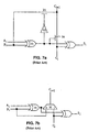
- the signal from F1 is propagated to C 1 if transistor T102 (equivalent to transistor 93 of Fig 7a) turns on in response to A 0 being equal to B 0 .
- Setting memory cell CL5 high prevents the value in cell CL7 from simultaneously being propagated to line 105.
- the carry-in can be preset to zero by applying a logic zero to one of Carry-In T or Carry-In B and setting memory cell MC to propagate the signal. (Generating this logic zero signal is discussed below in conjunction with Fig. 11a.)
- transistor T101 is turned off and transistor T102 is turned on (by setting CL3 low and CL2 low) so that one of the three inputs of multiplexer M101 can be used to preset C 1 to logic one.
- Multiplexer M101 can provide the logic one through the F3 terminal by applying a low signal to F3, and setting CL5 high and CL4 low.
- Multiplexer M101 can provide the logic one as a stored value in memory cell CL7 by setting CL7 high, CL5 low, and CL4 low.
- Multiplexer M101 can provide the logic one through the F1 input terminal by applying a high signal on F1, and setting CL5 and CL4 high.
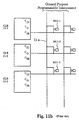
- a multi-bit adder is described with reference to Fig. 11a.
- an ordered array of blocks 1-4 each block comprising a circuit as shown in Fig. 10, is provided such that the carry-out, labeled C i+2 in Fig. 10 and labeled Carry Out on each logic block in Fig. 11a is connected both to the carry-in of the logic block above, labeled Carry In B in both figures and the carry-in of the logic block below, labeled Carry In T in both figures.
- each logic block can selectively receive a carry signal either from the logic block above (on terminal Carry In T ) or the logic block below (on terminal Carry In B ).
- memory cell M11-1 is programmed to turn on its corresponding transistor so that the signal on line 11-a will propagate to terminal C IB of block 11-1. If it is desired to connect output C 0 to logic block. 11-3, memory cell M11-3 is turned on to connect interconnect line 11-a to input C IT of logic block 11-3.
- Other memory cells can likewise be programmed to control the direction of signal propagation from one logic block to the next. It is easy to see that a large number of memory cells is needed in order to provide flexibility in controlling the propagation direction of the carry signal through the stages of a multi-bit adder.
- pins F0 through F3 may have one of two beneficial effects.
- a low number of PIPs can provide sufficient interconnectability. Since each PIP requires about six transistors, reducing the number of PIPs reduces the size of the chip. Alternatively, if more PIPs are provided, a fast route for all function generator inputs is generally available, and therefore the chip operation is faster.
Landscapes
- Physics & Mathematics (AREA)
- Mathematical Physics (AREA)
- Engineering & Computer Science (AREA)
- General Engineering & Computer Science (AREA)
- Computing Systems (AREA)
- Computer Hardware Design (AREA)
- General Physics & Mathematics (AREA)
- Mathematical Analysis (AREA)
- Theoretical Computer Science (AREA)
- Pure & Applied Mathematics (AREA)
- Computational Mathematics (AREA)
- Mathematical Optimization (AREA)
- Logic Circuits (AREA)
Applications Claiming Priority (3)
| Application Number | Priority Date | Filing Date | Title |
|---|---|---|---|
| US08/116,659 US5349250A (en) | 1993-09-02 | 1993-09-02 | Logic structure and circuit for fast carry |
| US116659 | 1993-09-02 | ||
| EP94926045A EP0667059B1 (fr) | 1993-09-02 | 1994-08-31 | Structure et circuit logiques pour report rapide |
Related Parent Applications (1)
| Application Number | Title | Priority Date | Filing Date |
|---|---|---|---|
| EP94926045A Division EP0667059B1 (fr) | 1993-09-02 | 1994-08-31 | Structure et circuit logiques pour report rapide |
Publications (2)
| Publication Number | Publication Date |
|---|---|
| EP1126613A2 true EP1126613A2 (fr) | 2001-08-22 |
| EP1126613A3 EP1126613A3 (fr) | 2006-04-05 |
Family
ID=22368495
Family Applications (2)
| Application Number | Title | Priority Date | Filing Date |
|---|---|---|---|
| EP00115392A Withdrawn EP1126613A3 (fr) | 1993-09-02 | 1994-08-31 | Structure logique et circuit pour report rapide |
| EP94926045A Expired - Lifetime EP0667059B1 (fr) | 1993-09-02 | 1994-08-31 | Structure et circuit logiques pour report rapide |
Family Applications After (1)
| Application Number | Title | Priority Date | Filing Date |
|---|---|---|---|
| EP94926045A Expired - Lifetime EP0667059B1 (fr) | 1993-09-02 | 1994-08-31 | Structure et circuit logiques pour report rapide |
Country Status (5)
| Country | Link |
|---|---|
| US (1) | US5349250A (fr) |
| EP (2) | EP1126613A3 (fr) |
| JP (1) | JP3594601B2 (fr) |
| DE (1) | DE69429073T2 (fr) |
| WO (1) | WO1995006979A1 (fr) |
Cited By (1)
| Publication number | Priority date | Publication date | Assignee | Title |
|---|---|---|---|---|
| RU2445680C1 (ru) * | 2010-11-03 | 2012-03-20 | Лев Петрович Петренко | ФУНКЦИОНАЛЬНАЯ СТРУКТУРА СКВОЗНОГО ПЕРЕНОСА f1(←←)i+1 И f2(←←)i УСЛОВНО "i+1" И УСЛОВНО "i" РАЗРЯДОВ "k" ГРУППЫ АРГУМЕНТОВ МНОЖИМОГО [ni]f(2n) ПРЕДВАРИТЕЛЬНОГО СУММАТОРА fΣ([ni]&[ni,0]) ПАРАЛЛЕЛЬНО-ПОСЛЕДОВАТЕЛЬНОГО УМНОЖИТЕЛЯ fΣ(Σ) (ВАРИАНТЫ) |
Families Citing this family (223)
| Publication number | Priority date | Publication date | Assignee | Title |
|---|---|---|---|---|
| US5122685A (en) * | 1991-03-06 | 1992-06-16 | Quicklogic Corporation | Programmable application specific integrated circuit and logic cell therefor |
| US5416367A (en) * | 1991-03-06 | 1995-05-16 | Quicklogic Corporation | Programmable application specific integrated circuit and logic cell therefor |
| US5550782A (en) * | 1991-09-03 | 1996-08-27 | Altera Corporation | Programmable logic array integrated circuits |
| US5633830A (en) * | 1995-11-08 | 1997-05-27 | Altera Corporation | Random access memory block circuitry for programmable logic array integrated circuit devices |
| USRE35977E (en) * | 1992-05-08 | 1998-12-01 | Altera Corporation | Look up table implementation of fast carry arithmetic and exclusive-or operations |
| US5546018A (en) * | 1993-09-02 | 1996-08-13 | Xilinx, Inc. | Fast carry structure with synchronous input |
| US5629886A (en) * | 1993-09-02 | 1997-05-13 | Xilinx, Inc. | Method and structure for providing fast propagation of a carry signal in a field programmable gate array |
| US6154053A (en) * | 1993-09-02 | 2000-11-28 | Xilinx, Inc. | Look-ahead carry structure with homogeneous CLB structure and pitch larger than CLB pitch |
| US5898319A (en) * | 1993-09-02 | 1999-04-27 | Xilinx, Inc. | Method and structure for providing fast conditional sum in a field programmable gate array |
| US6288570B1 (en) | 1993-09-02 | 2001-09-11 | Xilinx, Inc. | Logic structure and circuit for fast carry |
| US5481206A (en) | 1993-09-02 | 1996-01-02 | Xilinx, Inc. | Circuit for fast carry and logic |
| USRE38451E1 (en) * | 1993-11-12 | 2004-03-02 | Altera Corporation | Universal logic module with arithmetic capabilities |
| US5682107A (en) * | 1994-04-01 | 1997-10-28 | Xilinx, Inc. | FPGA architecture with repeatable tiles including routing matrices and logic matrices |
| US5442306A (en) * | 1994-09-09 | 1995-08-15 | At&T Corp. | Field programmable gate array using look-up tables, multiplexers and decoders |
| US5815003A (en) * | 1994-11-04 | 1998-09-29 | Altera Corporation | Programmable logic integrated circuits with partitioned logic element using shared lab-wide signals |
| US5636368A (en) * | 1994-12-23 | 1997-06-03 | Xilinx, Inc. | Method for programming complex PLD having more than one function block type |
| US5566123A (en) * | 1995-02-10 | 1996-10-15 | Xilinx, Inc. | Synchronous dual port ram |
| US5751162A (en) * | 1995-04-06 | 1998-05-12 | Texas Instruments Incorporated | Field programmable gate array logic module configurable as combinational or sequential circuits |
| US5631576A (en) * | 1995-09-01 | 1997-05-20 | Altera Corporation | Programmable logic array integrated circuit devices with flexible carry chains |
| US5818255A (en) * | 1995-09-29 | 1998-10-06 | Xilinx, Inc. | Method and circuit for using a function generator of a programmable logic device to implement carry logic functions |
| US5672985A (en) * | 1995-12-18 | 1997-09-30 | Altera Corporation | Programmable logic array integrated circuits with carry and/or cascade rings |
| US5898602A (en) * | 1996-01-25 | 1999-04-27 | Xilinx, Inc. | Carry chain circuit with flexible carry function for implementing arithmetic and logical functions |
| US5894565A (en) * | 1996-05-20 | 1999-04-13 | Atmel Corporation | Field programmable gate array with distributed RAM and increased cell utilization |
| US5889413A (en) * | 1996-11-22 | 1999-03-30 | Xilinx, Inc. | Lookup tables which double as shift registers |
| US6297665B1 (en) | 1996-11-22 | 2001-10-02 | Xilinx, Inc. | FPGA architecture with dual-port deep look-up table RAMS |
| US6323682B1 (en) | 1996-11-22 | 2001-11-27 | Xilinx, Inc. | FPGA architecture with wide function multiplexers |
| US6288568B1 (en) | 1996-11-22 | 2001-09-11 | Xilinx, Inc. | FPGA architecture with deep look-up table RAMs |
| US6427156B1 (en) | 1997-01-21 | 2002-07-30 | Xilinx, Inc. | Configurable logic block with AND gate for efficient multiplication in FPGAS |
| US5920202A (en) * | 1997-02-26 | 1999-07-06 | Xilinx, Inc. | Configurable logic element with ability to evaluate five and six input functions |
| US5942913A (en) * | 1997-03-20 | 1999-08-24 | Xilinx, Inc. | FPGA repeatable interconnect structure with bidirectional and unidirectional interconnect lines |
| US6204689B1 (en) | 1997-02-26 | 2001-03-20 | Xilinx, Inc. | Input/output interconnect circuit for FPGAs |
| US5889411A (en) * | 1997-02-26 | 1999-03-30 | Xilinx, Inc. | FPGA having logic element carry chains capable of generating wide XOR functions |
| US5914616A (en) * | 1997-02-26 | 1999-06-22 | Xilinx, Inc. | FPGA repeatable interconnect structure with hierarchical interconnect lines |
| US6201410B1 (en) | 1997-02-26 | 2001-03-13 | Xilinx, Inc. | Wide logic gate implemented in an FPGA configurable logic element |
| US5963050A (en) | 1997-02-26 | 1999-10-05 | Xilinx, Inc. | Configurable logic element with fast feedback paths |
| US6184710B1 (en) | 1997-03-20 | 2001-02-06 | Altera Corporation | Programmable logic array devices with enhanced interconnectivity between adjacent logic regions |
| US6014038A (en) * | 1997-03-21 | 2000-01-11 | Lightspeed Semiconductor Corporation | Function block architecture for gate array |
| US6359466B1 (en) * | 1997-09-16 | 2002-03-19 | Vantis Corporation | Circuitry to provide fast carry |
| US6097212A (en) * | 1997-10-09 | 2000-08-01 | Lattice Semiconductor Corporation | Variable grain architecture for FPGA integrated circuits |
| US6185724B1 (en) | 1997-12-02 | 2001-02-06 | Xilinx, Inc. | Template-based simulated annealing move-set that improves FPGA architectural feature utilization |
| US6069490A (en) * | 1997-12-02 | 2000-05-30 | Xilinx, Inc. | Routing architecture using a direct connect routing mesh |
| US6467017B1 (en) | 1998-06-23 | 2002-10-15 | Altera Corporation | Programmable logic device having embedded dual-port random access memory configurable as single-port memory |
| US6353920B1 (en) * | 1998-11-17 | 2002-03-05 | Xilinx, Inc. | Method for implementing wide gates and tristate buffers using FPGA carry logic |
| US6154052A (en) * | 1999-02-04 | 2000-11-28 | Xilinx, Inc. | Combined tristate/carry logic mechanism |
| US6603332B2 (en) | 1999-02-25 | 2003-08-05 | Xilinx, Inc. | Configurable logic block for PLD with logic gate for combining output with another configurable logic block |
| WO2000052824A1 (fr) | 1999-03-04 | 2000-09-08 | Altera Corporation | Dispositif logique programmable equipe d'un processus d'addition selection-report |
| US6323680B1 (en) | 1999-03-04 | 2001-11-27 | Altera Corporation | Programmable logic device configured to accommodate multiplication |
| US6407576B1 (en) | 1999-03-04 | 2002-06-18 | Altera Corporation | Interconnection and input/output resources for programmable logic integrated circuit devices |
| US6426648B1 (en) | 1999-12-30 | 2002-07-30 | RUPP CHARLé R. | Carry lookahead for programmable logic array |
| US7346644B1 (en) | 2000-09-18 | 2008-03-18 | Altera Corporation | Devices and methods with programmable logic and digital signal processing regions |
| US7119576B1 (en) | 2000-09-18 | 2006-10-10 | Altera Corporation | Devices and methods with programmable logic and digital signal processing regions |
| US6480023B1 (en) | 2000-10-13 | 2002-11-12 | Xilinx, Inc. | Configurable logic block for PLD |
| US6754686B1 (en) | 2000-10-13 | 2004-06-22 | Xilinx, Inc. | Literal sharing method for fast sum-of-products logic |
| US6724810B1 (en) | 2000-11-17 | 2004-04-20 | Xilinx, Inc. | Method and apparatus for de-spreading spread spectrum signals |
| US6369608B1 (en) | 2001-01-18 | 2002-04-09 | Xillinx, Inc. | Conditioning semiconductor-on-insulator transistors for programmable logic devices |
| US6388466B1 (en) | 2001-04-27 | 2002-05-14 | Xilinx, Inc. | FPGA logic element with variable-length shift register capability |
| US6566906B1 (en) * | 2001-09-18 | 2003-05-20 | Altera Corporation | Specialized programmable logic region with low-power mode |
| US6937062B1 (en) | 2001-09-18 | 2005-08-30 | Altera Corporation | Specialized programmable logic region with low-power mode |
| US6857117B2 (en) * | 2002-01-31 | 2005-02-15 | Cadence Design Systems, Inc. | Method and apparatus for producing a circuit description of a design |
| US7028281B1 (en) | 2002-07-12 | 2006-04-11 | Lattice Semiconductor Corporation | FPGA with register-intensive architecture |
| US7111110B1 (en) | 2002-12-10 | 2006-09-19 | Altera Corporation | Versatile RAM for programmable logic device |
| US6798240B1 (en) | 2003-01-24 | 2004-09-28 | Altera Corporation | Logic circuitry with shared lookup table |
| US7800401B1 (en) | 2003-02-10 | 2010-09-21 | Altera Corporation | Fracturable lookup table and logic element |
| US6943580B2 (en) * | 2003-02-10 | 2005-09-13 | Altera Corporation | Fracturable lookup table and logic element |
| US6888373B2 (en) | 2003-02-11 | 2005-05-03 | Altera Corporation | Fracturable incomplete look up table for area efficient logic elements |
| KR101067727B1 (ko) * | 2003-02-19 | 2011-09-28 | 코닌클리즈케 필립스 일렉트로닉스 엔.브이. | 프로그래밍 가능한 논리 셀 어레이를 갖는 전자 회로 |
| US7082592B1 (en) | 2003-06-16 | 2006-07-25 | Altera Corporation | Method for programming programmable logic device having specialized functional blocks |
| US7440964B2 (en) * | 2003-08-29 | 2008-10-21 | Vortaloptics, Inc. | Method, device and software for querying and presenting search results |
| US7185035B1 (en) | 2003-10-23 | 2007-02-27 | Altera Corporation | Arithmetic structures for programmable logic devices |
| US7565388B1 (en) | 2003-11-21 | 2009-07-21 | Altera Corporation | Logic cell supporting addition of three binary words |
| US7167021B1 (en) | 2003-11-24 | 2007-01-23 | Altera Corporation | Logic device logic modules having improved arithmetic circuitry |
| US7071732B1 (en) | 2003-12-09 | 2006-07-04 | Xilinx, Inc. | Scalable complex programmable logic device with segmented interconnect resources |
| US7698358B1 (en) | 2003-12-24 | 2010-04-13 | Altera Corporation | Programmable logic device with specialized functional block |
| US7853632B2 (en) | 2003-12-29 | 2010-12-14 | Xilinx, Inc. | Architectural floorplan for a digital signal processing circuit |
| US7853634B2 (en) | 2003-12-29 | 2010-12-14 | Xilinx, Inc. | Digital signal processing circuit having a SIMD circuit |
| US7467175B2 (en) * | 2003-12-29 | 2008-12-16 | Xilinx, Inc. | Programmable logic device with pipelined DSP slices |
| US7870182B2 (en) | 2003-12-29 | 2011-01-11 | Xilinx Inc. | Digital signal processing circuit having an adder circuit with carry-outs |
| US7567997B2 (en) * | 2003-12-29 | 2009-07-28 | Xilinx, Inc. | Applications of cascading DSP slices |
| US7844653B2 (en) | 2003-12-29 | 2010-11-30 | Xilinx, Inc. | Digital signal processing circuit having a pre-adder circuit |
| US8495122B2 (en) * | 2003-12-29 | 2013-07-23 | Xilinx, Inc. | Programmable device with dynamic DSP architecture |
| US7480690B2 (en) * | 2003-12-29 | 2009-01-20 | Xilinx, Inc. | Arithmetic circuit with multiplexed addend inputs |
| US7472155B2 (en) * | 2003-12-29 | 2008-12-30 | Xilinx, Inc. | Programmable logic device with cascading DSP slices |
| US7860915B2 (en) * | 2003-12-29 | 2010-12-28 | Xilinx, Inc. | Digital signal processing circuit having a pattern circuit for determining termination conditions |
| US7467177B2 (en) * | 2003-12-29 | 2008-12-16 | Xilinx, Inc. | Mathematical circuit with dynamic rounding |
| US7882165B2 (en) * | 2003-12-29 | 2011-02-01 | Xilinx, Inc. | Digital signal processing element having an arithmetic logic unit |
| US7865542B2 (en) * | 2003-12-29 | 2011-01-04 | Xilinx, Inc. | Digital signal processing block having a wide multiplexer |
| US7840630B2 (en) * | 2003-12-29 | 2010-11-23 | Xilinx, Inc. | Arithmetic logic unit circuit |
| US7853636B2 (en) | 2003-12-29 | 2010-12-14 | Xilinx, Inc. | Digital signal processing circuit having a pattern detector circuit for convergent rounding |
| US7840627B2 (en) | 2003-12-29 | 2010-11-23 | Xilinx, Inc. | Digital signal processing circuit having input register blocks |
| US7849119B2 (en) | 2003-12-29 | 2010-12-07 | Xilinx, Inc. | Digital signal processing circuit having a pattern detector circuit |
| US7425841B2 (en) | 2004-02-14 | 2008-09-16 | Tabula Inc. | Configurable circuits, IC's, and systems |
| US7193440B1 (en) | 2004-02-14 | 2007-03-20 | Herman Schmit | Configurable circuits, IC's, and systems |
| US7126373B1 (en) | 2004-02-14 | 2006-10-24 | Herman Schmit | Configurable logic circuits with commutative properties |
| US7284222B1 (en) | 2004-06-30 | 2007-10-16 | Tabula, Inc. | Method and apparatus for identifying connections between configurable nodes in a configurable integrated circuit |
| US7193432B1 (en) | 2004-02-14 | 2007-03-20 | Herman Schmit | VPA logic circuits |
| US7157933B1 (en) | 2004-02-14 | 2007-01-02 | Herman Schmit | Configurable circuits, IC's, and systems |
| US7109752B1 (en) * | 2004-02-14 | 2006-09-19 | Herman Schmit | Configurable circuits, IC's, and systems |
| US7126381B1 (en) | 2004-02-14 | 2006-10-24 | Herman Schmit | VPA interconnect circuit |
| US7167025B1 (en) | 2004-02-14 | 2007-01-23 | Herman Schmit | Non-sequentially configurable IC |
| US7205791B1 (en) | 2004-03-12 | 2007-04-17 | Altera Corporation | Bypass-able carry chain in a programmable logic device |
| US7061268B1 (en) | 2004-03-15 | 2006-06-13 | Altera Corporation | Initializing a carry chain in a programmable logic device |
| US7167022B1 (en) | 2004-03-25 | 2007-01-23 | Altera Corporation | Omnibus logic element including look up table based logic elements |
| US7408382B2 (en) * | 2004-06-30 | 2008-08-05 | Tabula, Inc. | Configurable circuits, IC's, and systems |
| US7439766B2 (en) * | 2004-06-30 | 2008-10-21 | Tabula, Inc. | Configurable logic circuits with commutative properties |
| US7193438B1 (en) | 2004-06-30 | 2007-03-20 | Andre Rohe | Configurable integrated circuit with offset connection |
| US7449915B2 (en) * | 2004-06-30 | 2008-11-11 | Tabula Inc. | VPA logic circuits |
| US7282950B1 (en) | 2004-11-08 | 2007-10-16 | Tabula, Inc. | Configurable IC's with logic resources with offset connections |
| US7312630B2 (en) | 2004-06-30 | 2007-12-25 | Tabula, Inc. | Configurable integrated circuit with built-in turns |
| US7145361B1 (en) | 2004-06-30 | 2006-12-05 | Andre Rohe | Configurable integrated circuit with different connection schemes |
| US7617269B2 (en) * | 2004-08-03 | 2009-11-10 | Stmicroelectronics Pvt. Ltd. | Logic entity with two outputs for efficient adder and other macro implementations |
| US7330050B2 (en) | 2004-11-08 | 2008-02-12 | Tabula, Inc. | Storage elements for a configurable IC and method and apparatus for accessing data stored in the storage elements |
| US7242216B1 (en) | 2004-11-08 | 2007-07-10 | Herman Schmit | Embedding memory between tile arrangement of a configurable IC |
| US7224181B1 (en) * | 2004-11-08 | 2007-05-29 | Herman Schmit | Clock distribution in a configurable IC |
| US7259587B1 (en) * | 2004-11-08 | 2007-08-21 | Tabula, Inc. | Configurable IC's with configurable logic resources that have asymetric inputs and/or outputs |
| US7317331B2 (en) | 2004-11-08 | 2008-01-08 | Tabula, Inc. | Reconfigurable IC that has sections running at different reconfiguration rates |
| US7295037B2 (en) * | 2004-11-08 | 2007-11-13 | Tabula, Inc. | Configurable IC with routing circuits with offset connections |
| US20070244958A1 (en) * | 2004-11-08 | 2007-10-18 | Jason Redgrave | Configurable IC's with carry bypass circuitry |
| US7573296B2 (en) | 2004-11-08 | 2009-08-11 | Tabula Inc. | Configurable IC with configurable routing resources that have asymmetric input and/or outputs |
| US7276933B1 (en) | 2004-11-08 | 2007-10-02 | Tabula, Inc. | Reconfigurable IC that has sections running at different looperness |
| US7917559B2 (en) * | 2004-11-08 | 2011-03-29 | Tabula, Inc. | Configurable IC's with configurable logic circuits that perform adder and/or subtractor operations |
| US7342415B2 (en) | 2004-11-08 | 2008-03-11 | Tabula, Inc. | Configurable IC with interconnect circuits that also perform storage operations |
| US7301368B2 (en) | 2005-03-15 | 2007-11-27 | Tabula, Inc. | Embedding memory within tile arrangement of a configurable IC |
| US7743085B2 (en) | 2004-11-08 | 2010-06-22 | Tabula, Inc. | Configurable IC with large carry chains |
| US7268586B1 (en) | 2004-11-08 | 2007-09-11 | Tabula, Inc. | Method and apparatus for accessing stored data in a reconfigurable IC |
| US7236009B1 (en) | 2004-12-01 | 2007-06-26 | Andre Rohe | Operational time extension |
| US7496879B2 (en) * | 2004-12-01 | 2009-02-24 | Tabula, Inc. | Concurrent optimization of physical design and operational cycle assignment |
| US7428721B2 (en) * | 2004-12-01 | 2008-09-23 | Tabula, Inc. | Operational cycle assignment in a configurable IC |
| US7653677B1 (en) * | 2005-01-26 | 2010-01-26 | Xilinx, Inc. | Digital logic circuit for adding three binary words and method of implementing same |
| US7298169B2 (en) * | 2005-03-15 | 2007-11-20 | Tabula, Inc | Hybrid logic/interconnect circuit in a configurable IC |
| US7825684B2 (en) | 2005-03-15 | 2010-11-02 | Tabula, Inc. | Variable width management for a memory of a configurable IC |
| US7530033B2 (en) * | 2005-03-15 | 2009-05-05 | Tabula, Inc. | Method and apparatus for decomposing functions in a configurable IC |
| US7230869B1 (en) | 2005-03-15 | 2007-06-12 | Jason Redgrave | Method and apparatus for accessing contents of memory cells |
| US7310003B2 (en) * | 2005-03-15 | 2007-12-18 | Tabula, Inc. | Configurable IC with interconnect circuits that have select lines driven by user signals |
| US7224182B1 (en) | 2005-03-15 | 2007-05-29 | Brad Hutchings | Hybrid configurable circuit for a configurable IC |
| US20070244959A1 (en) * | 2005-03-15 | 2007-10-18 | Steven Teig | Configurable IC's with dual carry chains |
| US8620980B1 (en) | 2005-09-27 | 2013-12-31 | Altera Corporation | Programmable device with specialized multiplier blocks |
| US7818361B1 (en) | 2005-11-07 | 2010-10-19 | Tabula, Inc. | Method and apparatus for performing two's complement multiplication |
| US7372297B1 (en) | 2005-11-07 | 2008-05-13 | Tabula Inc. | Hybrid interconnect/logic circuits enabling efficient replication of a function in several sub-cycles to save logic and routing resources |
| US8463836B1 (en) | 2005-11-07 | 2013-06-11 | Tabula, Inc. | Performing mathematical and logical operations in multiple sub-cycles |
| US7765249B1 (en) | 2005-11-07 | 2010-07-27 | Tabula, Inc. | Use of hybrid interconnect/logic circuits for multiplication |
| US7461362B1 (en) | 2005-12-01 | 2008-12-02 | Tabula, Inc. | Replacing circuit design elements with their equivalents |
| US7489162B1 (en) | 2005-12-01 | 2009-02-10 | Tabula, Inc. | Users registers in a reconfigurable IC |
| US7679401B1 (en) | 2005-12-01 | 2010-03-16 | Tabula, Inc. | User registers implemented with routing circuits in a configurable IC |
| US8041759B1 (en) | 2006-02-09 | 2011-10-18 | Altera Corporation | Specialized processing block for programmable logic device |
| US8301681B1 (en) | 2006-02-09 | 2012-10-30 | Altera Corporation | Specialized processing block for programmable logic device |
| US8266198B2 (en) | 2006-02-09 | 2012-09-11 | Altera Corporation | Specialized processing block for programmable logic device |
| US8266199B2 (en) | 2006-02-09 | 2012-09-11 | Altera Corporation | Specialized processing block for programmable logic device |
| US7694083B1 (en) | 2006-03-08 | 2010-04-06 | Tabula, Inc. | System and method for providing a virtual memory architecture narrower and deeper than a physical memory architecture |
| US7797497B1 (en) | 2006-03-08 | 2010-09-14 | Tabula, Inc. | System and method for providing more logical memory ports than physical memory ports |
| US7504858B1 (en) | 2006-03-08 | 2009-03-17 | Tabula, Inc. | Configurable integrated circuit with parallel non-neighboring offset connections |
| US7609085B1 (en) | 2006-03-08 | 2009-10-27 | Tabula, Inc. | Configurable integrated circuit with a 4-to-1 multiplexer |
| US7518400B1 (en) | 2006-03-08 | 2009-04-14 | Tabula, Inc. | Barrel shifter implemented on a configurable integrated circuit |
| US7669097B1 (en) | 2006-03-27 | 2010-02-23 | Tabula, Inc. | Configurable IC with error detection and correction circuitry |
| US7529992B1 (en) | 2006-03-27 | 2009-05-05 | Tabula, Inc. | Configurable integrated circuit with error correcting circuitry |
| US8707225B1 (en) * | 2006-04-07 | 2014-04-22 | Cadence Design Systems, Inc. | Synthesis of area-efficient subtractor and divider functional blocks |
| US7836117B1 (en) | 2006-04-07 | 2010-11-16 | Altera Corporation | Specialized processing block for programmable logic device |
| US7822799B1 (en) | 2006-06-26 | 2010-10-26 | Altera Corporation | Adder-rounder circuitry for specialized processing block in programmable logic device |
| US8386550B1 (en) | 2006-09-20 | 2013-02-26 | Altera Corporation | Method for configuring a finite impulse response filter in a programmable logic device |
| US7930336B2 (en) | 2006-12-05 | 2011-04-19 | Altera Corporation | Large multiplier for programmable logic device |
| US8386553B1 (en) | 2006-12-05 | 2013-02-26 | Altera Corporation | Large multiplier for programmable logic device |
| US7930666B1 (en) | 2006-12-12 | 2011-04-19 | Tabula, Inc. | System and method of providing a memory hierarchy |
| US7587697B1 (en) | 2006-12-12 | 2009-09-08 | Tabula, Inc. | System and method of mapping memory blocks in a configurable integrated circuit |
| US7814137B1 (en) | 2007-01-09 | 2010-10-12 | Altera Corporation | Combined interpolation and decimation filter for programmable logic device |
| US8650231B1 (en) | 2007-01-22 | 2014-02-11 | Altera Corporation | Configuring floating point operations in a programmable device |
| US7865541B1 (en) | 2007-01-22 | 2011-01-04 | Altera Corporation | Configuring floating point operations in a programmable logic device |
| US8645450B1 (en) | 2007-03-02 | 2014-02-04 | Altera Corporation | Multiplier-accumulator circuitry and methods |
| US7525344B2 (en) | 2007-03-20 | 2009-04-28 | Tabula, Inc. | Configurable IC having a routing fabric with storage elements |
| US7535252B1 (en) | 2007-03-22 | 2009-05-19 | Tabula, Inc. | Configurable ICs that conditionally transition through configuration data sets |
| US7772879B1 (en) | 2007-04-11 | 2010-08-10 | Actel Corporation | Logic module including versatile adder for FPGA |
| US7733124B1 (en) * | 2007-06-22 | 2010-06-08 | Altera Corporation | Method and apparatus for PLD having shared storage elements |
| US7949699B1 (en) | 2007-08-30 | 2011-05-24 | Altera Corporation | Implementation of decimation filter in integrated circuit device using ram-based data storage |
| EP2201569A4 (fr) | 2007-09-06 | 2011-07-13 | Tabula Inc | Commutateur de contexte de configuration |
| US7663400B1 (en) * | 2007-12-21 | 2010-02-16 | Actel Corporation | Flexible carry scheme for field programmable gate arrays |
| US8244791B1 (en) | 2008-01-30 | 2012-08-14 | Actel Corporation | Fast carry lookahead circuits |
| US8863067B1 (en) | 2008-02-06 | 2014-10-14 | Tabula, Inc. | Sequential delay analysis by placement engines |
| US8959137B1 (en) | 2008-02-20 | 2015-02-17 | Altera Corporation | Implementing large multipliers in a programmable integrated circuit device |
| US8244789B1 (en) | 2008-03-14 | 2012-08-14 | Altera Corporation | Normalization of floating point operations in a programmable integrated circuit device |
| US7746100B2 (en) * | 2008-04-28 | 2010-06-29 | Altera Corporation | Flexible adder circuits with fast carry chain circuitry |
| US8166435B2 (en) | 2008-06-26 | 2012-04-24 | Tabula, Inc. | Timing operations in an IC with configurable circuits |
| US8626815B1 (en) | 2008-07-14 | 2014-01-07 | Altera Corporation | Configuring a programmable integrated circuit device to perform matrix multiplication |
| US8255448B1 (en) | 2008-10-02 | 2012-08-28 | Altera Corporation | Implementing division in a programmable integrated circuit device |
| US8307023B1 (en) | 2008-10-10 | 2012-11-06 | Altera Corporation | DSP block for implementing large multiplier on a programmable integrated circuit device |
| US8479133B2 (en) | 2009-01-27 | 2013-07-02 | Xilinx, Inc. | Method of and circuit for implementing a filter in an integrated circuit |
| US8543635B2 (en) | 2009-01-27 | 2013-09-24 | Xilinx, Inc. | Digital signal processing block with preadder stage |
| US8468192B1 (en) | 2009-03-03 | 2013-06-18 | Altera Corporation | Implementing multipliers in a programmable integrated circuit device |
| US8805916B2 (en) | 2009-03-03 | 2014-08-12 | Altera Corporation | Digital signal processing circuitry with redundancy and bidirectional data paths |
| US8645449B1 (en) | 2009-03-03 | 2014-02-04 | Altera Corporation | Combined floating point adder and subtractor |
| US8886696B1 (en) | 2009-03-03 | 2014-11-11 | Altera Corporation | Digital signal processing circuitry with redundancy and ability to support larger multipliers |
| US8549055B2 (en) | 2009-03-03 | 2013-10-01 | Altera Corporation | Modular digital signal processing circuitry with optionally usable, dedicated connections between modules of the circuitry |
| US8706790B1 (en) | 2009-03-03 | 2014-04-22 | Altera Corporation | Implementing mixed-precision floating-point operations in a programmable integrated circuit device |
| US8650236B1 (en) | 2009-08-04 | 2014-02-11 | Altera Corporation | High-rate interpolation or decimation filter in integrated circuit device |
| US8396914B1 (en) | 2009-09-11 | 2013-03-12 | Altera Corporation | Matrix decomposition in an integrated circuit device |
| US8412756B1 (en) | 2009-09-11 | 2013-04-02 | Altera Corporation | Multi-operand floating point operations in a programmable integrated circuit device |
| US8539016B1 (en) | 2010-02-09 | 2013-09-17 | Altera Corporation | QR decomposition in an integrated circuit device |
| US7948267B1 (en) | 2010-02-09 | 2011-05-24 | Altera Corporation | Efficient rounding circuits and methods in configurable integrated circuit devices |
| US8601044B2 (en) | 2010-03-02 | 2013-12-03 | Altera Corporation | Discrete Fourier Transform in an integrated circuit device |
| US8458243B1 (en) | 2010-03-03 | 2013-06-04 | Altera Corporation | Digital signal processing circuit blocks with support for systolic finite-impulse-response digital filtering |
| US8484265B1 (en) | 2010-03-04 | 2013-07-09 | Altera Corporation | Angular range reduction in an integrated circuit device |
| US8510354B1 (en) | 2010-03-12 | 2013-08-13 | Altera Corporation | Calculation of trigonometric functions in an integrated circuit device |
| US8539014B2 (en) | 2010-03-25 | 2013-09-17 | Altera Corporation | Solving linear matrices in an integrated circuit device |
| US8589463B2 (en) | 2010-06-25 | 2013-11-19 | Altera Corporation | Calculation of trigonometric functions in an integrated circuit device |
| US8862650B2 (en) | 2010-06-25 | 2014-10-14 | Altera Corporation | Calculation of trigonometric functions in an integrated circuit device |
| US8577951B1 (en) | 2010-08-19 | 2013-11-05 | Altera Corporation | Matrix operations in an integrated circuit device |
| US8645451B2 (en) | 2011-03-10 | 2014-02-04 | Altera Corporation | Double-clocked specialized processing block in an integrated circuit device |
| US9600278B1 (en) | 2011-05-09 | 2017-03-21 | Altera Corporation | Programmable device using fixed and configurable logic to implement recursive trees |
| US8812576B1 (en) | 2011-09-12 | 2014-08-19 | Altera Corporation | QR decomposition in an integrated circuit device |
| US9053045B1 (en) | 2011-09-16 | 2015-06-09 | Altera Corporation | Computing floating-point polynomials in an integrated circuit device |
| US8949298B1 (en) | 2011-09-16 | 2015-02-03 | Altera Corporation | Computing floating-point polynomials in an integrated circuit device |
| US8762443B1 (en) | 2011-11-15 | 2014-06-24 | Altera Corporation | Matrix operations in an integrated circuit device |
| US8543634B1 (en) | 2012-03-30 | 2013-09-24 | Altera Corporation | Specialized processing block for programmable integrated circuit device |
| US9098332B1 (en) | 2012-06-01 | 2015-08-04 | Altera Corporation | Specialized processing block with fixed- and floating-point structures |
| US8996600B1 (en) | 2012-08-03 | 2015-03-31 | Altera Corporation | Specialized processing block for implementing floating-point multiplier with subnormal operation support |
| US9207909B1 (en) | 2012-11-26 | 2015-12-08 | Altera Corporation | Polynomial calculations optimized for programmable integrated circuit device structures |
| US9189200B1 (en) | 2013-03-14 | 2015-11-17 | Altera Corporation | Multiple-precision processing block in a programmable integrated circuit device |
| US9348795B1 (en) | 2013-07-03 | 2016-05-24 | Altera Corporation | Programmable device using fixed and configurable logic to implement floating-point rounding |
| US9379687B1 (en) | 2014-01-14 | 2016-06-28 | Altera Corporation | Pipelined systolic finite impulse response filter |
| US9684488B2 (en) | 2015-03-26 | 2017-06-20 | Altera Corporation | Combined adder and pre-adder for high-radix multiplier circuit |
| US9785405B2 (en) * | 2015-05-29 | 2017-10-10 | Huawei Technologies Co., Ltd. | Increment/decrement apparatus and method |
| EP3347990B1 (fr) * | 2015-09-11 | 2019-07-10 | Xilinx, Inc. | Circuit avec lookup-table (lut) et carry logic cascadés |
| US10942706B2 (en) | 2017-05-05 | 2021-03-09 | Intel Corporation | Implementation of floating-point trigonometric functions in an integrated circuit device |
| CN111104101A (zh) * | 2019-11-07 | 2020-05-05 | 上海精密计量测试研究所 | 一种带有slice空洞的进位链构造及测试方法 |
| US11714607B2 (en) | 2020-12-28 | 2023-08-01 | Achronix Semiconductor Corporation | Adder circuit using lookup tables |
| CN116719772B (zh) * | 2023-05-06 | 2024-10-01 | 深圳市紫光同创电子有限公司 | 可编程逻辑电路 |
Family Cites Families (12)
| Publication number | Priority date | Publication date | Assignee | Title |
|---|---|---|---|---|
| US4124899A (en) * | 1977-05-23 | 1978-11-07 | Monolithic Memories, Inc. | Programmable array logic circuit |
| US4870302A (en) * | 1984-03-12 | 1989-09-26 | Xilinx, Inc. | Configurable electrical circuit having configurable logic elements and configurable interconnects |
| US4706216A (en) * | 1985-02-27 | 1987-11-10 | Xilinx, Inc. | Configurable logic element |
| US4758745B1 (en) * | 1986-09-19 | 1994-11-15 | Actel Corp | User programmable integrated circuit interconnect architecture and test method |
| CA2037142C (fr) * | 1990-05-10 | 1996-05-07 | Hung-Cheng Hsieh | Structure et circuits logiques de report rapide |
| US5267187A (en) * | 1990-05-10 | 1993-11-30 | Xilinx Inc | Logic structure and circuit for fast carry |
| US5198705A (en) * | 1990-05-11 | 1993-03-30 | Actel Corporation | Logic module with configurable combinational and sequential blocks |
| US5055718A (en) * | 1990-05-11 | 1991-10-08 | Actel Corporation | Logic module with configurable combinational and sequential blocks |
| US5220213A (en) * | 1991-03-06 | 1993-06-15 | Quicklogic Corporation | Programmable application specific integrated circuit and logic cell therefor |
| US5260611A (en) * | 1991-09-03 | 1993-11-09 | Altera Corporation | Programmable logic array having local and long distance conductors |
| US5359242A (en) * | 1993-01-21 | 1994-10-25 | Altera Corporation | Programmable logic with carry-in/carry-out between logic blocks |
| US5258668A (en) * | 1992-05-08 | 1993-11-02 | Altera Corporation | Programmable logic array integrated circuits with cascade connections between logic modules |
-
1993
- 1993-09-02 US US08/116,659 patent/US5349250A/en not_active Expired - Lifetime
-
1994
- 1994-08-31 DE DE69429073T patent/DE69429073T2/de not_active Expired - Lifetime
- 1994-08-31 EP EP00115392A patent/EP1126613A3/fr not_active Withdrawn
- 1994-08-31 EP EP94926045A patent/EP0667059B1/fr not_active Expired - Lifetime
- 1994-08-31 WO PCT/US1994/009864 patent/WO1995006979A1/fr not_active Ceased
- 1994-08-31 JP JP50826095A patent/JP3594601B2/ja not_active Expired - Lifetime
Cited By (1)
| Publication number | Priority date | Publication date | Assignee | Title |
|---|---|---|---|---|
| RU2445680C1 (ru) * | 2010-11-03 | 2012-03-20 | Лев Петрович Петренко | ФУНКЦИОНАЛЬНАЯ СТРУКТУРА СКВОЗНОГО ПЕРЕНОСА f1(←←)i+1 И f2(←←)i УСЛОВНО "i+1" И УСЛОВНО "i" РАЗРЯДОВ "k" ГРУППЫ АРГУМЕНТОВ МНОЖИМОГО [ni]f(2n) ПРЕДВАРИТЕЛЬНОГО СУММАТОРА fΣ([ni]&[ni,0]) ПАРАЛЛЕЛЬНО-ПОСЛЕДОВАТЕЛЬНОГО УМНОЖИТЕЛЯ fΣ(Σ) (ВАРИАНТЫ) |
Also Published As
| Publication number | Publication date |
|---|---|
| EP0667059B1 (fr) | 2001-11-14 |
| DE69429073T2 (de) | 2002-03-21 |
| JPH08503570A (ja) | 1996-04-16 |
| EP0667059A1 (fr) | 1995-08-16 |
| EP1126613A3 (fr) | 2006-04-05 |
| DE69429073D1 (de) | 2001-12-20 |
| US5349250A (en) | 1994-09-20 |
| WO1995006979A1 (fr) | 1995-03-09 |
| JP3594601B2 (ja) | 2004-12-02 |
Similar Documents
| Publication | Publication Date | Title |
|---|---|---|
| EP0667059B1 (fr) | Structure et circuit logiques pour report rapide | |
| US5481206A (en) | Circuit for fast carry and logic | |
| US6288570B1 (en) | Logic structure and circuit for fast carry | |
| US5523963A (en) | Logic structure and circuit for fast carry | |
| US5546018A (en) | Fast carry structure with synchronous input | |
| CA2037142C (fr) | Structure et circuits logiques de report rapide | |
| US5724276A (en) | Logic block structure optimized for sum generation | |
| US6188240B1 (en) | Programmable function block | |
| US7663400B1 (en) | Flexible carry scheme for field programmable gate arrays | |
| US6369610B1 (en) | Reconfigurable multiplier array | |
| EP0607657B1 (fr) | Dispositif logique programmable et méthode d'utilisation | |
| US6553395B2 (en) | Reconfigurable processor devices | |
| EP1271474B1 (fr) | Bloc fonctionnel | |
| US9292474B1 (en) | Configurable hybrid adder circuitry | |
| US6411980B2 (en) | Data split parallel shifter and parallel adder/subtractor | |
| EP1076931A1 (fr) | Dispositif logique programmable equipe d'un processus d'addition selection-report | |
| US5295090A (en) | Logic structure and circuit for fast carry | |
| US4441158A (en) | Arithmetic operation circuit | |
| US7617269B2 (en) | Logic entity with two outputs for efficient adder and other macro implementations | |
| US6353920B1 (en) | Method for implementing wide gates and tristate buffers using FPGA carry logic | |
| US5661660A (en) | Method for providing multiple function symbols | |
| US6263482B1 (en) | Programmable logic device having macrocells with selectable product-term inversion | |
| JP2000089937A (ja) | ファンアウトの減少したア―キテクチャを備える桁上げ先見加算器 | |
| JP2553162B2 (ja) | 加算回路 | |
| CN114840169A (zh) | 结合行波进位加法器与可路由传播/生成信号在fpga上构建动态块大小进位跳跃加法器 |
Legal Events
| Date | Code | Title | Description |
|---|---|---|---|
| PUAI | Public reference made under article 153(3) epc to a published international application that has entered the european phase |
Free format text: ORIGINAL CODE: 0009012 |
|
| 17P | Request for examination filed |
Effective date: 20000717 |
|
| AC | Divisional application: reference to earlier application |
Ref document number: 667059 Country of ref document: EP |
|
| AK | Designated contracting states |
Kind code of ref document: A2 Designated state(s): DE FR GB |
|
| PUAL | Search report despatched |
Free format text: ORIGINAL CODE: 0009013 |
|
| AK | Designated contracting states |
Kind code of ref document: A3 Designated state(s): DE FR GB |
|
| RIC1 | Information provided on ipc code assigned before grant |
Ipc: G06F 7/50 20060101ALI20060214BHEP Ipc: H03K 19/177 20060101AFI20010628BHEP |
|
| STAA | Information on the status of an ep patent application or granted ep patent |
Free format text: STATUS: THE APPLICATION HAS BEEN WITHDRAWN |
|
| 18W | Application withdrawn |
Effective date: 20060608 |