EP1127962B1 - Verfahren zur herstellung eines siliziumeinkristalls damit hergestellter siliziumeinkristall und siliziumwafer - Google Patents
Verfahren zur herstellung eines siliziumeinkristalls damit hergestellter siliziumeinkristall und siliziumwafer Download PDFInfo
- Publication number
- EP1127962B1 EP1127962B1 EP00956805A EP00956805A EP1127962B1 EP 1127962 B1 EP1127962 B1 EP 1127962B1 EP 00956805 A EP00956805 A EP 00956805A EP 00956805 A EP00956805 A EP 00956805A EP 1127962 B1 EP1127962 B1 EP 1127962B1
- Authority
- EP
- European Patent Office
- Prior art keywords
- crystal
- single crystal
- silicon single
- defects
- temperature zone
- Prior art date
- Legal status (The legal status is an assumption and is not a legal conclusion. Google has not performed a legal analysis and makes no representation as to the accuracy of the status listed.)
- Expired - Lifetime
Links
- 239000013078 crystal Substances 0.000 title claims description 227
- XUIMIQQOPSSXEZ-UHFFFAOYSA-N Silicon Chemical compound [Si] XUIMIQQOPSSXEZ-UHFFFAOYSA-N 0.000 title claims description 106
- 229910052710 silicon Inorganic materials 0.000 title claims description 106
- 239000010703 silicon Substances 0.000 title claims description 106
- 238000000034 method Methods 0.000 title claims description 48
- 238000004519 manufacturing process Methods 0.000 title claims description 17
- 230000007547 defect Effects 0.000 claims description 162
- IJGRMHOSHXDMSA-UHFFFAOYSA-N Atomic nitrogen Chemical compound N#N IJGRMHOSHXDMSA-UHFFFAOYSA-N 0.000 claims description 125
- 238000005054 agglomeration Methods 0.000 claims description 95
- 230000002776 aggregation Effects 0.000 claims description 95
- 229910052757 nitrogen Inorganic materials 0.000 claims description 62
- 239000012535 impurity Substances 0.000 claims description 53
- 238000001816 cooling Methods 0.000 claims description 43
- 238000010438 heat treatment Methods 0.000 claims description 33
- 238000009826 distribution Methods 0.000 claims description 28
- 239000007789 gas Substances 0.000 claims description 8
- 230000001590 oxidative effect Effects 0.000 claims description 5
- 235000012431 wafers Nutrition 0.000 description 76
- 238000012360 testing method Methods 0.000 description 20
- XKRFYHLGVUSROY-UHFFFAOYSA-N Argon Chemical compound [Ar] XKRFYHLGVUSROY-UHFFFAOYSA-N 0.000 description 8
- 230000015556 catabolic process Effects 0.000 description 8
- 238000005530 etching Methods 0.000 description 8
- 239000006185 dispersion Substances 0.000 description 7
- 230000000694 effects Effects 0.000 description 7
- KRHYYFGTRYWZRS-UHFFFAOYSA-N Fluorane Chemical compound F KRHYYFGTRYWZRS-UHFFFAOYSA-N 0.000 description 6
- 238000012545 processing Methods 0.000 description 6
- 239000000047 product Substances 0.000 description 6
- 239000010453 quartz Substances 0.000 description 5
- VYPSYNLAJGMNEJ-UHFFFAOYSA-N silicon dioxide Inorganic materials O=[Si]=O VYPSYNLAJGMNEJ-UHFFFAOYSA-N 0.000 description 5
- 239000002344 surface layer Substances 0.000 description 5
- 229910052786 argon Inorganic materials 0.000 description 4
- QVGXLLKOCUKJST-UHFFFAOYSA-N atomic oxygen Chemical compound [O] QVGXLLKOCUKJST-UHFFFAOYSA-N 0.000 description 4
- 230000001276 controlling effect Effects 0.000 description 4
- 239000000463 material Substances 0.000 description 4
- 239000001301 oxygen Substances 0.000 description 4
- 229910052760 oxygen Inorganic materials 0.000 description 4
- 239000000758 substrate Substances 0.000 description 4
- MHAJPDPJQMAIIY-UHFFFAOYSA-N Hydrogen peroxide Chemical compound OO MHAJPDPJQMAIIY-UHFFFAOYSA-N 0.000 description 3
- 230000003247 decreasing effect Effects 0.000 description 3
- -1 i.e. Substances 0.000 description 3
- 238000011835 investigation Methods 0.000 description 3
- 239000011259 mixed solution Substances 0.000 description 3
- 150000004767 nitrides Chemical class 0.000 description 3
- 238000005498 polishing Methods 0.000 description 3
- 230000008569 process Effects 0.000 description 3
- QGZKDVFQNNGYKY-UHFFFAOYSA-N Ammonia Chemical compound N QGZKDVFQNNGYKY-UHFFFAOYSA-N 0.000 description 2
- ZOXJGFHDIHLPTG-UHFFFAOYSA-N Boron Chemical compound [B] ZOXJGFHDIHLPTG-UHFFFAOYSA-N 0.000 description 2
- GRYLNZFGIOXLOG-UHFFFAOYSA-N Nitric acid Chemical compound O[N+]([O-])=O GRYLNZFGIOXLOG-UHFFFAOYSA-N 0.000 description 2
- 229910052796 boron Inorganic materials 0.000 description 2
- 229910052799 carbon Inorganic materials 0.000 description 2
- 238000004140 cleaning Methods 0.000 description 2
- 230000000052 comparative effect Effects 0.000 description 2
- 238000011161 development Methods 0.000 description 2
- 239000001257 hydrogen Substances 0.000 description 2
- 229910052739 hydrogen Inorganic materials 0.000 description 2
- 125000004435 hydrogen atom Chemical class [H]* 0.000 description 2
- 230000006872 improvement Effects 0.000 description 2
- 230000010354 integration Effects 0.000 description 2
- 239000010410 layer Substances 0.000 description 2
- 238000005259 measurement Methods 0.000 description 2
- 239000000155 melt Substances 0.000 description 2
- 229910017604 nitric acid Inorganic materials 0.000 description 2
- 239000002245 particle Substances 0.000 description 2
- 239000004065 semiconductor Substances 0.000 description 2
- 230000001629 suppression Effects 0.000 description 2
- 238000003325 tomography Methods 0.000 description 2
- 238000012546 transfer Methods 0.000 description 2
- XLYOFNOQVPJJNP-UHFFFAOYSA-N water Substances O XLYOFNOQVPJJNP-UHFFFAOYSA-N 0.000 description 2
- VHUUQVKOLVNVRT-UHFFFAOYSA-N Ammonium hydroxide Chemical compound [NH4+].[OH-] VHUUQVKOLVNVRT-UHFFFAOYSA-N 0.000 description 1
- OAICVXFJPJFONN-UHFFFAOYSA-N Phosphorus Chemical compound [P] OAICVXFJPJFONN-UHFFFAOYSA-N 0.000 description 1
- 238000003723 Smelting Methods 0.000 description 1
- 229910021529 ammonia Inorganic materials 0.000 description 1
- 238000004458 analytical method Methods 0.000 description 1
- 239000007864 aqueous solution Substances 0.000 description 1
- 238000000149 argon plasma sintering Methods 0.000 description 1
- 230000005540 biological transmission Effects 0.000 description 1
- 230000008859 change Effects 0.000 description 1
- 238000003776 cleavage reaction Methods 0.000 description 1
- 239000000112 cooling gas Substances 0.000 description 1
- 238000006731 degradation reaction Methods 0.000 description 1
- 230000001066 destructive effect Effects 0.000 description 1
- 229910001873 dinitrogen Inorganic materials 0.000 description 1
- 238000002474 experimental method Methods 0.000 description 1
- 238000007689 inspection Methods 0.000 description 1
- 239000011810 insulating material Substances 0.000 description 1
- 238000005065 mining Methods 0.000 description 1
- 230000002093 peripheral effect Effects 0.000 description 1
- 229910052698 phosphorus Inorganic materials 0.000 description 1
- 239000011574 phosphorus Substances 0.000 description 1
- 229910021420 polycrystalline silicon Inorganic materials 0.000 description 1
- KMUONIBRACKNSN-UHFFFAOYSA-N potassium dichromate Chemical compound [K+].[K+].[O-][Cr](=O)(=O)O[Cr]([O-])(=O)=O KMUONIBRACKNSN-UHFFFAOYSA-N 0.000 description 1
- 239000002244 precipitate Substances 0.000 description 1
- 239000002994 raw material Substances 0.000 description 1
- 230000009467 reduction Effects 0.000 description 1
- 230000001105 regulatory effect Effects 0.000 description 1
- 238000011160 research Methods 0.000 description 1
- 230000007017 scission Effects 0.000 description 1
- 238000004088 simulation Methods 0.000 description 1
- 238000005507 spraying Methods 0.000 description 1
- 239000011800 void material Substances 0.000 description 1
Images
Classifications
-
- C—CHEMISTRY; METALLURGY
- C30—CRYSTAL GROWTH
- C30B—SINGLE-CRYSTAL GROWTH; UNIDIRECTIONAL SOLIDIFICATION OF EUTECTIC MATERIAL OR UNIDIRECTIONAL DEMIXING OF EUTECTOID MATERIAL; REFINING BY ZONE-MELTING OF MATERIAL; PRODUCTION OF A HOMOGENEOUS POLYCRYSTALLINE MATERIAL WITH DEFINED STRUCTURE; SINGLE CRYSTALS OR HOMOGENEOUS POLYCRYSTALLINE MATERIAL WITH DEFINED STRUCTURE; AFTER-TREATMENT OF SINGLE CRYSTALS OR A HOMOGENEOUS POLYCRYSTALLINE MATERIAL WITH DEFINED STRUCTURE; APPARATUS THEREFOR
- C30B15/00—Single-crystal growth by pulling from a melt, e.g. Czochralski method
- C30B15/20—Controlling or regulating
-
- C—CHEMISTRY; METALLURGY
- C30—CRYSTAL GROWTH
- C30B—SINGLE-CRYSTAL GROWTH; UNIDIRECTIONAL SOLIDIFICATION OF EUTECTIC MATERIAL OR UNIDIRECTIONAL DEMIXING OF EUTECTOID MATERIAL; REFINING BY ZONE-MELTING OF MATERIAL; PRODUCTION OF A HOMOGENEOUS POLYCRYSTALLINE MATERIAL WITH DEFINED STRUCTURE; SINGLE CRYSTALS OR HOMOGENEOUS POLYCRYSTALLINE MATERIAL WITH DEFINED STRUCTURE; AFTER-TREATMENT OF SINGLE CRYSTALS OR A HOMOGENEOUS POLYCRYSTALLINE MATERIAL WITH DEFINED STRUCTURE; APPARATUS THEREFOR
- C30B15/00—Single-crystal growth by pulling from a melt, e.g. Czochralski method
- C30B15/20—Controlling or regulating
- C30B15/206—Controlling or regulating the thermal history of growing the ingot
-
- C—CHEMISTRY; METALLURGY
- C30—CRYSTAL GROWTH
- C30B—SINGLE-CRYSTAL GROWTH; UNIDIRECTIONAL SOLIDIFICATION OF EUTECTIC MATERIAL OR UNIDIRECTIONAL DEMIXING OF EUTECTOID MATERIAL; REFINING BY ZONE-MELTING OF MATERIAL; PRODUCTION OF A HOMOGENEOUS POLYCRYSTALLINE MATERIAL WITH DEFINED STRUCTURE; SINGLE CRYSTALS OR HOMOGENEOUS POLYCRYSTALLINE MATERIAL WITH DEFINED STRUCTURE; AFTER-TREATMENT OF SINGLE CRYSTALS OR A HOMOGENEOUS POLYCRYSTALLINE MATERIAL WITH DEFINED STRUCTURE; APPARATUS THEREFOR
- C30B29/00—Single crystals or homogeneous polycrystalline material with defined structure characterised by the material or by their shape
- C30B29/02—Elements
- C30B29/06—Silicon
Definitions
- JP-10330189 discloses a method for detecting temperature distributions in single crystals by finding the location of grown-in defects and assuming that this location was at a temperature of 1100°C.
- the defect size of the wafer obtained by processing is high, the defects can be eliminated by subjecting the wafer to heat treatment, so that wafers having high quality can be produced. Besides, even though the defects are not eliminated and still remain in the surface layer of the wafer, the defect size is extremely small, and therefore the defects hardly give a harmful influence on characteristics of integrated circuit fabricated on the wafer.
- nitrogen can be doped in a silicon single crystal by placing nitride previously in the quartz crucible, feeding nitride into the silicon melt, or using an atmosphere gas containing nitrogen.
- a doping amount in the crystal can be controlled by controlling an amount of nitride, or concentration or time of introduction of nitrogen gas.
- nitrogen concentration can be easily controlled in the above-mentioned range of 0.1 x 10 13 to 8.0 x 10 13 /cm 3 .
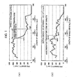
- a single crystal ingot was grown under the same conditions as Example 1, except that a pretest for determining the agglomeration temperature zone with adding nitrogen was not performed and a general hot zone (C type) was used. At this time, a cooling rate of the crystal in the conventional agglomeration temperature zone, i.e., 1100-1010 °C was kept to be 1.9 °C/min, which satisfies a condition for an intended defect size.
Landscapes
- Chemical & Material Sciences (AREA)
- Engineering & Computer Science (AREA)
- Crystallography & Structural Chemistry (AREA)
- Materials Engineering (AREA)
- Metallurgy (AREA)
- Organic Chemistry (AREA)
- Crystals, And After-Treatments Of Crystals (AREA)
- Liquid Deposition Of Substances Of Which Semiconductor Devices Are Composed (AREA)
Claims (8)
- Ein Verfahren zum Herstellen eines Siliziumeinkristalls gemäß einem Czochralski-Verfahren, dadurch gekennzeichnet, dass vor dem Herstellen des Kristalls mit einer vorgegebenen Art und Konzentration von Fremdstoffen ein anderer Siliziumeinkristall mit derselben Art und Konzentration von Fremdstoffen wie der herzustellende Kristall gezüchtet wird, um dadurch eine Agglomerationstemperaturzone seiner eingewachsenen Defekte zu bestimmen, und dann auf der Basis der Temperatur eine Wachstumsbedingung des herzustellenden Kristalls oder eine Temperaturverteilung innerhalb eines Ofens einer Ziehvorrichtung so gesetzt werden, dass eine Abkühlungsgeschwindigkeit des Kristalls zum Durchlaufen der Agglomerationstemperaturzone eine gewünschte Geschwindigkeit zum Herstellen des Siliziumeinkristalls dadurch ist.
- Verfahren zum Herstellen eines Siliziumeinkristalls gemäß Anspruch 1, dadurch gekennzeichnet, dass die Art und Konzentration der Fremdstoffe zumindest Stickstoff und eine Konzentration davon ist.
- Verfahren zum Herstellen eines Siliziumeinkristalls, in dem Stickstoff als Fremdstoff hinzugefügt wird, dadurch gekennzeichnet, dass eine Agglomerationstemperaturzone eingewachsener Defekte des Kristalls, in dem die Stickstoffkonzentration im Bereich von 0,1 x 10¹³ bis 8,0 x 10¹³/cm3 liegt, um -50 °C an der Temperaturobergrenze bzw. um -20 °C an der Temperaturuntergrenze von einer Agglomerationstemperaturzone in einem Fall, in dem kein Stickstoff hinzugefügt ist, verschoben ist, und dann eine Wachstumsbedingung des herzustellenden Kristalls oder eine Temperaturverteilung innerhalb eines Ofens einer Ziehvorrichtung so gesetzt wird, dass eine Abkühlungsgeschwindigkeit des Kristalls zum Durchlaufen der verschobenen Agglomerationstemperaturzone eine gewünschte Geschwindigkeit zum Herstellen des Siliziumeinkristall dadurch ist.
- Verfahren zum Herstellen eines Siliziumeinkristalls gemäß einem der Ansprüche 1 - 3, dadurch gekennzeichnet, dass die durchschnittliche Abkühlungsgeschwindigkeit des Kristalls zum Durchlaufen der Agglomerationstemperaturzone eingewachsener Defekte 1,6 °C/min oder mehr beträgt.
- Verfahren zum Herstellen eines Siliziumeinkristalls gemäß einem der Ansprüche 1 - 3, dadurch gekennzeichnet, dass die durchschnittliche Abkühlungsgeschwindigkeit des Kristalls zum Durchlaufen der Agglomerationstemperaturzone eingewachsener Defekte 1,0 °C/min oder weniger beträgt.
- Verfahren zum Herstellen eines Siliziumeinkristalls gemäß einem der Ansprüche 1 - 4, dadurch gekennzeichnet, dass eine LSTD-Dichte 500 Anzahl/cm2 oder mehr beträgt, bevor er einer Wärmebehandlung ausgesetzt wird.
- Verfahren zum Herstellen eines Siliziumeinkristalls gemäß einem der Ansprüche 1 - 4, dadurch gekennzeichnet, dass die durchschnittliche Größe des eingewachsenen Defekts 70 nm oder weniger beträgt.
- Verfahren zum Herstellen eines Siliziumwafers, der aus einem gemäß dem Verfahren in Anspruch 6 oder Anspruch 7 hergestellten Siliziumeinkristall hergestellt wurde, dadurch gekennzeichnet, dass der Wafer einer Wärmebehandlung in einer Atmosphäre nichtoxidierenden Gases ausgesetzt war.
Applications Claiming Priority (3)
| Application Number | Priority Date | Filing Date | Title |
|---|---|---|---|
| JP24396199 | 1999-08-30 | ||
| JP24396199 | 1999-08-30 | ||
| PCT/JP2000/005873 WO2001016410A1 (fr) | 1999-08-30 | 2000-08-30 | Procede de fabrication de silicium monocristallin, silicium monocristallin fabrique par ce procede et plaquette de silicium |
Publications (3)
| Publication Number | Publication Date |
|---|---|
| EP1127962A1 EP1127962A1 (de) | 2001-08-29 |
| EP1127962A4 EP1127962A4 (de) | 2002-03-20 |
| EP1127962B1 true EP1127962B1 (de) | 2003-12-10 |
Family
ID=17111626
Family Applications (1)
| Application Number | Title | Priority Date | Filing Date |
|---|---|---|---|
| EP00956805A Expired - Lifetime EP1127962B1 (de) | 1999-08-30 | 2000-08-30 | Verfahren zur herstellung eines siliziumeinkristalls damit hergestellter siliziumeinkristall und siliziumwafer |
Country Status (6)
| Country | Link |
|---|---|
| US (1) | US6544332B1 (de) |
| EP (1) | EP1127962B1 (de) |
| JP (1) | JP4154891B2 (de) |
| KR (1) | KR100780097B1 (de) |
| DE (1) | DE60007066T2 (de) |
| WO (1) | WO2001016410A1 (de) |
Families Citing this family (5)
| Publication number | Priority date | Publication date | Assignee | Title |
|---|---|---|---|---|
| US6599360B2 (en) | 2000-01-25 | 2003-07-29 | Shin-Etsu Handotai Co., Ltd. | Silicon wafer, method for determining production conditions of silicon single crystal and method for producing silicon wafer |
| KR101129907B1 (ko) * | 2010-01-25 | 2012-03-23 | 주식회사 엘지실트론 | 단결정 성장방법 |
| CN101792933B (zh) * | 2010-03-10 | 2012-06-06 | 嘉兴明通光能科技有限公司 | 太阳能级硅单晶混合掺杂配料方法 |
| US9212900B2 (en) * | 2012-08-11 | 2015-12-15 | Seagate Technology Llc | Surface features characterization |
| US9377394B2 (en) * | 2012-10-16 | 2016-06-28 | Seagate Technology Llc | Distinguishing foreign surface features from native surface features |
Family Cites Families (13)
| Publication number | Priority date | Publication date | Assignee | Title |
|---|---|---|---|---|
| JPS60251190A (ja) | 1984-05-25 | 1985-12-11 | Shin Etsu Handotai Co Ltd | シリコン単結晶の製造方法 |
| US4981549A (en) * | 1988-02-23 | 1991-01-01 | Mitsubishi Kinzoku Kabushiki Kaisha | Method and apparatus for growing silicon crystals |
| JPH06103714B2 (ja) | 1990-11-22 | 1994-12-14 | 信越半導体株式会社 | シリコン単結晶の電気特性検査方法 |
| JP4097729B2 (ja) | 1996-05-22 | 2008-06-11 | Sumco Techxiv株式会社 | 半導体単結晶製造装置 |
| DE19637182A1 (de) | 1996-09-12 | 1998-03-19 | Wacker Siltronic Halbleitermat | Verfahren zur Herstellung von Halbleiterscheiben aus Silicium mit geringer Defektdichte |
| JPH10194890A (ja) * | 1996-12-27 | 1998-07-28 | Komatsu Electron Metals Co Ltd | シリコン単結晶の製造方法 |
| JP4041182B2 (ja) | 1997-01-27 | 2008-01-30 | Sumco Techxiv株式会社 | 熱処理用シリコンウェーハ及びその製造方法 |
| US6042646A (en) | 1997-01-29 | 2000-03-28 | Komatsu Electric Metals Co., Ltd. | Simple method for detecting temperature distributions in single crystals and method for manufacturing silicon single crystals by employing the simple method |
| JPH10330189A (ja) * | 1997-01-29 | 1998-12-15 | Komatsu Electron Metals Co Ltd | 単結晶の温度分布簡易測定方法及び簡易測定方法を利用したシリコン単結晶の製造方法 |
| TW589415B (en) * | 1998-03-09 | 2004-06-01 | Shinetsu Handotai Kk | Method for producing silicon single crystal wafer and silicon single crystal wafer |
| JPH11349393A (ja) | 1998-06-03 | 1999-12-21 | Shin Etsu Handotai Co Ltd | シリコン単結晶ウエーハおよびシリコン単結晶ウエーハの製造方法 |
| JP3255114B2 (ja) * | 1998-06-18 | 2002-02-12 | 信越半導体株式会社 | 窒素ドープした低欠陥シリコン単結晶の製造方法 |
| JP3800006B2 (ja) | 1998-08-31 | 2006-07-19 | 信越半導体株式会社 | シリコン単結晶ウエーハの製造方法及びシリコン単結晶ウエーハ |
-
2000
- 2000-08-30 EP EP00956805A patent/EP1127962B1/de not_active Expired - Lifetime
- 2000-08-30 US US09/830,386 patent/US6544332B1/en not_active Expired - Lifetime
- 2000-08-30 DE DE60007066T patent/DE60007066T2/de not_active Expired - Lifetime
- 2000-08-30 WO PCT/JP2000/005873 patent/WO2001016410A1/ja not_active Ceased
- 2000-08-30 KR KR1020017005360A patent/KR100780097B1/ko not_active Expired - Lifetime
- 2000-08-30 JP JP2001519948A patent/JP4154891B2/ja not_active Expired - Fee Related
Also Published As
| Publication number | Publication date |
|---|---|
| KR20010080345A (ko) | 2001-08-22 |
| US6544332B1 (en) | 2003-04-08 |
| DE60007066D1 (de) | 2004-01-22 |
| JP4154891B2 (ja) | 2008-09-24 |
| WO2001016410A1 (fr) | 2001-03-08 |
| KR100780097B1 (ko) | 2007-11-29 |
| EP1127962A4 (de) | 2002-03-20 |
| EP1127962A1 (de) | 2001-08-29 |
| DE60007066T2 (de) | 2004-09-02 |
Similar Documents
| Publication | Publication Date | Title |
|---|---|---|
| US6569535B2 (en) | Silicon wafer and epitaxial silicon wafer utilizing same | |
| EP2144280B1 (de) | Siliciumwafer und herstellungsverfahren dafür | |
| JP3943717B2 (ja) | シリコン単結晶ウエーハ及びその製造方法 | |
| EP0942078B1 (de) | Verfahren zur Herstellung eines einkristallinen Siliciumwafers und durch das Verfahren hergestellter einkristalliner Siliciumwafer | |
| EP0962557B1 (de) | Einkristallines Siliziumwafer und Verfahren zu seiner Herstellung | |
| EP1926134B1 (de) | Verfahren zur Herstellung eines Siliziumepitaxialwafers | |
| US7837791B2 (en) | Silicon single crystal wafer for particle monitor | |
| KR101323912B1 (ko) | 실리콘 웨이퍼 및 그 제조 방법 | |
| EP1195455A1 (de) | Siliziumwafer, verfahren zur bestimmung unter welchen konditionen der siliziumeinkristall hergestellt wurde und verfahren zur herstellung des siliziumwafers | |
| EP1229155A1 (de) | Silikonscheibe, silizium-epitaktische scheibe und herstellungsverfahren dafür | |
| EP1551058A1 (de) | Ausgeheizter wafer und herstellungsverfahren für einen ausgeheizten wafer | |
| EP1502972B1 (de) | Siliciumeinkristallwafer, epitaktischer wafer und verfahren zur herstellung von siliciumeinkristall | |
| EP1308544A1 (de) | Silizium-einkristall-wafer mit hohlraumfreier zone auf der oberfläche, durchmesser von ungefähr 300mm und dessen herstellung | |
| EP1536044B1 (de) | Herstellungsverfahren von epitaktischem silicium wafer | |
| KR100526427B1 (ko) | 실리콘 반도체기판 및 그 제조방법 | |
| US20090061140A1 (en) | Silicon Single Crystal Producing Method, Annealed Wafer, and Method of Producing Annealed Wafer | |
| KR20070069040A (ko) | 어닐링된 웨이퍼 및 어닐링된 웨이퍼의 제조 방법 | |
| US6544332B1 (en) | Method for manufacturing silicon single crystal, silicon single crystal manufactured by the method, and silicon wafer | |
| JP2003243404A (ja) | アニールウエーハの製造方法及びアニールウエーハ | |
| EP1895027A1 (de) | Verfahren zum ziehen eines siliciumeinkristalls und verfarhen zur herstellung eines siliciumwafers | |
| EP1215309B1 (de) | Siliziumscheibe, herstellungsverfahren und bewertungsverfahren dafür | |
| WO2024101007A1 (ja) | エピタキシャル成長用シリコンウェーハ及びエピタキシャルウェーハ | |
| JPWO2001016410A1 (ja) | シリコン単結晶の製造方法及びこの方法で製造されたシリコン単結晶とシリコンウエーハ | |
| US7819972B2 (en) | Method for growing silicon single crystal and method for manufacturing silicon wafer | |
| JP2003321297A (ja) | シリコン単結晶の製造方法及びシリコン単結晶ウェーハ |
Legal Events
| Date | Code | Title | Description |
|---|---|---|---|
| PUAI | Public reference made under article 153(3) epc to a published international application that has entered the european phase |
Free format text: ORIGINAL CODE: 0009012 |
|
| 17P | Request for examination filed |
Effective date: 20010517 |
|
| AK | Designated contracting states |
Kind code of ref document: A1 Designated state(s): AT BE CH CY DE DK ES FI FR GB GR IE IT LI LU MC NL PT SE |
|
| AX | Request for extension of the european patent |
Free format text: AL;LT;LV;MK;RO;SI |
|
| A4 | Supplementary search report drawn up and despatched |
Effective date: 20020206 |
|
| AK | Designated contracting states |
Kind code of ref document: A4 Designated state(s): AT BE CH CY DE DK ES FI FR GB GR IE IT LI LU MC NL PT SE |
|
| RIC1 | Information provided on ipc code assigned before grant |
Free format text: 7C 30B 15/00 A, 7C 30B 29/06 B, 7H 01L 21/322 B |
|
| 17Q | First examination report despatched |
Effective date: 20020830 |
|
| GRAH | Despatch of communication of intention to grant a patent |
Free format text: ORIGINAL CODE: EPIDOS IGRA |
|
| RIC1 | Information provided on ipc code assigned before grant |
Ipc: 7C 30B 29/06 A Ipc: 7H 01L 21/322 B |
|
| RIC1 | Information provided on ipc code assigned before grant |
Ipc: 7H 01L 21/322 B Ipc: 7C 30B 29/06 A |
|
| GRAS | Grant fee paid |
Free format text: ORIGINAL CODE: EPIDOSNIGR3 |
|
| GRAA | (expected) grant |
Free format text: ORIGINAL CODE: 0009210 |
|
| AK | Designated contracting states |
Kind code of ref document: B1 Designated state(s): DE FR GB IT |
|
| REG | Reference to a national code |
Ref country code: GB Ref legal event code: FG4D |
|
| REG | Reference to a national code |
Ref country code: IE Ref legal event code: FG4D |
|
| REF | Corresponds to: |
Ref document number: 60007066 Country of ref document: DE Date of ref document: 20040122 Kind code of ref document: P |
|
| LTIE | Lt: invalidation of european patent or patent extension |
Effective date: 20031210 |
|
| PG25 | Lapsed in a contracting state [announced via postgrant information from national office to epo] |
Ref country code: GB Free format text: LAPSE BECAUSE OF NON-PAYMENT OF DUE FEES Effective date: 20040830 |
|
| ET | Fr: translation filed | ||
| PLBE | No opposition filed within time limit |
Free format text: ORIGINAL CODE: 0009261 |
|
| STAA | Information on the status of an ep patent application or granted ep patent |
Free format text: STATUS: NO OPPOSITION FILED WITHIN TIME LIMIT |
|
| 26N | No opposition filed |
Effective date: 20040913 |
|
| GBPC | Gb: european patent ceased through non-payment of renewal fee |
Effective date: 20040830 |
|
| REG | Reference to a national code |
Ref country code: IE Ref legal event code: MM4A |
|
| REG | Reference to a national code |
Ref country code: FR Ref legal event code: PLFP Year of fee payment: 17 |
|
| REG | Reference to a national code |
Ref country code: FR Ref legal event code: PLFP Year of fee payment: 18 |
|
| REG | Reference to a national code |
Ref country code: FR Ref legal event code: PLFP Year of fee payment: 19 |
|
| PGFP | Annual fee paid to national office [announced via postgrant information from national office to epo] |
Ref country code: DE Payment date: 20190820 Year of fee payment: 20 Ref country code: IT Payment date: 20190821 Year of fee payment: 20 Ref country code: FR Payment date: 20190711 Year of fee payment: 20 |
|
| REG | Reference to a national code |
Ref country code: DE Ref legal event code: R071 Ref document number: 60007066 Country of ref document: DE |