EP1128253A2 - Procédé et appareil permettant de traiter simultanément plusieurs opérations de données de transfert dans un sous-système de pile de disques - Google Patents
Procédé et appareil permettant de traiter simultanément plusieurs opérations de données de transfert dans un sous-système de pile de disques Download PDFInfo
- Publication number
- EP1128253A2 EP1128253A2 EP00121113A EP00121113A EP1128253A2 EP 1128253 A2 EP1128253 A2 EP 1128253A2 EP 00121113 A EP00121113 A EP 00121113A EP 00121113 A EP00121113 A EP 00121113A EP 1128253 A2 EP1128253 A2 EP 1128253A2
- Authority
- EP
- European Patent Office
- Prior art keywords
- transaction
- data
- controller
- target
- memory
- Prior art date
- Legal status (The legal status is an assumption and is not a legal conclusion. Google has not performed a legal analysis and makes no representation as to the accuracy of the status listed.)
- Withdrawn
Links
Images



Classifications
-
- G—PHYSICS
- G06—COMPUTING OR CALCULATING; COUNTING
- G06F—ELECTRIC DIGITAL DATA PROCESSING
- G06F3/00—Input arrangements for transferring data to be processed into a form capable of being handled by the computer; Output arrangements for transferring data from processing unit to output unit, e.g. interface arrangements
- G06F3/06—Digital input from, or digital output to, record carriers, e.g. RAID, emulated record carriers or networked record carriers
- G06F3/0601—Interfaces specially adapted for storage systems
- G06F3/0602—Interfaces specially adapted for storage systems specifically adapted to achieve a particular effect
- G06F3/061—Improving I/O performance
- G06F3/0611—Improving I/O performance in relation to response time
-
- G—PHYSICS
- G06—COMPUTING OR CALCULATING; COUNTING
- G06F—ELECTRIC DIGITAL DATA PROCESSING
- G06F3/00—Input arrangements for transferring data to be processed into a form capable of being handled by the computer; Output arrangements for transferring data from processing unit to output unit, e.g. interface arrangements
- G06F3/06—Digital input from, or digital output to, record carriers, e.g. RAID, emulated record carriers or networked record carriers
- G06F3/0601—Interfaces specially adapted for storage systems
- G06F3/0602—Interfaces specially adapted for storage systems specifically adapted to achieve a particular effect
- G06F3/0614—Improving the reliability of storage systems
- G06F3/0619—Improving the reliability of storage systems in relation to data integrity, e.g. data losses, bit errors
-
- G—PHYSICS
- G06—COMPUTING OR CALCULATING; COUNTING
- G06F—ELECTRIC DIGITAL DATA PROCESSING
- G06F3/00—Input arrangements for transferring data to be processed into a form capable of being handled by the computer; Output arrangements for transferring data from processing unit to output unit, e.g. interface arrangements
- G06F3/06—Digital input from, or digital output to, record carriers, e.g. RAID, emulated record carriers or networked record carriers
- G06F3/0601—Interfaces specially adapted for storage systems
- G06F3/0628—Interfaces specially adapted for storage systems making use of a particular technique
- G06F3/0655—Vertical data movement, i.e. input-output transfer; data movement between one or more hosts and one or more storage devices
- G06F3/0659—Command handling arrangements, e.g. command buffers, queues, command scheduling
-
- G—PHYSICS
- G06—COMPUTING OR CALCULATING; COUNTING
- G06F—ELECTRIC DIGITAL DATA PROCESSING
- G06F3/00—Input arrangements for transferring data to be processed into a form capable of being handled by the computer; Output arrangements for transferring data from processing unit to output unit, e.g. interface arrangements
- G06F3/06—Digital input from, or digital output to, record carriers, e.g. RAID, emulated record carriers or networked record carriers
- G06F3/0601—Interfaces specially adapted for storage systems
- G06F3/0668—Interfaces specially adapted for storage systems adopting a particular infrastructure
- G06F3/0671—In-line storage system
- G06F3/0683—Plurality of storage devices
- G06F3/0689—Disk arrays, e.g. RAID, JBOD
-
- G—PHYSICS
- G06—COMPUTING OR CALCULATING; COUNTING
- G06F—ELECTRIC DIGITAL DATA PROCESSING
- G06F3/00—Input arrangements for transferring data to be processed into a form capable of being handled by the computer; Output arrangements for transferring data from processing unit to output unit, e.g. interface arrangements
- G06F3/06—Digital input from, or digital output to, record carriers, e.g. RAID, emulated record carriers or networked record carriers
- G06F3/0601—Interfaces specially adapted for storage systems
- G06F3/0628—Interfaces specially adapted for storage systems making use of a particular technique
- G06F3/0655—Vertical data movement, i.e. input-output transfer; data movement between one or more hosts and one or more storage devices
- G06F3/0656—Data buffering arrangements
-
- G—PHYSICS
- G06—COMPUTING OR CALCULATING; COUNTING
- G06F—ELECTRIC DIGITAL DATA PROCESSING
- G06F3/00—Input arrangements for transferring data to be processed into a form capable of being handled by the computer; Output arrangements for transferring data from processing unit to output unit, e.g. interface arrangements
- G06F3/06—Digital input from, or digital output to, record carriers, e.g. RAID, emulated record carriers or networked record carriers
- G06F3/0601—Interfaces specially adapted for storage systems
- G06F3/0628—Interfaces specially adapted for storage systems making use of a particular technique
- G06F3/0655—Vertical data movement, i.e. input-output transfer; data movement between one or more hosts and one or more storage devices
- G06F3/0658—Controller construction arrangements
Definitions
- This invention relates to data storage systems, such as hierarchical RAID (Redundant Array of Inexpensive Disks) data storage systems. More particularly, this invention relates to a method and apparatus to concurrently operate on multiple data movement operations in a disk array subsystem.
- RAID Redundant Array of Inexpensive Disks
- mirror redundancy data is duplicated and stored in two separate areas of the storage system.
- parity redundancy redundant data is stored in one area of the storage system, but the size of the redundant storage area is less than the remaining storage space used to store the original data.
- RAID Redundant Array of Independent Disks
- RAID systems are disk array systems in which part of the physical storage capacity is used to store redundant data.
- RAID systems are typically characterized as one of six architectures, enumerated under the acronym RAID.
- a RAID 0 architecture is a disk array system that is configured without any redundancy. Since this architecture is really not a redundant architecture, RAID 0 is often omitted from a discussion of RAID systems.
- a RAID 1 architecture involves storage disks configured according to mirror redundancy. Original data is stored on one set of disks and a duplicate copy of the data is kept on separate disks.
- the RAID 2 through RAID 5 architectures all involve parity-type redundant storage.
- a RAID 5 system distributes data and parity information across all of the disks. Typically, the disks are divided into equally sized address areas referred to as "blocks”. A set of blocks from each disk that have the same unit address ranges are referred to as "stripes". In RAID 5, each stripe has N blocks of data and one parity block which contains redundant information for the data in the N blocks.
- the parity block is cycled across different disks from stripe-to-stripe.
- the parity block for the first stripe might be on the fifth disk; the parity block for the second stripe might be on the fourth disk; the parity block for the third stripe might be on the third disk; and so on.
- the parity block for succeeding stripes typically "precesses” around the disk drives in a helical pattern (although other patterns are possible).
- RAID 2 through RAID 4 architectures differ from RAID 5 in how they compute and place the parity block on the disks.
- a hierarchical data storage system permits data to be stored according to different techniques.
- data can be stored according to multiple RAID architectures, such as RAID 1 and RAID 5, to afford tradeoffs between the advantages and disadvantages of the redundancy techniques.
- U.S. Patent No. 5,392,244 to Jacobson et al. entitled “Memory Systems with Data Storage Redundancy Management”
- This patent which is assigned to Hewlett-Packard Company, describes a multi-level RAID architecture in which physical storage space is mapped into a RAID-level virtual storage space having mirror and parity RAID areas (e.g., RAID 1 and RAID 5). The RAID-level virtual storage space is then mapped into an application-level virtual storage space, which presents the storage space to the user as one large contiguously addressable space.
- data can be migrated between the mirror and parity RAID areas at the RAID-level virtual space to accommodate the changes. For instance, data once stored according to mirror redundancy may be shifted and stored using parity redundancy, or vice versa.
- the '244 patent is hereby incorporated by reference to provide additional background information.
- the RAID system can initially store user data according to the optimum performing RAID 1 configuration. As the user data approaches and exceeds 50% of array capacity, the disk array system can then begin storing data according to both RAID 1 and RAID 5, and dynamically migrating data between RAID I and RAID 5 in a continuous manner as storage demands change. At any one time during operation, the data might be stored as RAID 1 or RAID 5 on all of the disks. The mix of RAID 1 and RAID 5 storage changes dynamically with the data I/O (input/output). This allows the system to optimize performance versus an increasing amount of user data.
- RAID systems typically include a controller with logic to control such operations.
- One of the limitations of prior art controllers is that they are general purpose controllers that have been programmed to carry out the management tasks. Accordingly, the RAID system is subject to the physical limitations of the available controllers.
- Some common limitations of prior art RAID controllers include serial processing on all external interfaces, i.e., a First-In First-Out (FIFO) approach, no means by which high-priority transactions can be identified or expedited, and it is often difficult to accommodate multiple clock domains.
- FIFO First-In First-Out
- the present invention is drawn to a method and apparatus to concurrently operate on multiple data movement operations in a disk array subsystem.
- a disk controller comprising one or more initiators coupled to one or more targets via a transaction bus and a corresponding number of data busses.
- the initiator(s) receive transaction requests from external logic, buffer the transaction and assign it a unique identifier, which is passed to an appropriate target via the transaction bus.
- the targets receive and queue the unique identifier until it can process the transaction, at which time it prompts the initiator to provide it the buffered transaction via a data bus. It is to be appreciated that decoupling the processing in this way enables an initiator to service multiple targets independently of one another.
- the initiator utilizes one or more buffers to store transaction information destined for, or received from, targets. It will be appreciated that the use of such buffers enables the controller to accommodate multiple clock speeds associated with various input/output (I/O) communication media coupled to the controller. In this regard, the innovative controller facilitates data movement across clock synchronization boundaries to support the clock requirements of these different I/O ports.
- I/O input/output
- Fig. 1 shows a computer system 20 having a host computer 22 connected to a data storage system 24 via an I/O interface bus 26.
- Host computer 22 is a general purpose computer that can be configured, for example, as a server or workstation.
- Computer 22 has a visual display monitor 28, a central processing unit (CPU) 30, a keyboard 32, and a mouse 34.
- Other data entry and output peripherals may also be included, such as a printer, tape, CD-ROM, network interfaces, and so forth.
- the host computer 22 is coupled to a network 36 to serve data from the data storage system 24 to one or more clients (not shown).
- the data storage system 24 holds user data and other information.
- the data storage system 24 is a hierarchical RAID system that is capable of storing data according to different redundancy schemes.
- the host computer 22 provides an interface for an administrator to configure the memory space in the RAID system 24, run diagnostics, evaluate performance, and otherwise manage the RAID storage system.
- Fig. 2 shows the host computer 22 and data storage system 24 in more detail.
- the computer 22 has a processor 40, a volatile memory 42 (i.e., RAM), a keyboard 32, a mouse 34, a non-volatile memory 44 (e.g., ROM, hard disk, floppy disk, CD-ROM, etc.), and a display 28.
- An administrator module 46 is stored in memory 44 and executes on processor 40.
- the administrator module 46 provides management functions such as diagnostics, performance review, LUN arrangement analysis, and capacity analysis.
- the administrator module 48 supports a storage manager graphical user interface (UI) 48 that presents a visual interface on the display 28.
- UI graphical user interface
- the data storage system 24 has a disk array 50 with multiple storage disks 52, a disk array controller 54, and a RAID management system 56.
- the disk array controller 54 is coupled to the disk array 50 via one or more interface buses 58, such as a small computer system interface (SCSI).
- the RAID management system 56 is coupled to the disk array controller 54 via an interface protocol 60. It is noted that the RAID management system 56 can be embodied as a separate component (as shown), or within the disk array controller 54, or within the host computer 22.
- the RAID management system 56 is preferably a software module that runs on the processing unit of the data storage system 24, or on the processor 40 of the computer 22.
- the disk array controller 54 coordinates data transfer to and from the disk array 50.
- the disk array controller 54 has two identical controller boards: a first disk array controller 54a and a second disk array controller 54b.
- the parallel controllers enhance reliability by providing continuous backup and redundancy in the event that one controller becomes inoperable.
- the parallel controllers 54a and 54b have respective mirrored memories 62a and 62b.
- the mirrored memories 62a and 62b are preferably implemented as battery-backed, non-volatile RAMs (NVRAMs).
- the mirrored memories 62a and 62b store several types of information.
- the mirrored memories 62a and 62b maintain duplicate copies of a cohesive memory map of the storage space in disk array 50. This memory map tracks where data and redundancy information are stored on the disk, and where available free space is located.
- the view of the mirrored memories is consistent across the hot-plug interface, appearing the same to external processes seeking to read or write data.
- the mirrored memories 62a and 62b also maintain a read cache that holds data being read from the disk array 50. Every read request is shared between the controllers.
- the mirrored memories 62a and 62b further maintain two duplicative copies of a write cache. Each write cache temporarily stores data before it is written out to the disk array 50.
- the controller's mirrored memories 62a and 62b are physically coupled via a hot-plug interface 64.
- the hot-plug interface 64 introduces a possible problem in that single points of failure could corrupt both memories 62a and 62b.
- An aspect of this invention is to prevent such corruption, and to ensure that the two memories maintain correctly replicated images of the storage space.
- the controllers 62a and 62b monitor data transfers between them to ensure that data is accurately transferred and that transaction ordering is preserved (e.g., read/write ordering).
- Fig. 3 shows the dual disk array controller in more detail.
- the disk array controller also has two I/O modules 70a and 70b, a display 72, and two power supplies 74a and 74b.
- the I/O modules 70a and 70b facilitate data transfer between drives.
- the I/O modules 70a and 70b employ fiber channel technology, although other bus technologies may be used.
- the power supplies 74a and 74b provide power to the other components in the disk array controller 54, including the controllers 54, the display 72, and the I/O modules 70.
- Each controller 54a, 54b has a converter 78a, 78b connected to receive signals from the host via I/O module 70a, 70b.
- Each converter 78a and 78b converts the signals from one bus format (e.g., fiber channel) to another bus format (e.g., PCI).
- a first PCI bus 80a, 80b carries the signals to an AutoRAID memory transaction manager 82a, 82b, which handles all mirrored -memory transaction traffic to and from the NVRAM 62a, 62b in the mirrored controller.
- the AutoRAID memory transaction manager maintains the memory map, computes parity, and facilitates cross-communication with the other controller.
- the AutoRAID memory transaction manager 82a, 82b is preferably implemented as an integrated circuit (e.g., an application-specific IC or ASIC).
- the AutoRAID memory transaction manager 82a, 82b is coupled to the NVRAM 62a, 62b via a high-speed bus 84a, 84b and to other processing and memory components via a second PCI bus 86a, 86b.
- Each controller 54a, 54b has at least one CPU 88a, 88b and several types of memory connected to the PCI bus 86a and 86b.
- the memory include DRAM 90a, 90b, Flash memory 92a, 92b, and cache 94a, 94b.
- the AutoRAID memory transaction managers 82a and 82b are coupled to one another via a hot-plug interface 64.
- the hot-plug interface 64 supports bi-directional parallel communication between the two AutoRAID memory transaction managers 82a and 82b at a data transfer rate commensurate with the NVRAM buses 84a and 84b.
- the hot-plug interface 64 is implemented using a point-to-point bus 96 and I 2 C buses 98.
- the point-to-point bus 96 is a multi-bit bus that transports memory transaction data between the mirrored memory controllers 54a and 54b.
- the I 2 C buses 98 carry microprocessor communications, peripheral communications, and so forth.
- the AutoRAID memory transaction managers 82a and 82b employ a high-level packet protocol to exchange transactions in packets over the bus 96 bus of the hot-plug interface 64.
- the AutoRAID memory transaction managers 82a and 82b perform error correction on the packets to ensure that the data is correctly transferred between the controllers.
- the AutoRAID memory transaction managers 82a and 82b provide a memory image that is coherent across the hot plug interface 64.
- the managers 82a and 82b also provide an ordering mechanism to support an ordered interface that ensures proper sequencing of memory transactions.
- Fig. 4 shows the AutoRAID memory transaction manager in more detail.
- the AutoRAID memory transaction manager is generally referenced as number 82, without the "a" and "b" designations.
- the AutoRAID memory transaction manager in Fig. 4 is representative of either component 82a or 82b, as both are identically constructed.
- the AutoRAID memory transaction manager 82 has a PCI interface 100, an NVRAM interface 102, an NWay entity 104, a mirror entity 106, and a transbus entity 108.
- the PCI interface 100 facilitates data transfer over the PCI bus 80 to and from the I/O module 70 via the converter 78 and over PCI bus 86 to and from the CPU 88.
- the PCI interface 100 has one or more buffers 110 to temporarily hold transaction data being transferred to and from other entities in the memory transaction manager 82.
- the NVRAM interface 102 handles read and write transaction requests and facilitates data transfer to and from the local NVRAM 62.
- the NWay interface 104 facilitates transfer of remote memory transactions over the hot-plug interface between the controllers. As noted above, the transactions are transferred in packets, subject to error correction.
- the NWay interface 104 has one or more buffers 112 to hold transaction data, a data memory 114 to hold packets being exchanged across the hot-plug interface with the other controller, and a CRC unit 116 to perform error correction on individual or groups of packets.
- the mirror entity 106 handles local and mirrored memory transactions and orders them via the transbus entity 108.
- the mirror entity accommodates such transactions as mirrored reads, mirrored writes, and local reads in a mirrored space.
- the mirror entity 106 has a buffer 118 and a data memory 120.
- a transaction queue 122 is formed in both or ones of the buffer 118 and data memory 120.
- the transbus entity 108 enables the different components 100-106 to issue commands.
- the transbus entity 108 controls a multiple access bus 124 that interconnects the four components 100-106.
- the PCI interface 100, the NWay interface 104 and the mirror entity 106 initiate transactions on the transbus entity 108 and all four components 100-106 receive transactions from the transbus entity 108.
- the transbus entity 108 identifies the source of the request (i.e., a source ID), an address of the access, and other attributes.
- Callback buses 126 There is at least one callback bus 126 for each element of the manager 82. As shown, the PCI interface 100, the NWay interface 104, and the mirror entity 106 have a callback bus 126.
- the innovative RAID memory transaction manager 82 of the present invention incorporates a de-coupled architecture of initiators and targets, with dedicated transaction and data busses, enabling a controller incorporating the teachings of the present invention to concurrently process multiple transactions, traversing multiple clock synchronization boundaries. It will be shown that a controller incorporating the innovative transaction manager 82 supports concurrent transaction processing on all external interfaces and in internal data processing modules, while providing for mirrored transactions that move data to multiple destinations efficiently and with atomicity. Moreover, as will be described, the innovative transaction manager provides for high priority transactions which may be processed rapidly while still following ordering rules that provide for the timely execution and promotion of other transactions. With that introduction, a block diagram of the system architecture of the memory transaction manager 82 is presented with reference to Fig. 5.
- Fig. 5 illustrates a block diagram of the system architecture of the innovative AutoRAID Memory Transaction Manager 82, according to one embodiment of the present invention.
- manager 82 is characterized as a de-coupled architecture comprised of initiators (502, 504, 506 and 508) coupled to targets (510, 512, 514 and 516) via a transaction bus 518, and a number of data busses 522, 524, 526 and 528 corresponding to the number of targets.
- the transaction manager 82 effectively accommodates a number of external and internal interfaces, each operating at a different clock speed.
- Such interfaces include the PCI interface (33MHz), the fast PCI (FPCI) interface (66MHz), the communications channel (Other I/O) (100MHz) and the memory interface (100MHz).
- FPCI fast PCI
- Other I/O communications channel
- memory interface 100MHz
- the de-coupled system architecture of the innovative transaction manager 82 effectively traverses the clock synchronization boundaries enabling multiple data movement operations across each of these interfaces.
- manager 82 is shown comprising a PCI initiator 502, a fast PCI (or FPCI) initiator 504, a processing unit(s) 506 and a communications interface initiator 508.
- manager 82 is shown comprising memory (NVRAM) target 510, PCI target 512, FPCI target 514 and a communication interface target 516.
- NVRAM memory
- the purpose of the initiator/target pairs is to de-couple the processing of data movement/processing transactions- through manager 82, facilitating concurrent data movement and processing operations.
- the initiator(s) 502-508 receive transactions from external sources via one of the communication paths coupled to manager 82. If the transaction is received from an external bus (e.g., PCI, FPCI, Communication), it is placed into a write buffer (not shown) until the target is ready to promote the transaction. If, however, a target supplies data to the initiator, it is buffered in a read buffer (not shown) until such time as an external element reads the data from the read buffer (e.g., via the PCI bus, etc.). For example, PCI initiator 502 receives transactions via one or more PCI busses, while FPCI initiator 504 receives transactions via one or more FPCI busses.
- PCI initiator 502 receives transactions via one or more PCI busses
- FPCI initiator 504 receives transactions via one or more FPCI busses.
- communication interface initiator 508 receives transactions via one or more of the other I/O busses, i.e., bus 96.
- bus 96 When a transaction is received from an external interface (e.g., a PCI interface) bound for another interface (e.g., an FPCI interface), the receiving initiator buffers the transaction and assigns it a unique identifier, which is sent to the target of the destination interface via the transaction bus 518. The initiator then awaits an indication from the target that it is ready to process the transaction before providing the target with the transaction data.
- manager 82 incorporating the teachings of the present invention includes one or more processor(s) 506.
- processor(s) 506 are intended to represent any of a broad category of processors and controllers known in the art. It will be appreciated by those skilled in the art that integration of processor 506 within manager 82 facilitates simultaneous data processing functions with data movement functions. In this regard, processor 506 reads data from memory and performs operations on the data, and then writes that data back to memory or to any device in the system, via targets 510-516. Thus, data processor 506 enables manager 82 to support data processing functionality concurrently with data movement transactions without adversely impacting the performance and integrity of other initiator/target functions, according to one aspect of the present invention.
- targets 510-516 receive transaction requests from initiators that include the unique identifier (e.g., CallerID). These targets each include one or more queues (not shown) that is used to schedule execution of the transactions. More specifically, targets 510-516 queue the unique identifiers received from the initiators or data processor 502-508. In one implementation, the queue is implemented in a modified First In, First Out (FIFO) manner, with leave for priority transactions.
- FIFO First In, First Out
- targets 510-516 schedule performance of transactions in the order in which the unique identifier is added to the queue, i:e., the order received from initiators and data processor 502-508.
- One exception to this general FIFO rule is when a target 510-516 receives an indication of a priority transaction. In such an instance, processing of transactions from the queue is temporarily suspended while the target (510-516) carries out the priority transaction.
- a plurality of queues may be implemented to accommodate priority transactions.
- Any number of alternative methods may be used to denote a priority transaction including, but not limited to, setting a special bit in a data packet, assigning a global identifier (in addition to a unique identifier) which is predetermined to represent a priority transaction, and the like. Indeed, it is contemplated that an entire hierarchy of transaction types may well be implemented within manager 82 without deviating from the spirit and scope of the present invention.
- Memory target 510 handles the reading from and writing to memory coupled to manager 82 by the memory bus. More specifically, memory target 510 schedules transaction requests received from initiators and/or data processor 502-508 directed to the NVRAM 62. With the above exception for priority transactions, memory target 510 pops transaction identifiers from the transaction queue and issues a request for the transaction data from the initiator(s)/data processor 502-508. According to one embodiment, memory target 510 requests the transaction data from the initiator(s)/data processor 502-508 by placing the transaction identifier on the callback bus 522, whereupon the initiators/data processor 502-508 decode the identifier to match it against transactions it has pending (in the write buffer).
- the appropriate initiator then supplies the memory target with the transaction data to complete the transaction.
- the memory target accesses and retrieves the requested data from memory.
- the data is then supplied to the requesting initiator, which reads the data into a read buffer (not shown).
- Fig. 5 has been described in terms of initiator(s) and target(s), this is for ease of explanation only. In one implementation it may hold that separate physical devices are utilized as initiators and targets. In an alternate embodiment, common communication interfaces are used that perform the functions of initiator and target on a per-transaction basis. That is, these definitions of initiator and target are defined within the context of each transaction. Thus, an interface may be defined as an initiator with respect to a first transaction, and a target with respect to a second transaction.
- Fig. 5 may well be implemented in software, where executable instructions are utilized to implement the functional elements depicted in Fig. 5.
- the innovative transaction manager 82 of Fig. 5 is a series of design instructions which, when executed, cause a process to produce an integrated circuit including the functional elements of Fig. 5.
- the design instructions are coded in Verilog, or some other suitable design language.
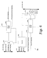
- Fig. 6 provides a block diagram of an example initiator in greater detail to further illustrate the operation of innovative manager 82. More specifically, Fig. 6 illustrates a block diagram of an example PCI initiator 502 in greater detail, according to one embodiment of the present invention.
- PCI initiator 502 comprises a decoder 602, a multiplexer 604, buffers 606 and 608, and a tri-state buffer (610, 612, 614), coupled as depicted.
- clock synchronization boundaries 616 and 618 are depicted with dashed lines. The purpose of the dashed lines are to clearly depict that the clock synchronization boundary is not a physical element of the initiator 502, but rather a logical boundary between a first set of elements that operate at one clock speed and second set of elements that operate at a second clock speed.
- the elements may be a communication bus, or logic coupled to initiator 502 via a communication bus.
- initiator 502 provides a means promoting transactions between elements having disparate communication rates, i.e., between a PCI bus clocking at 33MHz and a FPCI bus clocking at 66MHz.
- an initiator of innovative manager 82 provides a means of traversing clock synchronization boundaries without the need to actually synchronize these interfaces.
- buffer 608 is used to receive transactions from an external PCI bus until an appropriate target indicates that it is ready to process the transaction.
- buffer 608 is referred to as a write buffer.
- buffer 606 is employed to receive data from a target (510, 514, 516) for promotion to an external PCI bus. As will be described more fully below, promoting transaction data from write buffer 608 to an appropriate target, or transferring data received from a target in the read buffer 606 to an external PCI bus requires the assertion of an enable line by decoder 602.
- Decoder 602 is used to decode received transaction identifiers (CallerID) from targets to determine whether the initiator is buffering the identified transaction. If the initiator 502 is buffering transaction data in write buffer 608, denoted by receipt of a unique identifier associated with data in a local buffer, decoder 602 enables the write buffer (608) and an appropriate output 610-614 of tri-state buffer to provide the requesting target with the buffered transaction data. Similarly, to enable a target to issue data to an external PCI data bus, decoder 602 must receive an appropriate identifier to enable the multiplexer 604 to populate read buffer 606 with the data. The data from read buffer 606 is read by a system element via the PCI bus at the clock speed of the PCI bus. The use of the PCI initiator 502 in this way enables an element coupled to manager 82 via a PCI bus clocking at 33MHz to retrieve data residing in NVRAM which is coupled to manager 82 via an interface clocking at 100MHz.
- a flow chart illustrating an example method for concurrently operating on multiple data movement operations begins with step 702 wherein the transaction manager 82 receives a transaction from an external interface (80, 84, 86, 96, 98).
- An initiator (502, 504, 508) associated with the interface, or the data processor 506, receives the transaction and assigns a unique identifier to the transaction.
- the unique identifier is referred to as a CallerID, and may denote the calling initiator as well as the transaction.
- the initiator/data processor (502-508) buffers the transaction in a write buffer (608) and posts the transaction to an appropriate target (510-516) via the transaction bus 518.
- the target is identified by an address, register content, etc.
- an accepting target (510-516) loads the unique identifier in a local transaction queue, step 708.
- the target (510-516) employs a modified FIFO transaction queue wherein transactions are handled in the order in which they are received, with the provision for immediate handling of priority transactions.
- the target When the transaction identifier has reached the top of the queue of the target (510-516), the target will act on the transaction, either requesting transaction data from an appropriate initiator/data processor (502-508), or providing the appropriate initiator with data, step 710. As described above, the actions of the targets 510-516 and the initiators/data processor 502-508 are coordinated via the transaction identifier. Consequently, as described above, when the transaction identifier has reached the top of the transaction queue of a target 510-516, the target issues the transaction identifier on the callback bus 522 to the initiators/data processor 502-508 to denote that the target is now ready to complete the transaction.
- the decoder (602) of the initiators/data processor 502-508 identify that the transaction identifier received from the callback bus 522 is associated with their pending transaction.
- the initiator In response to receiving one of their own transaction identifiers, the initiator either enables the mux 604 to receive data from the target (510-516), or enables an appropriate one of the tri-state buffer (610-614) to supply the target (510-516) with transaction data from write buffer 608 via an appropriate one of data lines 522-528.
- step 712 the target receives/provides the transaction data and the transaction is promoted to a system state.
- each initiator/data processor can simply issue a transaction identifier to a target and buffer the transaction, as it accepts and acts on another transaction. As the target is able to process the transactions, it accesses the requesting initiator/data processor using the transaction identifier. In this way, the initiator(s)/data processor can accommodate transactions at a rate independent of the ability of the target to complete such transactions, limited only by the buffer space available within the initiator/data processor.
- controllers 54a and 54b use the memory map in the mirrored memories 62 and 62b to locate the requested data on the disk array. The data is then stored temporarily in the read cache maintained in the mirrored memories 62a and 62b.
- controller 54a receives a request from the host via I/O module 70a to read data from the disk array.
- the controller CPU 88a processes the request and generates a mirrored read request that involves reading data from the mirrored memories 62a and 62b.
- the mirrored read request is sent to the PCI interface 100 of the AutoRAID memory transaction manager 82a.
- the first controller 54a and its AutoRAID memory transaction manager 82a are referred to as the "local” controller and manager because they receive and originate the mirrored read request.
- the second controller 54b and its AutoRAID memory transaction manager 82b are referred to as the "remote" controller and manager.
- the local and remote managers perform the following steps:
- controller 54a receives a read request that does not require a read compare operation.
- the local controller 54a can read the data from its own memory without requesting the copy from the remote controller.
- the local AutoRAID memory transaction manager performs the following steps:
- the controllers 54a and 54b handle a mirrored write request by (1) storing the data in the write cache maintained in the mirrored memories and (2) updating the memory map in the mirrored memories.
- controller 54a receives a write request to write data to a particular location on the disk array.
- the write request is received at the PCI interface 100 from the PCI bus.
- the local and remote AutoRAID memory transaction managers then perform the following steps:
- the last exemplary transactions involves a situation in which the CPU 88a on the local controller 54a requests a write to a specific memory location and the CPU 88b on the remote controller 54b requests a write to the same memory location.
- the mirrored memory disk array controller is designed to ensure that write requests are ordered and fully completed.
- the dual controllers 54a and 54b assume roles of master/slave or primary/secondary, whereby one controller is crowned with the tasks of ordering transactions and the other controller agrees to abide by this ordering. Determining which controller is the master or primary can be handled ahead of time, as part of a preconfiguration process, or can be negotiated by the controllers when such situations arise.
- the write requests are received at the respective PCI interfaces of the master and slave AutoRAID memory transaction managers 82a and 82b from the PCI bus.
- the master and slave AutoRAID memory transaction managers 82a and 82b then perform the following steps:
- the mirrored read and write transactions described above are handled atomically across the hot-plug interface.
- the controllers are designed to either perform the read and write operations for both NVRAMs, or -to abort performance for both NVRAMs. In this manner, the images presented in the NVRAMs remain identical.
Landscapes
- Engineering & Computer Science (AREA)
- Theoretical Computer Science (AREA)
- Human Computer Interaction (AREA)
- Physics & Mathematics (AREA)
- General Engineering & Computer Science (AREA)
- General Physics & Mathematics (AREA)
- Computer Security & Cryptography (AREA)
- Information Retrieval, Db Structures And Fs Structures Therefor (AREA)
- Bus Control (AREA)
Applications Claiming Priority (2)
| Application Number | Priority Date | Filing Date | Title |
|---|---|---|---|
| US515046 | 2000-02-25 | ||
| US09/515,046 US6801954B1 (en) | 2000-02-25 | 2000-02-25 | Method and apparatus to concurrently operate on multiple data movement transactions in a disk array subsystem |
Publications (2)
| Publication Number | Publication Date |
|---|---|
| EP1128253A2 true EP1128253A2 (fr) | 2001-08-29 |
| EP1128253A3 EP1128253A3 (fr) | 2007-11-07 |
Family
ID=24049756
Family Applications (1)
| Application Number | Title | Priority Date | Filing Date |
|---|---|---|---|
| EP00121113A Withdrawn EP1128253A3 (fr) | 2000-02-25 | 2000-09-28 | Procédé et appareil permettant de traiter simultanément plusieurs opérations de données de transfert dans un sous-système de pile de disques |
Country Status (3)
| Country | Link |
|---|---|
| US (1) | US6801954B1 (fr) |
| EP (1) | EP1128253A3 (fr) |
| JP (1) | JP2001282463A (fr) |
Families Citing this family (8)
| Publication number | Priority date | Publication date | Assignee | Title |
|---|---|---|---|---|
| US7107343B2 (en) * | 2001-07-12 | 2006-09-12 | Adaptec, Inc. | Method and apparatus for improved RAID 1 write performance in low cost systems |
| JP2003030018A (ja) * | 2001-07-13 | 2003-01-31 | Sony Corp | データ通信装置および方法、データ通信システム、情報処理装置および方法、記録媒体、並びにプログラム |
| US7293196B2 (en) * | 2002-05-08 | 2007-11-06 | Xiotech Corporation | Method, apparatus, and system for preserving cache data of redundant storage controllers |
| US7275084B2 (en) * | 2002-05-28 | 2007-09-25 | Sun Microsystems, Inc. | Method, system, and program for managing access to a device |
| US7453888B2 (en) * | 2002-08-27 | 2008-11-18 | Alcatel Lucent | Stackable virtual local area network provisioning in bridged networks |
| US20040111537A1 (en) * | 2002-12-05 | 2004-06-10 | Intel Corporation | Method, system, and program for processing operations |
| US20100229029A1 (en) * | 2009-03-06 | 2010-09-09 | Frazier Ii Robert Claude | Independent and dynamic checkpointing system and method |
| US20130304970A1 (en) * | 2012-04-20 | 2013-11-14 | Stec, Inc. | Systems and methods for providing high performance redundant array of independent disks in a solid-state device |
Family Cites Families (17)
| Publication number | Priority date | Publication date | Assignee | Title |
|---|---|---|---|---|
| US5392244A (en) | 1993-08-19 | 1995-02-21 | Hewlett-Packard Company | Memory systems with data storage redundancy management |
| EP0717358B1 (fr) | 1994-12-15 | 2001-10-10 | Hewlett-Packard Company, A Delaware Corporation | Système de détection de défaut pour une mémoire miroir dans un contrôleur dupliqué d'un système de mémoire disques |
| US5638531A (en) * | 1995-06-07 | 1997-06-10 | International Business Machines Corporation | Multiprocessor integrated circuit with video refresh logic employing instruction/data caching and associated timing synchronization |
| US6108735A (en) * | 1995-09-29 | 2000-08-22 | Intel Corporation | Method and apparatus for responding to unclaimed bus transactions |
| US5812803A (en) * | 1995-09-29 | 1998-09-22 | Intel Corporation | Method and apparatus for controlling data transfers between a bus and a memory device using a multi-chip memory controller |
| US5687390A (en) * | 1995-11-14 | 1997-11-11 | Eccs, Inc. | Hierarchical queues within a storage array (RAID) controller |
| US5787304A (en) * | 1996-02-05 | 1998-07-28 | International Business Machines Corporation | Multipath I/O storage systems with multipath I/O request mechanisms |
| US5983326A (en) * | 1996-07-01 | 1999-11-09 | Sun Microsystems, Inc. | Multiprocessing system including an enhanced blocking mechanism for read-to-share-transactions in a NUMA mode |
| US6260096B1 (en) * | 1999-01-08 | 2001-07-10 | Intel Corporation | Read latency across a bridge |
| US6134630A (en) * | 1997-11-14 | 2000-10-17 | 3Ware | High-performance bus architecture for disk array system |
| US6298407B1 (en) * | 1998-03-04 | 2001-10-02 | Intel Corporation | Trigger points for performance optimization in bus-to-bus bridges |
| US6425041B1 (en) * | 1998-06-05 | 2002-07-23 | Micron Technology, Inc. | Time-multiplexed multi-speed bus |
| US6230240B1 (en) * | 1998-06-23 | 2001-05-08 | Hewlett-Packard Company | Storage management system and auto-RAID transaction manager for coherent memory map across hot plug interface |
| US6240479B1 (en) * | 1998-07-31 | 2001-05-29 | Motorola, Inc. | Method and apparatus for transferring data on a split bus in a data processing system |
| US6122723A (en) * | 1998-08-20 | 2000-09-19 | International Business Machines Corporation | Switching multi-initiator SCSI devices to a singular target bus |
| US6418518B1 (en) * | 1998-09-18 | 2002-07-09 | National Semiconductor Corporation | Decoupled address and data access to an SDRAM |
| TW514788B (en) * | 1999-04-23 | 2002-12-21 | Via Tech Inc | Method of delayed transaction in bus system and device using the method |
-
2000
- 2000-02-25 US US09/515,046 patent/US6801954B1/en not_active Expired - Lifetime
- 2000-09-28 EP EP00121113A patent/EP1128253A3/fr not_active Withdrawn
-
2001
- 2001-02-23 JP JP2001048235A patent/JP2001282463A/ja not_active Withdrawn
Also Published As
| Publication number | Publication date |
|---|---|
| US6801954B1 (en) | 2004-10-05 |
| JP2001282463A (ja) | 2001-10-12 |
| EP1128253A3 (fr) | 2007-11-07 |
Similar Documents
| Publication | Publication Date | Title |
|---|---|---|
| US6230240B1 (en) | Storage management system and auto-RAID transaction manager for coherent memory map across hot plug interface | |
| US6772310B2 (en) | Method and apparatus for zeroing a transfer buffer memory as a background task | |
| US6330642B1 (en) | Three interconnected raid disk controller data processing system architecture | |
| US7093043B2 (en) | Data array having redundancy messaging between array controllers over the host bus | |
| US7373438B1 (en) | System and method for reprioritizing high-latency input/output operations | |
| US5586291A (en) | Disk controller with volatile and non-volatile cache memories | |
| US5802345A (en) | Computer system with a reduced number of command end interrupts from auxiliary memory unit and method of reducing the number of command end interrupts | |
| Katz | High-performance network and channel-based storage | |
| US5875479A (en) | Method and means for making a dual volume level copy in a DASD storage subsystem subject to updating during the copy interval | |
| EP0768599B1 (fr) | Reconfiguration en ligne d'un réseau de disques | |
| US6505273B2 (en) | Disk control device and method processing variable-block and fixed-block accesses from host devices | |
| JP3364572B2 (ja) | 多重パスi/o要求機構を有するデータ処理システム及びキュー・ステータス更新方法 | |
| JP4817783B2 (ja) | Raidシステム及びそのリビルド/コピーバック処理方法 | |
| US5978856A (en) | System and method for reducing latency in layered device driver architectures | |
| US6728791B1 (en) | RAID 1 read mirroring method for host adapters | |
| US20020124138A1 (en) | Internal copy for a storage controller | |
| US20040186931A1 (en) | Transferring data using direct memory access | |
| JPH07504527A (ja) | 高性能の不揮発性ram保護式の書き込みキャッシュアクセラレータシステム | |
| JPH10105344A (ja) | データ記録装置システム及びそのデータ書込方法 | |
| JP4536361B2 (ja) | データ転送装置、記憶デバイス制御装置、記憶デバイス制御装置の制御方法 | |
| JP2003029934A (ja) | ストレージ制御装置及びその制御方法 | |
| US6801954B1 (en) | Method and apparatus to concurrently operate on multiple data movement transactions in a disk array subsystem | |
| JP2807010B2 (ja) | ホストコンピュータとテープ駆動部間の相互接続用のテープ駆動制御ユニットおよびその操作方法 | |
| US6701385B1 (en) | Raid 1 write mirroring method for host adapters | |
| JPH06119123A (ja) | ディスクアレイ装置 |
Legal Events
| Date | Code | Title | Description |
|---|---|---|---|
| PUAI | Public reference made under article 153(3) epc to a published international application that has entered the european phase |
Free format text: ORIGINAL CODE: 0009012 |
|
| AK | Designated contracting states |
Kind code of ref document: A2 Designated state(s): AT BE CH CY DE DK ES FI FR GB GR IE IT LI LU MC NL PT SE |
|
| AX | Request for extension of the european patent |
Free format text: AL;LT;LV;MK;RO;SI |
|
| PUAL | Search report despatched |
Free format text: ORIGINAL CODE: 0009013 |
|
| AK | Designated contracting states |
Kind code of ref document: A3 Designated state(s): AT BE CH CY DE DK ES FI FR GB GR IE IT LI LU MC NL PT SE |
|
| AX | Request for extension of the european patent |
Extension state: AL LT LV MK RO SI |
|
| 17P | Request for examination filed |
Effective date: 20080320 |
|
| AKX | Designation fees paid |
Designated state(s): DE FR GB |
|
| STAA | Information on the status of an ep patent application or granted ep patent |
Free format text: STATUS: THE APPLICATION IS DEEMED TO BE WITHDRAWN |
|
| 18D | Application deemed to be withdrawn |
Effective date: 20090401 |