EP1128262A2 - Circuit de mappage et procédé pour changer la désignation de registres - Google Patents
Circuit de mappage et procédé pour changer la désignation de registres Download PDFInfo
- Publication number
- EP1128262A2 EP1128262A2 EP01301251A EP01301251A EP1128262A2 EP 1128262 A2 EP1128262 A2 EP 1128262A2 EP 01301251 A EP01301251 A EP 01301251A EP 01301251 A EP01301251 A EP 01301251A EP 1128262 A2 EP1128262 A2 EP 1128262A2
- Authority
- EP
- European Patent Office
- Prior art keywords
- value
- range
- output
- values
- input
- Prior art date
- Legal status (The legal status is an assumption and is not a legal conclusion. Google has not performed a legal analysis and makes no representation as to the accuracy of the status listed.)
- Withdrawn
Links
Images


Classifications
-
- G—PHYSICS
- G06—COMPUTING OR CALCULATING; COUNTING
- G06F—ELECTRIC DIGITAL DATA PROCESSING
- G06F8/00—Arrangements for software engineering
- G06F8/40—Transformation of program code
- G06F8/41—Compilation
- G06F8/44—Encoding
- G06F8/445—Exploiting fine grain parallelism, i.e. parallelism at instruction level
- G06F8/4452—Software pipelining
-
- G—PHYSICS
- G06—COMPUTING OR CALCULATING; COUNTING
- G06F—ELECTRIC DIGITAL DATA PROCESSING
- G06F9/00—Arrangements for program control, e.g. control units
- G06F9/06—Arrangements for program control, e.g. control units using stored programs, i.e. using an internal store of processing equipment to receive or retain programs
- G06F9/30—Arrangements for executing machine instructions, e.g. instruction decode
- G06F9/32—Address formation of the next instruction, e.g. by incrementing the instruction counter
- G06F9/322—Address formation of the next instruction, e.g. by incrementing the instruction counter for non-sequential address
- G06F9/325—Address formation of the next instruction, e.g. by incrementing the instruction counter for non-sequential address for loops, e.g. loop detection or loop counter
-
- G—PHYSICS
- G06—COMPUTING OR CALCULATING; COUNTING
- G06F—ELECTRIC DIGITAL DATA PROCESSING
- G06F9/00—Arrangements for program control, e.g. control units
- G06F9/06—Arrangements for program control, e.g. control units using stored programs, i.e. using an internal store of processing equipment to receive or retain programs
- G06F9/30—Arrangements for executing machine instructions, e.g. instruction decode
- G06F9/38—Concurrent instruction execution, e.g. pipeline or look ahead
- G06F9/3836—Instruction issuing, e.g. dynamic instruction scheduling or out of order instruction execution
- G06F9/3838—Dependency mechanisms, e.g. register scoreboarding
- G06F9/384—Register renaming
Definitions
- the present invention relates to circuitry and a method for performing a fast mapping from an input value to an output value.
- the present invention can be applied to register renaming in pipelined loops in a microprocessor.
- a processor may include a plurality of individual execution units, with each individual unit being capable of executing one or more instructions in parallel with the execution of instructions by the other execution units.
- Such a plurality of execution units can be used to provide a so-called software pipeline made up of a plurality of individual stages.
- Each software pipeline stage has no fixed physical correspondence to particular execution units. Rather, when a loop structure in an application program is compiled the machine instructions which make up an individual iteration of the loop are scheduled for execution by the different execution units in accordance with a software pipeline schedule. This schedule is divided up into successive stages and the instructions are scheduled in such a way as to permit a plurality of iterations to be carried out in overlapping manner by the different execution units with a selected loop initiation interval between the initiations of successive iterations.
- the name of a value held in a register is known to the programmer or compiler in terms of the register identifiers within each assembly-code instruction.
- the purpose of static register renaming is to define a scheme whereby these identifiers are translated at run-time into actual register numbers based on a translation scheme that can be predicted by the programmer or compiler.
- each loop-variant value is assigned a logical register number within the rotating register file, and this logical register number does not change from one iteration to the next.
- each logical register number is mapped to a physical register within the register file and this mapping is rotated each time a new iteration is begun, i.e. each time a pipeline boundary is closed.
- corresponding instructions in different iterations can all refer to the same logical register number, making the compiled instructions simple, whilst avoiding a value produced by one iteration from being overwritten by a subsequently-executed instruction of a different iteration.
- mapping circuitry for mapping an input value, within a preselected range of allowable input values, to a corresponding output value within a preselected range of allowable output values, said circuitry comprising: first candidate output value producing means connected for receiving said input value and operable to produce a first candidate output value that differs by a first offset value from the received input value; second candidate output value producing means connected for receiving said input value and operable, during operation of said first candidate output value producing means to produce said first candidate output value, to produce a second candidate output value that differs by a second offset value from the received input value, the first and second offset values being such that a difference between them is equal to a difference between respective output-range limit values defining the limits of the preselected output-value range and such that, for any said input value within the said preselected input-value range, one of the first and second candidate output values is within the preselected output-value range and the other of those two values is outside that range; in-range value determining means for
- mapping circuitry for mapping an input value, within a preselected range of allowable input values, to a corresponding output value within a preselected range of allowable output values, said circuitry comprising: first candidate output value producing means connected for receiving said input value and operable to produce a first candidate output value that differs by a first offset value from the received input value; second candidate output value producing means connected for receiving said input value and operable to produce a second candidate output value that differs by a second offset value from the received input value, the first and second offset values being such that a difference between them is equal to a difference between respective output-range limit values defining the limits of the preselected output-value range and such that, for any said input value within the said preselected input-value range, one of the first and second candidate output values is within the preselected output-value range and the other of those two values is outside that range; in-range value determining means operable to determine, during operation of one or both of said first and second candidate value producing means
- a mapping method for mapping an input value, within a preselected range of allowable input values, to a corresponding output value within a preselected range of allowable output values, said method comprising the steps of: producing a first candidate output value that differs by a first offset value from the received input value; producing, during production of said first candidate output value, a second candidate output value that differs by a second offset value from the received input value, the first and second offset values being such that a difference between them is equal to a difference between respective output-range limit values defining the limits of the preselected output-value range and such that, for any said input value within the said preselected input-value range, one of the first and second candidate output values is within the preselected output-value range and the other of those two values is outside that range; determining which one of said first and second candidate output values is within said preselected output-value range; and selecting as said corresponding output value that one of said first and second candidate output values which is determined to be
- a mapping method for mapping an input value, within a preselected range of allowable input values, to a corresponding output value within a preselected range of allowable output values, said method comprising the steps of: producing a first candidate output value that differs by a first offset value from the received input value; producing a second candidate output value that differs by a second offset value from the received input value, the first and second offset values being such that a difference between them is equal to a difference between respective output-range limit values defining the limits of the preselected output-value range and such that, for any said input value within the said preselected input-value range, one of the first and second candidate output values is within the preselected output-value range and the other of those two values is outside that range; determining, during production of one or both of said first and second candidate output values, which one of said first and second candidate output values is within said preselected output-value range; and selecting as said corresponding output value that one of said first and second candidate output
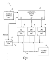
- Fig. 1 shows parts of a processor to which an embodiment of the present invention is applicable.
- the processor is a very long instruction word (VLIW) processor with hardware support for software pipelining and cyclic register renaming.
- the processor 1 includes an instruction issuing unit 10, a schedule storage unit 12, respective first, second and third execution units 14, 16 and 18, and a register file 20.
- the instruction issuing unit 10 has three issues slots IS1, IS2 and IS3 connected respectively to the first, second and third execution units 14, 16 and 18.
- a first bus 22 connects all three execution units 14, 16 and 18 to the register file 20.
- a second bus 24 connects the first and second units 14 and 16 (but not the third execution unit 18 in this example) to a memory 26 which, in this example, is an external random access memory (RAM) device.
- the memory 26 could alternatively be a RAM internal to the processor 1.
- FIG. 1 shows shared buses 22 and 24 connecting the execution units to the register file 20 and memory 26, it will be appreciated that alternatively each execution unit could have its own independent connection to the register file and memory.
- the processor 1 performs a series of processing cycles.
- the instruction issuing unit 10 can issue one instruction at each of the issue slots IS1 to IS3.
- the instructions are issued according to a software pipeline schedule (described below) stored in the schedule storage unit 12.
- the instructions issued by the instructing issuing unit 10 at the different issue slots are executed by the corresponding execution units 14, 16 and 18.
- each of the execution units can execute more than one instruction at the same time, so that execution of a new instruction can be initiated prior to completion of execution of a previous instruction issued to the execution unit concerned.
- each execution unit 14, 16 and 18 has access to the register file 20 via the first bus 22. Values held in registers contained in the register file 20 can therefore be read and written by the execution units 14, 16 and 18. Also, the first and second execution units 14 and 16 have access via the second bus 24 to the external memory 26 so as to enable values stored in memory locations of the external memory 26 to be read and written as well. The third execution unit 18 does not have access to the external memory 26 and so can only manipulate values contained in the register file 20 in this example.
- VLIW very long instruction word
- the symbolic data-flow graph shows how data, and operators which act upon that data, are utilized during the loop, and is useful for highlighting the time-dependencies within a loop and for determining any time optimizations which can be made to increase the time efficiency of a loop.
- the "add" operation in node D5 first requires the value of dy(i) to be accessed (node D4) and the values of da and dx(i) to be accessed (nodes D1 and D2 respectively) and multiplied (node D3). It is apparent that the operations (D1, D2, D3) can be performed at the same time, or overlapping with, the operation D4 such that any values required for operation D5 are ready for use by the start of that operation.
- the result of the "add" operation in node D5 is subsequently stored in dy(i) in node D5.
- Nodes D7 to D9 implement the incrementing of the array variable "i" at the end of every iteration.
- each array dx and dy will be stored in memory locations in the external memory 26 (Fig. 1) and so references to them in the Fig. 1 data-flow graph must be converted into corresponding memory access operations.
- each array dx and dy needs at least one pointer for pointing to the storage locations in the external memory 26 where the elements of the array are stored.
- Each such pointer is held in a register of the register file 20.
- the constant value da could be dealt with using a similar pointer to its location in the memory, as the value is loop-invariant it is more convenient and fast to keep it directly in its own register of the register file 20 during execution of the loop.
- the next step in the process of compiling the example loop shown in the code box above would be to perform a variety of optimisations to convert the data-flow graph shown in Fig. 2 into a form which is closer to actual machine instructions.
- the compiler would typically determine what values change within the loop and what values remain the same. For example, in this case, the value of "da" is not altered at all during the loop.
- Array references are converted into pointer accesses, and auto-increment addressing modes are used if the target machine supports such a feature.
- the resulting internal tree-structured compiler representation is illustrated in Fig. 3.
- the illustrated representation shows the individual machine operations T1 to T6, their dependence relationships (as arrows) and attached to each arrow is an integer which represents the number of processor cycles required to complete the operation from which the arrow points. Use is made of registers r0 to r3, as well as virtual registers v0 to v3.
- Instructions T1 to T6 illustrated in Fig. 3 relate closely to corresponding nodes D1 to D6 of the symbolic data-flow graph illustrated in Fig. 2. Intermediate values are assigned virtual register numbers v0 to v3, whilst other values are assigned register numbers r1 to r3.
- the virtual register numbers are not the final register assignments but are merely temporary labels for the arrows in the data-flow graph illustrated in Fig. 2 (as will be explained in more detail below).
- the longest path between any pair of instructions defines the minimum amount of time required to execute one iteration of the loop. This is known as the "schedule length" and is formally defined as the sum of the latencies along the longest (critical) path plus 1. In this example, therefore, the schedule length is ten cycles. A register which is auto-incremented in one cycle is ready for use again in the next cycle.
- the first phase of software pipelining is to determine the loop initiation interval (referred to simply as "II"), which is the interval between initiation of successive iterations of the loop.
- II loop initiation interval
- the loop initiation interval depends on the available resources in comparison with the number of instructions to execute, as well as the presence of any cycles in the data-flow graph.
- the Fig. 1 processor has three instruction issue slots IS1 to IS3 and three execution units 14, 16 and 18, of which only the first and second execution units 14 and 16 are capable of accessing the external memory 26.
- the execution units may be "specialised" units in the sense that they are optimised individually for carrying out different tasks. For example, it may be that only certain of the execution units are capable of performing certain types of instruction.
- the loop initiation interval II is determined as two processor cycles. Also, it will be assumed that only the third execution unit 18 is equipped with the resources (e.g. an arithmetic and logic unit ALU) necessary to execute add and multiply instructions.
- resources e.g. an arithmetic and logic unit ALU
- the next step is to create a schedule which obeys a so-called modulo scheduling constraint.
- An example schedule is shown in Fig. 4.
- the first issue slot handles only "ld” instructions
- the second issue slot handles only "st” instructions
- the third issue slot handles the arithmetic operators "mul" and "add”.
- the modulo scheduling constraint specifies that, for each issue slot, an instruction can be scheduled at time i if and only if there are no instructions scheduled at time j such that j modulo II is equal to i. This ensures that, with a new iteration starting every II cycles, there is no possibility that more than one instruction is required to be issued in a particular cycle of a particular issue slot.
- the modulo scheduling table shows how the five instructions T2 to T6 making up one iteration of the loop are scheduled.
- columns 3 to 5 of the table show the cycle in the schedule when each instruction is issued, the software pipeline stage in which it occurs, and the issue slot by which the instruction is issued (i.e. the execution unit which executes the instruction).
- the final four columns indicate logical register numbers and shading is used to illustrate value lifetimes, as will be explained later in detail with reference to Figs. 6 to 8.
- the schedule in the Fig. 4 table relates to one iteration only. Every II cycles another iteration is initiated according to the same schedule. Thus, when the current iteration is at stage 1, the immediately-preceding iteration will be at stage 2, the iteration before that will be at stage 3, the iteration before that at stage 4 and the iteration before that at stage 5.
- the instructions are scheduled for issue by the same issue slots in all iterations, that each issue slot issues the same instruction every II cycles.
- s0, s1, s2 up to sr may be allocated in place of the virtual registers as shown in the four right-most columns. It is apparent from Fig. 4 that the register allocated to v0 changes from being s0 in stage 1 to s1 in stage 2. This is because the renaming mechanism effectively shifts the register names by one each time a pipeline boundary is crossed and a new iteration is begun. This allows the value of v0 computed in iteration i to be distinguished from the value of v0 computed in iterations i+1 and i-1.
- registers s0 to sr are therefore not the final physical register numbers, but are logical register numbers which are converted (mapped) at run-time to physical register numbers.
- a loop-invariant value is a value which is used inside the loop, but which is never re-computed within the loop.
- An example is the value "da" in the above example loop.
- Such values must be stored in registers that do not undergo register renaming during loop execution.
- the pointers to the arrays dx and dy, although not loop-invariant values, can also be stored in statically-named registers in this example. Consequently, a register file for use in this context will require a renamable portion for holding loop-variant values, and a statically-named portion for holding loop-invariant values and other suitable values.
- FIG. 5 One example of such a register file is illustrated in Fig. 5.
- the example register file 120 shown in Fig. 5 consists of N registers. Of these, the lower-numbered K are statically named and the higher-numbered N-K are dynamically named (renamable).
- the statically-named registers make up a statically-named portion 120S of the register file and the renamable registers make up a renamable portion 120R of the register file.
- the Fig. 5 register file requires mapping circuitry that implements a bijective mapping from logical register identifiers (numbers) to physical register identifiers (addresses).
- Each physical register address P is also an m-bit binary integer in the range 0 to N-1, and identifies directly one of the actual hardware registers.
- OFFSET is a mapping offset value (integer) which increases (or decreases) monotonically by one whenever the registers are renamed.
- FIG. 6B The table of Fig. 6B is a continuation of the table shown in Fig. 6A.
- the table shows the register renaming scheme in operation for the same example as described above, with the first two iterations illustrated in Fig. 6A and the next two iterations illustrated in Fig. 6B.
- the value of K is assumed to be equal to four (since there are four statically-named registers r0 to r3).
- the value of N is assumed to be sufficiently large that it does not affect the progress of the present example.
- the mapping offset value OFFSET is initialised to the value 6, and is made to decrease by one every time a pipeline boundary is crossed, as shown in the second column of Figs. 6A and 6B.
- the sequence of instructions shown in the first column of iteration 0 of Fig. 6A is the same as the sequence of instructions shown divided into three columns (issue slots 1 to 3) in Fig. 4.
- the statically-named registers are assigned logical register numbers r0 to r3.
- the loop-variant registers are given temporary labels v0 to v3. The same set of temporary labels are used for each iteration, so that the first column of each iteration shows the same sequence of instructions, shifted by the iteration interval II (which in this case is two cycles).
- the temporary virtual register numbers v0 to v3 are converted into logical register numbers, as shown in the corresponding columns headed v0 to v3 within each iteration illustrated in Figs. 6A and 6B.
- the virtual register number v0 in cycles 0 and 1 of iteration 0 is assigned, by the compiler, the logical register number r4.
- this logical register number is converted to a physical register number by using equation (1) above to map from R to P.
- logical register number r4 is mapped at run-time to physical register number p10 in this example.
- the compiler When a pipeline boundary is crossed, in order to identify the same register after the boundary is crossed the compiler must use a logical register number that is incremented by one compared to the logical register number used before the crossing, so that at run-time, when the mapping is also rotated at each pipeline boundary, the correct physical register will be accessed from one stage to another. For example, considering the virtual register number v0 in iteration 0, when the pipeline boundary is crossed going from cycle 1 to cycle 2, the logical register number is incremented from r4 to r5, so that the same physical register number (p10) is accessed in the second stage, taking into account the fact that OFFSET has decreased to 5.
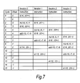
- Fig. 7 shows the result of the allocation of logical register numbers by the compiler for the sequence of instructions for each of the iterations 0 to 3 shown in Figs. 6A and 6B.
- Fig. 8 shows the effect of the register mapping which is performed at run-time to map the logical register numbers to physical register numbers.
- mapping equation (1) for the mapping from logical register number R to physical register P, when renaming the rotating registers OFFSET may be incremented or it may be decremented. If it is incremented then the logical register number of a particular physical register decreases by one each time OFFSET is incremented. Likewise if OFFSET is decremented the logical register numbers increase.
- Fig. 9 The mapping from logical register identifiers to physical register identifiers is illustrated graphically in Fig. 9.
- Fig. 9 There is a direct mapping of logical register numbers in the range 0 to l s -1 to physical register numbers in the statically-named space from 0 to K-1, and consequently K ⁇ l s .
- the renamable space may be set apart from the statically-named space by setting K > l s .
- Logical register numbers in the range l s to l e map to a region of equal size in the renamable space between K and N-1. The location of this region within the renamable space is varied in accordance with the mapping offset values OFFSET.
- the evaluation of P in the mapping equation (1) is performed at run-time and is a time-critical activity within the pipeline of a high-performance processor as it requires a number of integer calculations before each required register can be accessed.
- mapping equation (1) involves a time-consuming modulus operation.
- Mapping circuitry embodying the present invention is intended to realise a faster implementation of the mapping from logical register numbers to physical register numbers, in particular by avoiding the need for the calculation of a modulus operation.
- Fig. 10 shows parts of mapping circuitry embodying the present invention.
- the mapping circuitry 40 includes respective first and second candidate output value producing units 42 and 44, an in-range value determining unit 46 and an output value selecting unit 48.
- a third candidate output value producing unit 50 may also be provided.
- the first and second candidate output value producing units 42 and 44 are each connected for receiving an input value r.
- the first candidate output value producing unit 42 produces a first candidate output value C1 that differs by a first offset value x from the received input value r.
- the second candidate output value producing unit 44 produces a second candidate output value C2 that differs by a second offset value y from the received input value r.
- a difference y-x between the first and second offset values is equal to a difference between respective output-range limit values K and N defining the limits of a preselected range of allowable output values p (e.g. from K to N-1) of the mapping circuitry.
- the first and second offset values x and y are such that, for any input value within a preselected range of allowable input values (l s ⁇ r ⁇ l e ), one of the first and second candidate output values C1 and C2 is within the preselected output-value range (K to N-1) and the other of those two values C1 and C2 is outside that range.
- the in-range value determining unit 46 determines which one of the first and second candidate output values C1 and C2 is within the preselected output-value range.
- the output value selecting unit 48 selects as the output value p corresponding to the received input value r that one of the first and second candidate output values C1 and C2 which is determined to be within the output-value range.
- the in-range value determining unit 46 applies a selection signal S to the output value selecting unit 48 to indicate the selection to be made by that unit.
- the second candidate output value producing unit 44 operates to produce the second candidate output value C2. This enables the first and second candidate output values C1 and C2 to be available for selection by the output value selecting unit 48 more quickly than if the values were produced sequentially, for example by a single candidate output value producing unit.
- the in-range value determining unit 46 may examine the produced candidate output values C1 and C2 directly to determine which one of them is in-range.
- the in-range value determining unit 46 operates to determine which one of those candidate output values C1 and C2 will be in-range.
- the in-range value determining unit 46 may be connected for receiving the input value r.
- the in-range value determining unit 46 may also make use of an in-range offset value w which has a known relationship with (e.g. a fixed difference from) each of the first and second offset values x and y.
- This in-range offset value w is employed with the input value r to make the in-range determination independently of the candidate output values C1 and C2 as produced by the candidate output value producing units 42 and 44.
- all or part of the selection signal S may be derived by combining the in-range offset value w with the input value r.
- the in-range value determining unit 46 operates during operation of one or both of the first and second candidate output value producing units 42 and 44, the in-range determination does not have to be deferred until the candidate output values C1 and C2 are actually produced by those units.
- the first and second candidate output value producing units 42 and 44 do not have to operate at the same time in the second aspect of the invention.
- the first and second candidate output value producing units 42 and 44 and the in-range value determining unit 46 all operate at the same time so that the selection of the in-range candidate output value C1 or C2 can take place as soon as the candidate output values C1 and C2 are produced by the units 42 and 44.
- the optional third candidate output value producing unit 50 produces a third candidate output value C3 which may or may not be dependent on the input value r.
- the third candidate output value C3 may simply be set equal to the input value r.
- the value C3 is preferably produced by the unit 50 during operation of one or more of the units 42, 44 and 46.
- Fig. 11 is a flowchart for use in explaining a method for mapping an input value (logical register number) to a corresponding output value (physical register number) in a preferred embodiment of the present invention.
- this method three initialisation values I x , I y and I w are used, as follows:
- steps S1, S2 and S3 are set in steps S1, S2 and S3 respectively in Fig. 11.
- steps S4, S5 and S6 three count values x, y and w are set to the initialisation values I x , I y and I w respectively.
- the count value x represents the first offset value
- the count value y represents the second offset value
- the count value w represents the in-range offset value.
- the settings performed in steps S4 to S6 are repeated occasionally and are referred to collectively as a "reset" operation.
- step S7 a new input value r is received.
- step S8 the value of I w + r is examined. If it is less than 0 (i.e. r ⁇ l s ) then the output value p is set to r (third candidate output value C3) in step S9, and processing then jumps to step S13. If in step S8 I w + r ⁇ 0 (i.e. r ⁇ l s ) then the value of w + r is examined in step S10.
- step S10 If the value of w + r is less than 0 then the output value p is set to y + r (second candidate output value C2) in step S11 and processing jumps to step S13. If in step S10 w + r ⁇ 0 then the output value p is set to x + r (first candidate output value C1) in step S12 and processing is continued with step S13. In step S13 the computed output value p is output.
- step S14 it is determined whether the register mapping is to be rotated. This would happen, for example, when a pipeline boundary is encountered and a new iteration is begun. If the register mapping is not to be rotated, then processing returns to step S7 to receive a new input value r to be mapped as before.
- the results can be used to select the appropriate one of the results of steps S9 (C3), S11 (C2) and S12 (C1) as the output value p to be output in step S13.
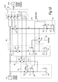
- Fig. 12 shows, in register transfer level (RTL) representation, one example of register mapping circuitry according to a preferred embodiment of the present invention.
- the Fig. 12 circuitry 60 is intended to perform the method illustrated in Fig. 11, and in Fig. 12 the reference numerals H4 to H13 assigned to the elements of the mapping circuitry are intended to assist in an understanding of the correspondence between those elements and the steps S4 to S13 in Fig. 11.
- the mapping circuitry 60 has an input H7 for receiving an m-bit input value (logical register number) r and an output H13 for outputting an m-bit output value (mapped physical register number) p corresponding to the input value r.
- m 5 or 6.
- the circuitry also contains four adders H8, H10, H11 and H12, three registers H1, H2 and H3, three counters H4, H5 and H6, a comparator H15 and a multiplexer H100.
- the adder H12, the counter H4 and the register H1 together correspond to the first candidate output value producing unit 42 in Fig. 8.
- the adder H11, the counter H5 and the register H2 together correspond to the second candidate output value producing unit 44.
- the adder H10, the counter H6 and the register H3 together correspond to the in-range determining unit 46.
- the multiplexer H100 corresponds to the output value selecting unit 48.
- the adder H8 is included in an input range determining unit 62 and the comparator H15 is included in an offset varying unit 64.
- Each of the adders H8, H10, H11 and H12 has a first and second inputs.
- the respective first inputs of all four adders are connected directly to the input H7 for receiving therefrom the m-bit logical register number r.
- the second input of the adder H8 is connected to an output of the register H3.
- the second input of the adder H10 is connected to an output of the counter H6.
- the second input of the adder H11 is connected to an output of the counter H5.
- the second input of the adder H12 is connected to an output of the counter H4.
- the multiplexer H100 has four m-bit inputs, two of which are connected directly to the input H7 for receiving the m-bit input value r (third candidate output value C3).
- the other two m-bit inputs to the multiplexer H100 are connected to respective outputs of the adders H11 (second candidate output value C2) and H12 (first candidate output value C1).
- the multiplexer H100 also has a selection input for receiving a two-bit selection signal S [s1, s0].
- the bit s1 of the selection signal S is the most significant bit (bit m) of the output of adder H8.
- the bit s0 of the selection signal S is the most significant bit (bit m) of the output of the adder H10.
- the comparator H15 has a first input connected to an output of the register H1 and a second input connected to an output of the counter H5.
- the offset varying unit 64 has an input connected for receiving a RENAME signal.
- the offset varying unit 64 also has an output connected to respective inputs of the counters H4 to H6 for applying selectively thereto either a reset signal RESET or a decrement signal DEC.
- the register H1 has an output connected to an input of the counter H4, the register H2 has an output connected to an input of the counter H5, and the register H3 has an output connected to an input of the counter H6.
- the registers H1, H2 and H3 are used for storing the above-mentioned initialisation values I x , I y and I w respectively.
- the counters H4, H5 and H6 are used for holding the above-mentioned count values x, y and w respectively.
- the registers H1, H2 and H3 are initialised respectively with the values I x , I y and I w (the control logic for initialising these registers has been omitted from Fig. 2 for clarity).
- the offset varying unit 64 applies the RESET signal to the counters H4, H5 and H6 so that they are loaded respectively with the values of I x , I y and I w in steps S4, S5 and S6 (the above-mentioned "reset" operation).
- the most significant bit (s1 for adder H8 and s0 for adder H10) of the detection value D1 or D2 indicates by itself whether that value is less than zero. If the detection value is less than zero, then the most significant bit is high (1); otherwise it is low (0).
- the two bits s0 and s1 make up the selection signal S used to select one of the four inputs of the multiplexer H100.
- the first candidate output value (input "00") is the value x+r produced by the adder H12.
- the second candidate output value (input "01”) is the value y+r produced by the adder H11.
- the third candidate output value (inputs "10” and "11") is the r-value received at the input H7.
- this value is selected as the output of the multiplexer H100 whenever the selection bit s1 is 1 (this indicates that the result D1 of the addition carried out by adder H8 is negative). This corresponds to the determination "YES” in step S8 of Fig. 11 (I w +r ⁇ 0), and the output physical register number p being set equal to the input logical register number r in step S9.
- step S8 the second candidate output value C2 is selected as the output of the multiplexer H100, corresponding to a determination "NO” in step S8 (I w +r ⁇ 0) and a determination "YES” in step S10 (w+r ⁇ 0).
- the first candidate output value C1 is selected as the output of the multiplexer H100, corresponding to a determination "NO” in step S8 (I w +r ⁇ 0) and a determination "NO” in step S10 (w+r ⁇ 0).
- a rotation operation, for rotating the register mapping, is carried out in the Fig. 12 circuitry by the offset varying unit 64 in response to receipt of the control signal RENAME.
- the offset varying unit 64 produces the decrement control signal DEC.
- the values stored in registers H4, H5 and H6 are each decremented by one in response to the DEC signal, corresponding to steps S16, S17 and S18. In this way, the first, second and in-range offset values x, y and w are varied within the appropriate ranges whilst always maintaining the same differences between them.
- the addition operation required to produce the first candidate output value x+r is carried out by the adder H12 at the same time as the addition operation required to produce the second candidate output value y+r is carried out by the adder H11.
- the adder H12 For any given r-value in the range from l s to l e (allowable input-value range for mapping to the renamable space in the register file), one of the first and second candidate output values will be in the range from K to N-1 of allowable output values (physical register numbers in the renamable space) and the other candidate output value will be outside the range.
- the third addition operation w+r used to produce the detection value D2 in this embodiment is independent of the operations to produce the first and second candidate output values. This third addition operation is therefore carried out at the same time as those operations. This means that the determination of the in-range candidate output value is not delayed until those two candidate values have been produced.
- the received r-value (third candidate output value C3) is also selected when r ⁇ l s .
- the fourth addition operation I w +r used to produce the detection value D1 in this embodiment is independent of the operations to produce the first and second candidate output values and of the operation to determine the in-range one of those values.
- the fourth addition operation is therefore carried out at the same time as those other operations. This means that the production of the first and second candidate output values is not delayed by the operation to determine whether to select the third candidate output value, or vice versa.
- the Fig. 12 implementation therefore uses four parallel adders and a 4-to-1 multiplexer to compute the output value r.
- the resulting logic requires only the amount of time necessary to complete the addition of two (m+1)-bit integers, and the time to select one of the four m-bit values. Therefore the critical path through the logic for computing the physical register number p corresponding to a logical register number r is one (short) integer addition and 1-of-4 selection. This represents a considerable time saving in comparison to the computation of a modulus operation.
- the complete state of the register mapping is contained within the counters and registers H1 to H6 (offset values x, y, w and the initialisation values I x , I y and I w ).
- the mapping circuitry 60 is incorporated within a processor such as the Fig. 1 processor, therefore, saving the state of the processor requires only that the contents of these counters and registers are saved. They could be subsequently reloaded to restore the state of the register mapping. This demonstrates that the mechanism is practical for use in general-purpose processors where processors are periodically saved and restored to facilitate multiprocessing operating systems.
- each offset value is decremented in order to rotate the register mapping. It will be appreciated that a similar method and circuitry can also be employed in a remapping scheme in which each offset value is incremented rather than being decremented.
- An additional advantage achieved by an embodiment of the present invention is that the boundary between the dynamically and the statically addressed portions 120R and 120S of the physical register file 120 illustrated in Fig. 5 is programmable.
- the rotating region 120R of the physical register file can be placed at an arbitrary position within the name space of registers.
- the position of the boundary between the regions is programmed by the setting appropriately the output-range limit values K and/or N, and can be altered at any point during program execution simply by setting new values for K and/or N and returning processing back to step S1 in Fig. 11 such that new values for the registers H1, H2 and H3 (I x , I y and I w ) are computed before the new mapping is computed.
Landscapes
- Engineering & Computer Science (AREA)
- Software Systems (AREA)
- Theoretical Computer Science (AREA)
- General Engineering & Computer Science (AREA)
- Physics & Mathematics (AREA)
- General Physics & Mathematics (AREA)
- Executing Machine-Instructions (AREA)
- Devices For Executing Special Programs (AREA)
- Manipulation Of Pulses (AREA)
- Advance Control (AREA)
Applications Claiming Priority (2)
| Application Number | Priority Date | Filing Date | Title |
|---|---|---|---|
| GB0004582 | 2000-02-25 | ||
| GB0004582A GB2359641B (en) | 2000-02-25 | 2000-02-25 | Mapping circuitry and method |
Publications (2)
| Publication Number | Publication Date |
|---|---|
| EP1128262A2 true EP1128262A2 (fr) | 2001-08-29 |
| EP1128262A3 EP1128262A3 (fr) | 2003-06-04 |
Family
ID=9886475
Family Applications (1)
| Application Number | Title | Priority Date | Filing Date |
|---|---|---|---|
| EP01301251A Withdrawn EP1128262A3 (fr) | 2000-02-25 | 2001-02-14 | Circuit de mappage et procédé pour changer la désignation de registres |
Country Status (5)
| Country | Link |
|---|---|
| US (2) | US6754806B2 (fr) |
| EP (1) | EP1128262A3 (fr) |
| JP (1) | JP2001290658A (fr) |
| CN (1) | CN1310386A (fr) |
| GB (1) | GB2359641B (fr) |
Cited By (5)
| Publication number | Priority date | Publication date | Assignee | Title |
|---|---|---|---|---|
| WO2003098431A2 (fr) | 2002-05-22 | 2003-11-27 | Koninklijke Philips Electronics N.V. | Mots de commande soumis a un deplacement, en dehors de la boucle, des signaux de commande invariants de boucle |
| US8429636B2 (en) | 2009-04-22 | 2013-04-23 | Oracle America, Inc. | Handling dependency conditions between machine instructions |
| US8504805B2 (en) | 2009-04-22 | 2013-08-06 | Oracle America, Inc. | Processor operating mode for mitigating dependency conditions between instructions having different operand sizes |
| WO2014143514A1 (fr) * | 2013-02-19 | 2014-09-18 | Huawei Technologies Co., Ltd. | Système et procédé de recherche dans une base de données |
| EP2930612A3 (fr) * | 2014-04-11 | 2015-11-25 | Fujitsu Limited | Fichier de registre rotatif avec support de dilatation binaire |
Families Citing this family (13)
| Publication number | Priority date | Publication date | Assignee | Title |
|---|---|---|---|---|
| GB2368932B (en) | 2000-11-02 | 2003-04-16 | Siroyan Ltd | Register file circuitry |
| JP2008529119A (ja) * | 2005-01-25 | 2008-07-31 | エヌエックスピー ビー ヴィ | マルチスレッドプロセッサ |
| JP4444305B2 (ja) * | 2007-03-28 | 2010-03-31 | 株式会社東芝 | 半導体装置 |
| US8385259B2 (en) * | 2007-06-01 | 2013-02-26 | Stmicroelectronics, Inc. | Cross channel coexistence beaconing protocol for wireless dynamic spectrum access networks |
| JP5166955B2 (ja) * | 2008-04-24 | 2013-03-21 | キヤノン株式会社 | 情報処理装置、情報処理方法、及び、情報処理プログラム |
| JP2011090592A (ja) * | 2009-10-26 | 2011-05-06 | Sony Corp | 情報処理装置とその命令デコーダ |
| CN102200924B (zh) * | 2011-05-17 | 2014-07-16 | 北京北大众志微系统科技有限责任公司 | 基于模调度实现循环指令调度的编译方法及装置 |
| US9411586B2 (en) | 2011-12-23 | 2016-08-09 | Intel Corporation | Apparatus and method for an instruction that determines whether a value is within a range |
| KR20140122564A (ko) * | 2013-04-10 | 2014-10-20 | 삼성전자주식회사 | 프로세서에서 레지스터의 물리 주소 산출 장치 및 방법 |
| US10282224B2 (en) * | 2015-09-22 | 2019-05-07 | Qualcomm Incorporated | Dynamic register virtualization |
| US9875104B2 (en) | 2016-02-03 | 2018-01-23 | Google Llc | Accessing data in multi-dimensional tensors |
| US10248908B2 (en) | 2017-06-19 | 2019-04-02 | Google Llc | Alternative loop limits for accessing data in multi-dimensional tensors |
| GB2568776B (en) | 2017-08-11 | 2020-10-28 | Google Llc | Neural network accelerator with parameters resident on chip |
Family Cites Families (14)
| Publication number | Priority date | Publication date | Assignee | Title |
|---|---|---|---|---|
| US4555703A (en) * | 1980-06-19 | 1985-11-26 | The United States Of America As Represented By The Secretary Of The Navy | Environmental mapping system |
| US4445138A (en) * | 1981-12-21 | 1984-04-24 | Hughes Aircraft Company | Real time dynamic range compression for image enhancement |
| US4709326A (en) * | 1984-06-29 | 1987-11-24 | International Business Machines Corporation | General locking/synchronization facility with canonical states and mapping of processors |
| US4800524A (en) * | 1985-12-20 | 1989-01-24 | Analog Devices, Inc. | Modulo address generator |
| US4800302A (en) * | 1987-07-17 | 1989-01-24 | Trw Inc. | Redundancy system with distributed mapping |
| EP0555382B1 (fr) * | 1990-11-02 | 1996-03-27 | Analog Devices, Inc. | Generateur d'adresses pour memoire tampon circulaire |
| GB2263565B (en) * | 1992-01-23 | 1995-08-30 | Intel Corp | Microprocessor with apparatus for parallel execution of instructions |
| US5381360A (en) * | 1993-09-27 | 1995-01-10 | Hitachi America, Ltd. | Modulo arithmetic addressing circuit |
| EP0676691A3 (fr) * | 1994-04-06 | 1996-12-11 | Hewlett Packard Co | Dispositif pour la sauvegarde et la restauration de registres dans un calculateur numérique. |
| GB2317464A (en) * | 1996-09-23 | 1998-03-25 | Advanced Risc Mach Ltd | Register addressing in a data processing apparatus |
| GB9622725D0 (en) * | 1996-10-31 | 1997-01-08 | Sgs Thomson Microelectronics | A method and circuitry for compressing and decompressing digital data |
| US5983333A (en) * | 1997-08-27 | 1999-11-09 | Lucent Technologies Inc. | High speed module address generator |
| US6073228A (en) * | 1997-09-18 | 2000-06-06 | Lucent Technologies Inc. | Modulo address generator for generating an updated address |
| JP3209205B2 (ja) * | 1998-04-28 | 2001-09-17 | 日本電気株式会社 | プロセッサにおけるレジスタ内容の継承装置 |
-
2000
- 2000-02-25 GB GB0004582A patent/GB2359641B/en not_active Expired - Fee Related
-
2001
- 2001-02-14 EP EP01301251A patent/EP1128262A3/fr not_active Withdrawn
- 2001-02-16 US US09/785,877 patent/US6754806B2/en not_active Expired - Lifetime
- 2001-02-23 CN CN01104915A patent/CN1310386A/zh active Pending
- 2001-02-26 JP JP2001049903A patent/JP2001290658A/ja active Pending
-
2004
- 2004-02-17 US US10/780,083 patent/US7512771B2/en not_active Expired - Fee Related
Cited By (8)
| Publication number | Priority date | Publication date | Assignee | Title |
|---|---|---|---|---|
| WO2003098431A2 (fr) | 2002-05-22 | 2003-11-27 | Koninklijke Philips Electronics N.V. | Mots de commande soumis a un deplacement, en dehors de la boucle, des signaux de commande invariants de boucle |
| WO2003098431A3 (fr) * | 2002-05-22 | 2004-03-11 | Koninkl Philips Electronics Nv | Mots de commande soumis a un deplacement, en dehors de la boucle, des signaux de commande invariants de boucle |
| CN1324458C (zh) * | 2002-05-22 | 2007-07-04 | 皇家飞利浦电子股份有限公司 | 用于解码指令序列的方法和设备 |
| US8429636B2 (en) | 2009-04-22 | 2013-04-23 | Oracle America, Inc. | Handling dependency conditions between machine instructions |
| US8458444B2 (en) | 2009-04-22 | 2013-06-04 | Oracle America, Inc. | Apparatus and method for handling dependency conditions between floating-point instructions |
| US8504805B2 (en) | 2009-04-22 | 2013-08-06 | Oracle America, Inc. | Processor operating mode for mitigating dependency conditions between instructions having different operand sizes |
| WO2014143514A1 (fr) * | 2013-02-19 | 2014-09-18 | Huawei Technologies Co., Ltd. | Système et procédé de recherche dans une base de données |
| EP2930612A3 (fr) * | 2014-04-11 | 2015-11-25 | Fujitsu Limited | Fichier de registre rotatif avec support de dilatation binaire |
Also Published As
| Publication number | Publication date |
|---|---|
| US20010021972A1 (en) | 2001-09-13 |
| GB0004582D0 (en) | 2000-04-19 |
| US7512771B2 (en) | 2009-03-31 |
| CN1310386A (zh) | 2001-08-29 |
| GB2359641A (en) | 2001-08-29 |
| EP1128262A3 (fr) | 2003-06-04 |
| US20040162920A1 (en) | 2004-08-19 |
| GB2359641B (en) | 2002-02-13 |
| JP2001290658A (ja) | 2001-10-19 |
| US6754806B2 (en) | 2004-06-22 |
Similar Documents
| Publication | Publication Date | Title |
|---|---|---|
| US6944853B2 (en) | Predicated execution of instructions in processors | |
| US6826677B2 (en) | Renaming registers to values produced by instructions according to assigned produce sequence number | |
| US7512771B2 (en) | Mapping circuitry and method comprising first and second candidate output value producing units, an in-range value determining unit, and an output value selection unit | |
| US7376812B1 (en) | Vector co-processor for configurable and extensible processor architecture | |
| US7346881B2 (en) | Method and apparatus for adding advanced instructions in an extensible processor architecture | |
| CN1126027C (zh) | 处理不同宽度的命令的vliw处理器 | |
| US8161266B2 (en) | Replicating opcode to other lanes and modifying argument register to others in vector portion for parallel operation | |
| US7937559B1 (en) | System and method for generating a configurable processor supporting a user-defined plurality of instruction sizes | |
| US5638524A (en) | Digital signal processor and method for executing DSP and RISC class instructions defining identical data processing or data transfer operations | |
| US20040154006A1 (en) | Compiler apparatus and compilation method | |
| US20070106889A1 (en) | Configurable instruction sequence generation | |
| EP4152146A1 (fr) | Procédé et dispositif de traitement de données, et support de stockage | |
| US11816485B2 (en) | Nested loop control | |
| US7308559B2 (en) | Digital signal processor with cascaded SIMD organization | |
| US11972236B1 (en) | Nested loop control | |
| CN108319559B (zh) | 用于控制矢量内存存取的数据处理装置及方法 | |
| JPH11194948A (ja) | コンパイラ最適化アルゴリズム | |
| US11366646B2 (en) | Method and apparatus for predicting and scheduling copy instruction for software pipelined loops | |
| US7577824B2 (en) | Methods and apparatus for storing expanded width instructions in a VLIW memory for deferred execution | |
| JP2002251282A (ja) | プロセッサにおけるループの処理 | |
| JP7383390B2 (ja) | 情報処理ユニット、情報処理装置、情報処理方法及びプログラム | |
| Schneck | The Cray-1 | |
| JPH1153197A (ja) | ループ最適化方法 |
Legal Events
| Date | Code | Title | Description |
|---|---|---|---|
| PUAI | Public reference made under article 153(3) epc to a published international application that has entered the european phase |
Free format text: ORIGINAL CODE: 0009012 |
|
| AK | Designated contracting states |
Kind code of ref document: A2 Designated state(s): AT BE CH CY DE DK ES FI FR GB GR IE IT LI LU MC NL PT SE TR |
|
| AX | Request for extension of the european patent |
Free format text: AL;LT;LV;MK;RO;SI |
|
| PUAL | Search report despatched |
Free format text: ORIGINAL CODE: 0009013 |
|
| AK | Designated contracting states |
Designated state(s): AT BE CH CY DE DK ES FI FR GB GR IE IT LI LU MC NL PT SE TR |
|
| AX | Request for extension of the european patent |
Extension state: AL LT LV MK RO SI |
|
| RIC1 | Information provided on ipc code assigned before grant |
Ipc: 7G 06F 7/72 B Ipc: 7G 06F 9/355 B Ipc: 7G 06F 5/06 B Ipc: 7G 06F 9/30 B Ipc: 7G 06F 9/38 A |
|
| AKX | Designation fees paid | ||
| 17P | Request for examination filed |
Effective date: 20040128 |
|
| RBV | Designated contracting states (corrected) |
Designated state(s): AT BE |
|
| REG | Reference to a national code |
Ref country code: DE Ref legal event code: 8566 |
|
| RAP1 | Party data changed (applicant data changed or rights of an application transferred) |
Owner name: PTS CORPORATION |
|
| RBV | Designated contracting states (corrected) |
Designated state(s): DE GB |
|
| RAP1 | Party data changed (applicant data changed or rights of an application transferred) |
Owner name: ALTERA CORPORATION |
|
| STAA | Information on the status of an ep patent application or granted ep patent |
Free format text: STATUS: THE APPLICATION IS DEEMED TO BE WITHDRAWN |
|
| 18D | Application deemed to be withdrawn |
Effective date: 20080902 |