EP1128427A2 - Fabrication de dispositifs semi-conducteurs - Google Patents
Fabrication de dispositifs semi-conducteurs Download PDFInfo
- Publication number
- EP1128427A2 EP1128427A2 EP01301600A EP01301600A EP1128427A2 EP 1128427 A2 EP1128427 A2 EP 1128427A2 EP 01301600 A EP01301600 A EP 01301600A EP 01301600 A EP01301600 A EP 01301600A EP 1128427 A2 EP1128427 A2 EP 1128427A2
- Authority
- EP
- European Patent Office
- Prior art keywords
- gate
- recited
- nitrogen
- pmosfet
- single crystal
- Prior art date
- Legal status (The legal status is an assumption and is not a legal conclusion. Google has not performed a legal analysis and makes no representation as to the accuracy of the status listed.)
- Withdrawn
Links
Images


Classifications
-
- H—ELECTRICITY
- H10—SEMICONDUCTOR DEVICES; ELECTRIC SOLID-STATE DEVICES NOT OTHERWISE PROVIDED FOR
- H10D—INORGANIC ELECTRIC SEMICONDUCTOR DEVICES
- H10D62/00—Semiconductor bodies, or regions thereof, of devices having potential barriers
- H10D62/10—Shapes, relative sizes or dispositions of the regions of the semiconductor bodies; Shapes of the semiconductor bodies
- H10D62/17—Semiconductor regions connected to electrodes not carrying current to be rectified, amplified or switched, e.g. channel regions
- H10D62/213—Channel regions of field-effect devices
- H10D62/221—Channel regions of field-effect devices of FETs
- H10D62/235—Channel regions of field-effect devices of FETs of IGFETs
- H10D62/299—Channel regions of field-effect devices of FETs of IGFETs having lateral doping variations
-
- H—ELECTRICITY
- H10—SEMICONDUCTOR DEVICES; ELECTRIC SOLID-STATE DEVICES NOT OTHERWISE PROVIDED FOR
- H10D—INORGANIC ELECTRIC SEMICONDUCTOR DEVICES
- H10D64/00—Electrodes of devices having potential barriers
- H10D64/01—Manufacture or treatment
- H10D64/013—Manufacture or treatment of electrodes having a conductor capacitively coupled to a semiconductor by an insulator
- H10D64/01302—Manufacture or treatment of electrodes having a conductor capacitively coupled to a semiconductor by an insulator the insulator being formed after the semiconductor body, the semiconductor being silicon
- H10D64/01304—Manufacture or treatment of electrodes having a conductor capacitively coupled to a semiconductor by an insulator the insulator being formed after the semiconductor body, the semiconductor being silicon characterised by the conductor
- H10D64/01326—Aspects related to lithography, isolation or planarisation of the conductor
-
- H—ELECTRICITY
- H10—SEMICONDUCTOR DEVICES; ELECTRIC SOLID-STATE DEVICES NOT OTHERWISE PROVIDED FOR
- H10D—INORGANIC ELECTRIC SEMICONDUCTOR DEVICES
- H10D84/00—Integrated devices formed in or on semiconductor substrates that comprise only semiconducting layers, e.g. on Si wafers or on GaAs-on-Si wafers
- H10D84/01—Manufacture or treatment
- H10D84/0123—Integrating together multiple components covered by H10D12/00 or H10D30/00, e.g. integrating multiple IGBTs
- H10D84/0126—Integrating together multiple components covered by H10D12/00 or H10D30/00, e.g. integrating multiple IGBTs the components including insulated gates, e.g. IGFETs
- H10D84/0151—Manufacturing their isolation regions
-
- H—ELECTRICITY
- H10—SEMICONDUCTOR DEVICES; ELECTRIC SOLID-STATE DEVICES NOT OTHERWISE PROVIDED FOR
- H10D—INORGANIC ELECTRIC SEMICONDUCTOR DEVICES
- H10D84/00—Integrated devices formed in or on semiconductor substrates that comprise only semiconducting layers, e.g. on Si wafers or on GaAs-on-Si wafers
- H10D84/01—Manufacture or treatment
- H10D84/0123—Integrating together multiple components covered by H10D12/00 or H10D30/00, e.g. integrating multiple IGBTs
- H10D84/0126—Integrating together multiple components covered by H10D12/00 or H10D30/00, e.g. integrating multiple IGBTs the components including insulated gates, e.g. IGFETs
- H10D84/0165—Integrating together multiple components covered by H10D12/00 or H10D30/00, e.g. integrating multiple IGBTs the components including insulated gates, e.g. IGFETs the components including complementary IGFETs, e.g. CMOS devices
- H10D84/0188—Manufacturing their isolation regions
-
- H—ELECTRICITY
- H10—SEMICONDUCTOR DEVICES; ELECTRIC SOLID-STATE DEVICES NOT OTHERWISE PROVIDED FOR
- H10D—INORGANIC ELECTRIC SEMICONDUCTOR DEVICES
- H10D84/00—Integrated devices formed in or on semiconductor substrates that comprise only semiconducting layers, e.g. on Si wafers or on GaAs-on-Si wafers
- H10D84/01—Manufacture or treatment
- H10D84/02—Manufacture or treatment characterised by using material-based technologies
- H10D84/03—Manufacture or treatment characterised by using material-based technologies using Group IV technology, e.g. silicon technology or silicon-carbide [SiC] technology
- H10D84/038—Manufacture or treatment characterised by using material-based technologies using Group IV technology, e.g. silicon technology or silicon-carbide [SiC] technology using silicon technology, e.g. SiGe
-
- H—ELECTRICITY
- H10—SEMICONDUCTOR DEVICES; ELECTRIC SOLID-STATE DEVICES NOT OTHERWISE PROVIDED FOR
- H10D—INORGANIC ELECTRIC SEMICONDUCTOR DEVICES
- H10D30/00—Field-effect transistors [FET]
- H10D30/60—Insulated-gate field-effect transistors [IGFET]
- H10D30/637—Lateral IGFETs having no inversion channels, e.g. buried channel lateral IGFETs, normally-on lateral IGFETs or depletion-mode lateral IGFETs
-
- H—ELECTRICITY
- H10—SEMICONDUCTOR DEVICES; ELECTRIC SOLID-STATE DEVICES NOT OTHERWISE PROVIDED FOR
- H10P—GENERIC PROCESSES OR APPARATUS FOR THE MANUFACTURE OR TREATMENT OF DEVICES COVERED BY CLASS H10
- H10P30/00—Ion implantation into wafers, substrates or parts of devices
- H10P30/20—Ion implantation into wafers, substrates or parts of devices into semiconductor materials, e.g. for doping
- H10P30/202—Ion implantation into wafers, substrates or parts of devices into semiconductor materials, e.g. for doping characterised by the semiconductor materials
- H10P30/204—Ion implantation into wafers, substrates or parts of devices into semiconductor materials, e.g. for doping characterised by the semiconductor materials into Group IV semiconductors
-
- H—ELECTRICITY
- H10—SEMICONDUCTOR DEVICES; ELECTRIC SOLID-STATE DEVICES NOT OTHERWISE PROVIDED FOR
- H10P—GENERIC PROCESSES OR APPARATUS FOR THE MANUFACTURE OR TREATMENT OF DEVICES COVERED BY CLASS H10
- H10P30/00—Ion implantation into wafers, substrates or parts of devices
- H10P30/20—Ion implantation into wafers, substrates or parts of devices into semiconductor materials, e.g. for doping
- H10P30/208—Ion implantation into wafers, substrates or parts of devices into semiconductor materials, e.g. for doping of electrically inactive species
-
- H—ELECTRICITY
- H10—SEMICONDUCTOR DEVICES; ELECTRIC SOLID-STATE DEVICES NOT OTHERWISE PROVIDED FOR
- H10P—GENERIC PROCESSES OR APPARATUS FOR THE MANUFACTURE OR TREATMENT OF DEVICES COVERED BY CLASS H10
- H10P30/00—Ion implantation into wafers, substrates or parts of devices
- H10P30/20—Ion implantation into wafers, substrates or parts of devices into semiconductor materials, e.g. for doping
- H10P30/225—Ion implantation into wafers, substrates or parts of devices into semiconductor materials, e.g. for doping of a molecular ion, e.g. decaborane
Definitions
- the present invention relates generally to methods for manufacturing transistors and integrated circuit devices comprising multiple transistors.
- the invention relates to p-type metal-oxide-semiconductor (PMOS) devices and methods for manufacturing such devices.
- the invention relates most particularly to field effect transistor (FET) devices, including PMOSFET devices, and the manufacture of such devices.
- FET field effect transistor
- the invention comprehends both discrete PMOS devices, or PMOS devices included in integrated circuit devices.
- MOSFET metal-oxide-semiconductor field effect transistor
- IGFET insulated-gate FET
- JFET junction-gate FET
- Transistors are used as either amplifying or switching devices in electronic circuits.
- the transistor functions to amplify small ac signals.
- a small current is used to switch the transistor between an "on” state and an "off" state.
- U.S. Patent No. 4,420,872 issued to Soledad de Zaldivar teaches the use of nitrogen ion implantation to create a silicon nitride-containing layer as a mechanism to mask FET devices against undesired silicon oxidation during manufacture.
- U.S. Patent No. 4,774,197 issued to Haddad et al. teaches the use of nitrogen ion implantation into the polycrystalline silicon gate of an FET which, during subsequent high-temperature processing, causes a formation of silicon nitrides at the interface between the gate and the underlying gate insulation, and at the interface between the gate insulation and the underlying silicon substrate. This structure makes the gate insulation more nearly defect-free and more reliable in service.
- U.S. Patent No. 5,330,920 issued to Soleimani et al. teaches the use of nitrogen ion implantation as a mechanism to control gate oxide layer thickness.
- the patent teaches growing a sacrificial oxide layer on the surface of a silicon substrate, implanting nitrogen into the substrate through the sacrificial layer, removing the sacrificial layer, then growing a gate oxide layer. Where the nitrogen had been previously implanted into the substrate, the rate of gate oxide layer growth is reduced.
- SOI silicon-on-insulator
- CMOS complementary metal-oxide-semiconductor
- U.S. Patent No. 5,908,312 issued to Cheung et al. teaches the implantation of atomic nitrogen into the silicon substrate before the growth of an oxide gate insulating layer. The patent specifically states that atomic nitrogen is the preferred species for this purpose, as opposed to molecular nitrogen.
- Wristers et al. teach that an oxynitride gate insulation layer reduces the likelihood of diffusing boron from the gate into the channel region lying below the gate. The oxynitride layer also reduces the trapping of electrons in the gate insulator. Wristers et al. also teach that the oxynitride layer is advantageously grown in situ by using a growth atmosphere that contains nitrous oxides, nitric oxides, or both.
- the next two patents describe the deleterious effects of hot carriers, whether holes or electrons, that can accumulate in the gate oxide layer and raise the threshold voltage of the MOSFET device.
- the transistors produced according to the disclosures of these two patents feature asymmetrical construction, with a wider barrier between the gate and drain than between the gate and source.
- Gardner et al. teach a mechanism to control hot carrier effects by injecting barrier atoms into the silicon beneath the gate edge near the drain.
- Smith et al. teach implanting nitrogen into the silicon substrate on either side of the channel region, where such implantation is done concurrently or after the doping of the source and drain regions.
- a threshold voltage is an inherent characteristic of MOSFET devices.
- a high threshold voltage signifies that the device is readily turned “on,” meaning that holes flow from the source to the drain.
- a practical consequence of a high threshold voltage is that the PMOSFET has a greater current-driving capability, which implies a higher speed of logic level transitions.
- a high threshold voltage increases the susceptibility of the device to current flow between the source and drain when the gate voltage is less than the threshold voltage; that is when the device operates in a sub-threshold regime.
- a PMOSFET having a high threshold voltage typically has less immunity to electrical noise and has higher contribution to the chip standby current resulting from an increase in channel "off current.”
- PMOSFET devices can be controlled by choices in the physical design of the device and by choices of manufacturing process parameters.
- PMOSFET devices are typically designed and manufactured to have a high threshold voltage, subject to constraints relating to the intended application of the devices.
- a PMOSFET device may have a threshold voltage characteristic of the sidewall corner regions of the channel (identified in Fig. 1 at 64 and 66) that is different from the threshold voltage in the main section of the gate between the two sidewalls (identified in Fig. 1 at 68 ).
- the sidewall corner regions of the channel are identified at the interface between the device isolation substance and the single crystal silicon along the channel. The contribution of these regions to the sub-threshold conduction can be conveniently visualized as that of a parasitic sidewall corner PMOSFET acting in parallel with the main PMOSFET device.
- the threshold voltage of the main section may be low enough so that there is virtually no contribution to the channel "off current” from this region, while the threshold voltage of the sidewall corner PMOSFET device is high enough to permit significant "off current.”
- the "off current” through the sidewall corner device can be great enough for the electrical output of the device to be interpreted as “on” even though from the input signal to the gate the electrical output should be “off.”
- the role of the sidewall corner region in controlling "off current” behavior had not been known before the present invention.
- Hot carrier degradation produces electron trapping localized in the gate-drain region of the device; this phenomenon causes an increase in the threshold voltage of the device and, therefore, and increase in channel "off current.” Although this effect can occur at any location along the junction between the gate and drain, it is most acute in the gate-drain-sidewall corner region. Hot carrier degradation may result, therefore, in the activation of the parasitic sidewall corner device increasing the "off current" channel contribution. Hot carrier degradation may be either temporary or permanent. It affects operating characteristics of the device, constrains the methodologies for effective burn-in coverage, and limits aggressive use of the device.
- the method of manufacture of the present invention accomplishes these and other objects through a combination of design concepts and embodiments of those concepts.
- the method is applicable to the manufacture of PMOSFET devices, both discrete devices and devices incorporated into integrated circuits.
- devices manufactured in accordance with the teachings of the present invention accomplish the objects set forth above and other objects.
- the essence of the present invention is implanting a low-energy dose of nitrogen at the interface along the channel region between the silicon substrate and the isolation substance before the growth of gate oxide insulation.
- This manufacturing process reduces the hot carrier-induced activation of parasitic sidewall corner PMOSFET devices.
- the accomplishment of this improvement is not restricted to a localized nitrogen implantation along the sidewall corner area, but can also be achieved by a uniform nitrogen implantation into the surface of the silicon substrate of a PMOSFET device immediately before the growth of gate oxide insulation.
- Other steps in the process of manufacturing the PMOSFET device are substantially similar to practices commonly used in the industry.
- a PMOSFET device manufactured by this method is also part of the present invention, for some of its operational characteristics are unique to devices so manufactured.
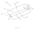
- Fig. 1 depicts a representative PMOSFET device 10 , which may be a discrete device or part of an integrated circuit. Cross sections through the device 10 are shown schematically in Figs. 2 and 3. In this particular embodiment of the PMOSFET device 10, the device 10 has been constructed on the surface of a piece of single crystal silicon 12 surrounded by an isolation oxide 20. This type of design and construction is often termed shallow trench isolation (STI), or local oxidation of silicon (LOCOS).
- STI shallow trench isolation
- LOCS local oxidation of silicon
- the surface of the single crystal silicon 12 is doped with an element such as phosphorus, arsenic, or antimony to create a zone of n-type silicon 14 (see Figs 2 and 3).
- An electrically nonconductive substance typically silicon dioxide, which represents a preferred embodiment of the present invention, is used as the isolation oxide 20 to provide electrical isolation from other active devices fabricated on the same silicon substrate.
- a thin insulation layer 30, typically silicon dioxide or silicon nitride, is applied to the top of the single crystal silicon 12; portions of this oxide insulation layer 30 are subsequently stripped away to expose source and drain regions of the device, 40 and 50, respectively. The remaining portion of the insulating layer 30 may be termed the gate oxide layer.
- a layer of polycrystalline silicon is applied above the gate oxide layer forms the gate 60.
- Electrical connections between other components of an integrated device and the source 40, drain 50, and gate 60 are shown schematically at 42, 52, and 62, respectively. In practice, these connections may be layers of metallic materials deposited onto selected portions of an integrated circuit to interconnect the various elements of the circuit, as required by the design of the circuit.
- the source 40 and drain 50 are doped, typically by the diffusion of boron, to become p-type semiconductors.
- a region of the single crystal silicon lying between the source 40 and drain 50 and beneath the gate insulation layer 30 is carefully maintained as n-type material and forms the channel 45. Electric current can flow through a PMOSFET between the source and drain when a sufficiently small negative voltage is applied to the gate. This is the basic function of the FET.
- the particular problem addressed by the present invention exists at the sidewall comer interfaces 64 and 66 shown in Fig. 1.
- the sidewall corner interface 64 is shown in cross section in Fig. 3.
- the sidewall corner interfaces 64 and 66 are located at both ends of the gate 60 and are distinguishable from the main section 68 of the gate 60 between the two sidewalls.
- Each sidewall has a generally vertical orientation, and the combination of that orientation, plus structural characteristics of the materials in the sidewall corner areas, lead to electrical functionality that differs from performance in central portions of the device 10 .
- a PMOSFET device has a characteristic threshold voltage; when such a voltage is applied to the gate, the device is shifted into an activated or "on" state.
- a less negative threshold voltage implies that the device is readily turned on. If operating conditions of a device admit to its being activated inadvertently, the device cannot function according to its design intent. In particular, for a PMOSFET device that can be activated (i.e., allowing holes to flow from source to drain) despite a normally high voltage applied to its gate, a significant parasitic current or "off current” can flow through the device.
- the "off current” represents a characteristic of the device itself, rather than the operating parameters imposed on the device.
- the solution to the PMOSFET sidewall corner interface hot carrier-induced instability is attained using a localized nitrogen implantation into the interface area between the isolation oxide 20 and the single crystal silicon 12 along the active channel 45 of the device 10, which results in an elevated nitrogen content within the portion 70 of the channel 45 nearest the sidewall (see Fig. 3).
- This implant must be done at least locally along the interface.
- a block mask is required to protect the channel area from the nitrogen implant while implanting in the channel region along the interface. The block mask assures that the threshold voltage of the main device is not perturbed by the nitrogen implant.
- the same nitrogen implantation used to grow the oxide can be used to implant the sidewall corner interface reducing the parasitic sidewall corner PMOSFET instability. If the dose and energy selected for the uniform nitrogen implant to grow the gate oxide are not adequate to reduce the sensitivity to the parasitic PMOSFET sidewall corner activation, then an extra localized nitrogen implant along the sidewall corner and silicon interface is needed. This procedure represents a second sub-step in the process.
- the term “device” includes both discrete devices consisting of a single transistor, or integrated circuit devices comprising many transistors.
- the present invention is particularly applicable to integrated circuit devices, and the manufacture of such devices, and that application constitutes a preferred embodiment of the invention.
- the nitrogen implanted in the PMOSFET device 10 is preferably supplied to the implantation apparatus in the molecular form (N 2 ).
- DRAM dynamic random access memory
- the advantages of cost per bit, device density, and flexibility of use i.e., both read and write operations are possible have made DRAM cells the most widely used form of semiconductor memory to date.
- the earliest DRAM cells were three-transistor cells. Today, DRAM cells consisting of only one transistor and one capacitor have been implemented.
- a control group of four devices was made using customary production line technology. Two groups, containing five and nine devices, were subjected to nitrogen molecule implantation doses of 1.0 x 10 14 and 1.5 x 10 14 ions per square centimeter, respectively. All implantation was done at an energy level of 12 keV. The sidewall threshold voltage was measured for each device. These data are presented in Fig. 4. Note that there was a clear decrease in sidewall threshold voltage, V th (Sidewall), as the dosage of nitrogen ion implantation was increased.
Landscapes
- Insulated Gate Type Field-Effect Transistor (AREA)
- Metal-Oxide And Bipolar Metal-Oxide Semiconductor Integrated Circuits (AREA)
Applications Claiming Priority (2)
| Application Number | Priority Date | Filing Date | Title |
|---|---|---|---|
| US09/511,395 US6724053B1 (en) | 2000-02-23 | 2000-02-23 | PMOSFET device with localized nitrogen sidewall implantation |
| US511395 | 2000-02-23 |
Publications (3)
| Publication Number | Publication Date |
|---|---|
| EP1128427A2 true EP1128427A2 (fr) | 2001-08-29 |
| EP1128427A8 EP1128427A8 (fr) | 2001-11-28 |
| EP1128427A3 EP1128427A3 (fr) | 2004-10-13 |
Family
ID=24034717
Family Applications (1)
| Application Number | Title | Priority Date | Filing Date |
|---|---|---|---|
| EP20010301600 Withdrawn EP1128427A3 (fr) | 2000-02-23 | 2001-02-22 | Fabrication de dispositifs semi-conducteurs |
Country Status (3)
| Country | Link |
|---|---|
| US (1) | US6724053B1 (fr) |
| EP (1) | EP1128427A3 (fr) |
| TW (1) | TW503577B (fr) |
Cited By (1)
| Publication number | Priority date | Publication date | Assignee | Title |
|---|---|---|---|---|
| US7989882B2 (en) | 2007-12-07 | 2011-08-02 | Cree, Inc. | Transistor with A-face conductive channel and trench protecting well region |
Families Citing this family (6)
| Publication number | Priority date | Publication date | Assignee | Title |
|---|---|---|---|---|
| US20060079046A1 (en) * | 2004-10-12 | 2006-04-13 | International Business Machines Corporation | Method and structure for improving cmos device reliability using combinations of insulating materials |
| US7288451B2 (en) * | 2005-03-01 | 2007-10-30 | International Business Machines Corporation | Method and structure for forming self-aligned, dual stress liner for CMOS devices |
| US7101744B1 (en) | 2005-03-01 | 2006-09-05 | International Business Machines Corporation | Method for forming self-aligned, dual silicon nitride liner for CMOS devices |
| US8247877B2 (en) * | 2009-08-31 | 2012-08-21 | International Business Machines Corporation | Structure with reduced fringe capacitance |
| US8222093B2 (en) * | 2010-02-17 | 2012-07-17 | GlobalFoundries, Inc. | Methods for forming barrier regions within regions of insulating material resulting in outgassing paths from the insulating material and related devices |
| TWM514577U (zh) | 2015-07-23 | 2015-12-21 | 胡聯雄 | 折射透鏡以及具有該折射透鏡之片狀結構 |
Family Cites Families (24)
| Publication number | Priority date | Publication date | Assignee | Title |
|---|---|---|---|---|
| JPS56118348A (en) * | 1980-02-22 | 1981-09-17 | Fujitsu Ltd | Semiconductor device |
| NL187328C (nl) | 1980-12-23 | 1991-08-16 | Philips Nv | Werkwijze ter vervaardiging van een halfgeleiderinrichting. |
| US4774197A (en) | 1986-06-17 | 1988-09-27 | Advanced Micro Devices, Inc. | Method of improving silicon dioxide |
| US5330920A (en) | 1993-06-15 | 1994-07-19 | Digital Equipment Corporation | Method of controlling gate oxide thickness in the fabrication of semiconductor devices |
| US5514902A (en) * | 1993-09-16 | 1996-05-07 | Mitsubishi Denki Kabushiki Kaisha | Semiconductor device having MOS transistor |
| US5468657A (en) | 1994-06-17 | 1995-11-21 | Sharp Microelectronics Technology, Inc. | Nitridation of SIMOX buried oxide |
| JP3015253B2 (ja) * | 1994-06-22 | 2000-03-06 | 三菱電機株式会社 | 半導体装置およびその製造方法 |
| US5643822A (en) * | 1995-01-10 | 1997-07-01 | International Business Machines Corporation | Method for forming trench-isolated FET devices |
| US5674788A (en) | 1995-06-06 | 1997-10-07 | Advanced Micro Devices, Inc. | Method of forming high pressure silicon oxynitride gate dielectrics |
| US5589407A (en) | 1995-09-06 | 1996-12-31 | Implanted Material Technology, Inc. | Method of treating silicon to obtain thin, buried insulating layer |
| TW328147B (en) | 1996-05-07 | 1998-03-11 | Lucent Technologies Inc | Semiconductor device fabrication |
| JP4014677B2 (ja) * | 1996-08-13 | 2007-11-28 | 株式会社半導体エネルギー研究所 | 絶縁ゲイト型半導体装置 |
| US5909622A (en) | 1996-10-01 | 1999-06-01 | Advanced Micro Devices, Inc. | Asymmetrical p-channel transistor formed by nitrided oxide and large tilt angle LDD implant |
| US5893739A (en) | 1996-10-01 | 1999-04-13 | Advanced Micro Devices, Inc. | Asymmetrical P-channel transistor having a boron migration barrier and a selectively formed sidewall spacer |
| JP3684520B2 (ja) * | 1997-02-03 | 2005-08-17 | 富士通株式会社 | 半導体装置及びその製造方法 |
| US5861335A (en) | 1997-03-21 | 1999-01-19 | Advanced Micro Devices, Inc. | Semiconductor fabrication employing a post-implant anneal within a low temperature high pressure nitrogen ambient to improve channel and gate oxide reliability |
| US6225151B1 (en) * | 1997-06-09 | 2001-05-01 | Advanced Micro Devices, Inc. | Nitrogen liner beneath transistor source/drain regions to retard dopant diffusion |
| US5851893A (en) | 1997-07-18 | 1998-12-22 | Advanced Micro Devices, Inc. | Method of making transistor having a gate dielectric which is substantially resistant to drain-side hot carrier injection |
| JP3125719B2 (ja) * | 1997-07-28 | 2001-01-22 | 日本電気株式会社 | 半導体装置及びその製造方法 |
| JPH1187697A (ja) * | 1997-09-01 | 1999-03-30 | Toshiba Corp | 半導体製造方法、半導体記憶装置の製造方法、および半導体装置 |
| JP3064994B2 (ja) * | 1997-10-31 | 2000-07-12 | 日本電気株式会社 | 半導体装置及びその製造方法 |
| US6025238A (en) * | 1997-12-18 | 2000-02-15 | Advanced Micro Devices | Semiconductor device having an nitrogen-rich punchthrough region and fabrication thereof |
| US6030875A (en) * | 1997-12-19 | 2000-02-29 | Advanced Micro Devices, Inc. | Method for making semiconductor device having nitrogen-rich active region-channel interface |
| US6221724B1 (en) * | 1998-11-06 | 2001-04-24 | Advanced Micro Devices, Inc. | Method of fabricating an integrated circuit having punch-through suppression |
-
2000
- 2000-02-23 US US09/511,395 patent/US6724053B1/en not_active Expired - Lifetime
-
2001
- 2001-02-22 TW TW090104049A patent/TW503577B/zh not_active IP Right Cessation
- 2001-02-22 EP EP20010301600 patent/EP1128427A3/fr not_active Withdrawn
Cited By (3)
| Publication number | Priority date | Publication date | Assignee | Title |
|---|---|---|---|---|
| US7989882B2 (en) | 2007-12-07 | 2011-08-02 | Cree, Inc. | Transistor with A-face conductive channel and trench protecting well region |
| US8211770B2 (en) | 2007-12-07 | 2012-07-03 | Cree, Inc. | Transistor with A-face conductive channel and trench protecting well region |
| US9064710B2 (en) | 2007-12-07 | 2015-06-23 | Cree, Inc. | Transistor with A-face conductive channel and trench protecting well region |
Also Published As
| Publication number | Publication date |
|---|---|
| TW503577B (en) | 2002-09-21 |
| US6724053B1 (en) | 2004-04-20 |
| EP1128427A3 (fr) | 2004-10-13 |
| EP1128427A8 (fr) | 2001-11-28 |
Similar Documents
| Publication | Publication Date | Title |
|---|---|---|
| US4701776A (en) | MOS floating gate memory cell and process for fabricating same | |
| US4822750A (en) | MOS floating gate memory cell containing tunneling diffusion region in contact with drain and extending under edges of field oxide | |
| US6479866B1 (en) | SOI device with self-aligned selective damage implant, and method | |
| US5712173A (en) | Method of making semiconductor device with self-aligned insulator | |
| US7064399B2 (en) | Advanced CMOS using super steep retrograde wells | |
| US4116720A (en) | Method of making a V-MOS field effect transistor for a dynamic memory cell having improved capacitance | |
| KR100735654B1 (ko) | 디커플링 캐패시터 및 그 제조 방법 | |
| KR100913830B1 (ko) | 완전 공핍 실리콘 온 인슐레이터 구조에 대한 도핑 방법및 그 방법으로 도핑된 영역을 포함하는 장치 | |
| US5292676A (en) | Self-aligned low resistance buried contact process | |
| US7180136B2 (en) | Biased, triple-well fully depleted SOI structure | |
| US6444548B2 (en) | Bitline diffusion with halo for improved array threshold voltage control | |
| US6300207B1 (en) | Depleted sidewall-poly LDD transistor | |
| Chan et al. | Recessed-channel structure for fabricating ultrathin SOI MOSFET with low series resistance | |
| US4878100A (en) | Triple-implanted drain in transistor made by oxide sidewall-spacer method | |
| US6495887B1 (en) | Argon implantation after silicidation for improved floating-body effects | |
| KR100276744B1 (ko) | Ldd구조를 갖는 반도체 장치와 그 제조방법 | |
| US6724053B1 (en) | PMOSFET device with localized nitrogen sidewall implantation | |
| US5242849A (en) | Method for the fabrication of MOS devices | |
| US5672524A (en) | Three-dimensional complementary field effect transistor process | |
| KR0140715B1 (ko) | 반도체 집적회로 구조물 및 그 제조방법 | |
| JPH0799259A (ja) | 縦型バイポーラトランジスタを有するBi−CMOS SOI構造及びその製造方法 | |
| US4225879A (en) | V-MOS Field effect transistor for a dynamic memory cell having improved capacitance | |
| US5939757A (en) | Semiconductor device having triple well structure | |
| KR950008257B1 (ko) | 모스(mos) 트랜지스터 및 그 제조방법 | |
| US20030207531A1 (en) | Method for forming polysilicon connected deep trench dram cell |
Legal Events
| Date | Code | Title | Description |
|---|---|---|---|
| PUAI | Public reference made under article 153(3) epc to a published international application that has entered the european phase |
Free format text: ORIGINAL CODE: 0009012 |
|
| AK | Designated contracting states |
Kind code of ref document: A2 Designated state(s): AT BE CH CY DE DK ES FI FR GB GR IE IT LI LU MC NL PT SE TR |
|
| AX | Request for extension of the european patent |
Free format text: AL;LT;LV;MK;RO;SI |
|
| RIN1 | Information on inventor provided before grant (corrected) |
Inventor name: RENGARAJAN, RAJESH Inventor name: KATSUMATA, RYOTA, C/O KABUSHIKI KAISHA TOSHIBA Inventor name: WEYBRIGHT, MARY E. Inventor name: LA ROSA, GIUSEPPE Inventor name: DIVAKARUNI, RUNI |
|
| PUAL | Search report despatched |
Free format text: ORIGINAL CODE: 0009013 |
|
| AK | Designated contracting states |
Kind code of ref document: A3 Designated state(s): AT BE CH CY DE DK ES FI FR GB GR IE IT LI LU MC NL PT SE TR |
|
| AX | Request for extension of the european patent |
Extension state: AL LT LV MK RO SI |
|
| RAP1 | Party data changed (applicant data changed or rights of an application transferred) |
Owner name: KABUSHIKI KAISHA TOSHIBA Owner name: INTERNATIONAL BUSINESS MACHINES CORPORATION Owner name: INFINEON TECHNOLOGIES AG |
|
| RAP1 | Party data changed (applicant data changed or rights of an application transferred) |
Owner name: KABUSHIKI KAISHA TOSHIBA Owner name: INTERNATIONAL BUSINESS MACHINES CORPORATION Owner name: INFINEON TECHNOLOGIES NORTH AMERICA CORP. |
|
| RAP1 | Party data changed (applicant data changed or rights of an application transferred) |
Owner name: KABUSHIKI KAISHA TOSHIBA Owner name: INTERNATIONAL BUSINESS MACHINES CORPORATION Owner name: INFINEON TECHNOLOGIES AG |
|
| 17P | Request for examination filed |
Effective date: 20050211 |
|
| AKX | Designation fees paid |
Designated state(s): DE FR GB IT |
|
| 17Q | First examination report despatched |
Effective date: 20050627 |
|
| GRAP | Despatch of communication of intention to grant a patent |
Free format text: ORIGINAL CODE: EPIDOSNIGR1 |
|
| STAA | Information on the status of an ep patent application or granted ep patent |
Free format text: STATUS: THE APPLICATION IS DEEMED TO BE WITHDRAWN |
|
| 18D | Application deemed to be withdrawn |
Effective date: 20070703 |