EP1128445A2 - Interconnexion pour cellules photovoltaiques dans le même plan avec languette pour une diode intégrée - Google Patents
Interconnexion pour cellules photovoltaiques dans le même plan avec languette pour une diode intégrée Download PDFInfo
- Publication number
- EP1128445A2 EP1128445A2 EP01104278A EP01104278A EP1128445A2 EP 1128445 A2 EP1128445 A2 EP 1128445A2 EP 01104278 A EP01104278 A EP 01104278A EP 01104278 A EP01104278 A EP 01104278A EP 1128445 A2 EP1128445 A2 EP 1128445A2
- Authority
- EP
- European Patent Office
- Prior art keywords
- solar cell
- interconnect
- diode
- tab
- base portion
- Prior art date
- Legal status (The legal status is an assumption and is not a legal conclusion. Google has not performed a legal analysis and makes no representation as to the accuracy of the status listed.)
- Granted
Links
- 239000000463 material Substances 0.000 claims description 12
- 230000000737 periodic effect Effects 0.000 claims description 4
- 230000000712 assembly Effects 0.000 description 16
- 238000000429 assembly Methods 0.000 description 16
- BQCADISMDOOEFD-UHFFFAOYSA-N Silver Chemical compound [Ag] BQCADISMDOOEFD-UHFFFAOYSA-N 0.000 description 12
- 229910052709 silver Inorganic materials 0.000 description 12
- 239000004332 silver Substances 0.000 description 12
- 238000013461 design Methods 0.000 description 11
- 239000006059 cover glass Substances 0.000 description 10
- 239000010432 diamond Substances 0.000 description 8
- 229910000833 kovar Inorganic materials 0.000 description 7
- 239000000853 adhesive Substances 0.000 description 6
- 230000001070 adhesive effect Effects 0.000 description 6
- 229910003460 diamond Inorganic materials 0.000 description 5
- 239000010410 layer Substances 0.000 description 5
- 239000000758 substrate Substances 0.000 description 5
- 238000003466 welding Methods 0.000 description 5
- ZOKXTWBITQBERF-UHFFFAOYSA-N Molybdenum Chemical compound [Mo] ZOKXTWBITQBERF-UHFFFAOYSA-N 0.000 description 4
- 238000000034 method Methods 0.000 description 4
- 229910052750 molybdenum Inorganic materials 0.000 description 4
- 239000011733 molybdenum Substances 0.000 description 4
- 238000005382 thermal cycling Methods 0.000 description 4
- 239000012790 adhesive layer Substances 0.000 description 3
- 238000006243 chemical reaction Methods 0.000 description 3
- 239000011248 coating agent Substances 0.000 description 3
- 238000000576 coating method Methods 0.000 description 3
- 238000009413 insulation Methods 0.000 description 3
- 238000004519 manufacturing process Methods 0.000 description 3
- 238000012545 processing Methods 0.000 description 3
- 230000002441 reversible effect Effects 0.000 description 3
- 238000012360 testing method Methods 0.000 description 3
- 229910001374 Invar Inorganic materials 0.000 description 2
- 230000008901 benefit Effects 0.000 description 2
- 230000015556 catabolic process Effects 0.000 description 2
- 230000005779 cell damage Effects 0.000 description 2
- 208000037887 cell injury Diseases 0.000 description 2
- 238000004140 cleaning Methods 0.000 description 2
- 238000011109 contamination Methods 0.000 description 2
- 230000006378 damage Effects 0.000 description 2
- 238000007747 plating Methods 0.000 description 2
- 230000005855 radiation Effects 0.000 description 2
- 238000005476 soldering Methods 0.000 description 2
- JBRZTFJDHDCESZ-UHFFFAOYSA-N AsGa Chemical compound [As]#[Ga] JBRZTFJDHDCESZ-UHFFFAOYSA-N 0.000 description 1
- OKTJSMMVPCPJKN-UHFFFAOYSA-N Carbon Chemical compound [C] OKTJSMMVPCPJKN-UHFFFAOYSA-N 0.000 description 1
- 229910001218 Gallium arsenide Inorganic materials 0.000 description 1
- VYPSYNLAJGMNEJ-UHFFFAOYSA-N Silicium dioxide Chemical compound O=[Si]=O VYPSYNLAJGMNEJ-UHFFFAOYSA-N 0.000 description 1
- 239000003522 acrylic cement Substances 0.000 description 1
- 238000005253 cladding Methods 0.000 description 1
- 238000010276 construction Methods 0.000 description 1
- 230000008602 contraction Effects 0.000 description 1
- 238000009826 distribution Methods 0.000 description 1
- 230000000694 effects Effects 0.000 description 1
- 230000005611 electricity Effects 0.000 description 1
- 239000005350 fused silica glass Substances 0.000 description 1
- 229910052732 germanium Inorganic materials 0.000 description 1
- GNPVGFCGXDBREM-UHFFFAOYSA-N germanium atom Chemical compound [Ge] GNPVGFCGXDBREM-UHFFFAOYSA-N 0.000 description 1
- 229910002804 graphite Inorganic materials 0.000 description 1
- 239000010439 graphite Substances 0.000 description 1
- 230000000873 masking effect Effects 0.000 description 1
- 238000012986 modification Methods 0.000 description 1
- 230000004048 modification Effects 0.000 description 1
- 239000003921 oil Substances 0.000 description 1
- 229920003223 poly(pyromellitimide-1,4-diphenyl ether) Polymers 0.000 description 1
- 229920001296 polysiloxane Polymers 0.000 description 1
- 239000004065 semiconductor Substances 0.000 description 1
- 229910052710 silicon Inorganic materials 0.000 description 1
- 239000010703 silicon Substances 0.000 description 1
Images



Classifications
-
- H—ELECTRICITY
- H10—SEMICONDUCTOR DEVICES; ELECTRIC SOLID-STATE DEVICES NOT OTHERWISE PROVIDED FOR
- H10F—INORGANIC SEMICONDUCTOR DEVICES SENSITIVE TO INFRARED RADIATION, LIGHT, ELECTROMAGNETIC RADIATION OF SHORTER WAVELENGTH OR CORPUSCULAR RADIATION
- H10F19/00—Integrated devices, or assemblies of multiple devices, comprising at least one photovoltaic cell covered by group H10F10/00, e.g. photovoltaic modules
- H10F19/90—Structures for connecting between photovoltaic cells, e.g. interconnections or insulating spacers
- H10F19/902—Structures for connecting between photovoltaic cells, e.g. interconnections or insulating spacers for series or parallel connection of photovoltaic cells
- H10F19/904—Structures for connecting between photovoltaic cells, e.g. interconnections or insulating spacers for series or parallel connection of photovoltaic cells characterised by the shapes of the structures
-
- H—ELECTRICITY
- H10—SEMICONDUCTOR DEVICES; ELECTRIC SOLID-STATE DEVICES NOT OTHERWISE PROVIDED FOR
- H10F—INORGANIC SEMICONDUCTOR DEVICES SENSITIVE TO INFRARED RADIATION, LIGHT, ELECTROMAGNETIC RADIATION OF SHORTER WAVELENGTH OR CORPUSCULAR RADIATION
- H10F19/00—Integrated devices, or assemblies of multiple devices, comprising at least one photovoltaic cell covered by group H10F10/00, e.g. photovoltaic modules
- H10F19/70—Integrated devices, or assemblies of multiple devices, comprising at least one photovoltaic cell covered by group H10F10/00, e.g. photovoltaic modules comprising bypass diodes
- H10F19/75—Integrated devices, or assemblies of multiple devices, comprising at least one photovoltaic cell covered by group H10F10/00, e.g. photovoltaic modules comprising bypass diodes the bypass diodes being integrated or directly associated with the photovoltaic cells, e.g. formed in or on the same substrate
-
- Y—GENERAL TAGGING OF NEW TECHNOLOGICAL DEVELOPMENTS; GENERAL TAGGING OF CROSS-SECTIONAL TECHNOLOGIES SPANNING OVER SEVERAL SECTIONS OF THE IPC; TECHNICAL SUBJECTS COVERED BY FORMER USPC CROSS-REFERENCE ART COLLECTIONS [XRACs] AND DIGESTS
- Y02—TECHNOLOGIES OR APPLICATIONS FOR MITIGATION OR ADAPTATION AGAINST CLIMATE CHANGE
- Y02E—REDUCTION OF GREENHOUSE GAS [GHG] EMISSIONS, RELATED TO ENERGY GENERATION, TRANSMISSION OR DISTRIBUTION
- Y02E10/00—Energy generation through renewable energy sources
- Y02E10/50—Photovoltaic [PV] energy
Definitions
- the present invention generally relates to solar cells and solar cell panels and in particular to solar cell interconnects. More specifically, the invention relates to an improved in-plane solar cell interconnect that supports a diode on one side of the solar cell.
- Attachment of the diode to each cell is in addition to attaching interconnects for the purpose of Increasing volinge in a solar cell circuit by series connection.
- a number of the stacked arrangements or cells is provided in the form of an array on a substrate or multiple substrates.
- Interconnects are used in an array of solar cells to electrically connect the cells to one another in series, in parallel or both. They must be designed robust to survive the rigors of the space environment.
- the individual solar cells and their substrale can be subject to significant mechanical vibration during a launch and thermal cycling during the course of the spacecraft's mission in space.
- the thermal cycling in tum, leads to thermal expansion and contraction of the various materials. This can cause stress on the interconnects if there is a coefficient of expansion (CTE) mismatch between the cells and the substrate materials.
- CTE coefficient of expansion
- a solar panel in which the interconnect is utilized will have a shorter life expectancy.
- the spacecraft on which the solar panel is used will have a shorter life and result In greater costs to replace it.
- a conductive interconnect that is separate from the interconnect tab connects the anode contact of the diode to the p-contact of the next assombly.
- a drawback to this design is the difficully in removing and replacing an individual solar cell from an array without damaging adjoining cells and structures.
- FIG. 1 depicts another interconnect design that has been used with solar cell assemblies containing a diode on the back side.
- a first solar cell assembly 10 includes a cover glass 12 disposed over an ohmic bar with adhesive 13. The ohmic bar is on the top surface of a solar cell 14.
- a wraparound diode tab 17 is fixed to a front side of the assembly 10 and wraps around to the back side of the assembly 10 to hold a diode 16 in place on the back side. Between the diode tab 17 and the solar cell 14 is an insulation 18.
- An adhesive layer 15 adheres the diode 16 to the solar cell 14.
- an interconnect 19 electrically connects the first solar cell assembly 10 to a second solar cell assembly 11. Typically, three interconnects 19 are used between the adjacent solar cell assemblies 10 and 11, such as when each assembly is about 7cm x 3.5cm.
- each weld pulse can degrade the electrical performance of the solar cell assembly 10 due to shunting.
- a small shunt reduces the electrical output of the solar cell 14 by leaking current across the junction or junctions of the cell 14, thus reducing its conversion efficiency.
- a severe shunt results in rejecting the expensive cell 14 completely.
- the diode tab 17 places a strain on the ohmic weld joint and cover glass 12. Because of the thermal and mechanical stresses impartod on the bonded solar cell 14 in long life missions, the interconnect 19 is typically made with a strong material such as Kovar, Invar, and molybdenum, On the other hand, the strong materials make the interconnect 19 stiffer.
- the tab 17 When the diode tab 17 is bent around in a wraparound configuration, the tab 17 has a tendency to both delaminate or even shatter a thin cover glass 12, as well as to do-weld from the ohmic bar on the front surface of the solar cell 14. This condition can render the diode 16 useless for protecting the cell 14 from reverse current and also can reduce the ability of the cover glass 12 to protect the cell 14 from radiation damage. These two conditions can then reduce the power of an entire solar cell circuit connected in series with the damaged cell 14.
- interconnects that achieve the following functions or have the following characteristics: electrical connection between adjacent solar cells, as well as back to front connection for a diode mounted on the backside of a single cell; improved resistance to thermal cycling; flexure in an in-plane configuration; connection to tho cell with a minimum number of processing steps and cell interconnection that minimizes the number of welds so that the potential for cell damage is minimized.
- An in-plane solar cell interconnect is also needed to reduce the potential amount of shading to active areas of the cell and to facilitate cleaning of bonding adhesive off the top surface of a cover glass.
- the present invention is directed to an improved interconnect for connecting first and second solar cells.
- the interconnect comprises a base portion having a first distal section and a first intermediate section, with the first distal and intermediate sections being integral with the base portion and capable of fixture to the first solar cell.
- An extension tab is integral to the first distal section, with the extension tab being capable of fixture to a front side of the second solar cell.
- a diode tab is integral to the first intermediate section, with the diode tab being capable of fixture to a diodo side of the second solar cell, such diode side being on a side opposite to the front side.
- the present invention is applicable both to solar cells used for terrestrial applications as well as non-terrestrial applications such as on satellites and airplanes and high altitude platforms and vehicles.
- FIG. 2 is a side cross-sectional viow of a two solar cell assemblies 20, 37 having an interconnect 26 affixed therebetween according to one embodiment of the present invention.
- the solar cell assemblies 20, 37 do not form a part of the present invention but are illustrated for purposes of understanding the design and operation of the interconnect 26. Accordingly, the solar cell assemblies 20, 37 can be constructed according to any well-known design in the art, such as the following. Additionally, while the present invention can be used in various contexts, the present invention is particularly useful in the context of a satellite 40 (FIG. 11) having a solar panel 41 comprising a plurality of solar cell assemblies 20, 37.
- the solar cell assembly 20 includes a cover glass 21 that serves to protect the assembly 20 from radiation damage.
- the cover glass 21 is typically made of materials such as fused silica or microsheet.
- the adhesive layer 22 can be made of various materials, such as polymeric silicone, and is oftentimes about 3 mils thick.
- the solar cell 23 is constructed of semiconductor layers according to well known methods in the art. Although it can vary, the solar cell 23 is typically on the order of about 7 mils thick.
- a bypass diode 24 is usually about 3 mils thick and affixed to a back (or non-illuminated) side of the solar cell 23 which is opposite of the front side. Also affixed to the back side of the solar cell 23 is an insulation layer 25 that insulates the solar cell 23 from a diode tab 29 of the interconnect 26.
- the insulation layer 25 may be made, for example, from kapton with acrylic adhesive, and is oftentimes about 1 mil thick,
- the interconnect 26, in this embodiment, includes an integral base or stress relief portion 28, a plurality of integral extension tabs 27, and an integral diode tab 29.
- the diode lab 29 supports the diode 24 in position at the back side of the solar cell 23, as well as providing electrical connection from the back side and to the front side of the assembly 20.
- the extension tabs 27 connect an ohmic bar (not shown) located on the front side of the solar cell 23 to a second solar cell assembly 37.
- the second solar cell assembly 37 can be identical in construction as the first solar cell assembly 20, but is only partially shown in FIG. 2. While subject to variation, the distance between the first and second solar cell assemblies is about 10 to 30 mils.
- the height between the extension tabs 27 and the diode tab 29 is about 8 mils.
- the base portion 28, extension tabs 27 and diode tab 29 are each about 1-2 mils thick, which can include a silver coating, as described below, on opposing surfaces of the interconnect 26.
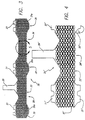
- the base or stress relief portion 28 comprises an integrally formed first distal section 30, a second distal section 31, and a mid section 32 therebetween (FIG. 3).
- the stress relief portion 28 further includes a first intermediate section 33 that is disposed between the first distal section 30 and the mid section 32.
- a second Intermediate section 34 of the stress relief portion 28 is disposed between the mid section 32 and the second distal section 31.
- the mid sections 33, 34 have a rectangular configuration.
- the first and second distal sections 30, 31, as well as the mid section 32 have an octagon configuration. With such octagon configurations, the first distal section 30 includes a connecting portion 30a, the second distal section 31 includes a connecting portion 31a, and the mid section 32 includes a connecting portion 32a. All of the connecting portions 30a, 31a, 32a are on a side of their respective sections opposite the extension tabs 27. Notwithstanding the foregoing, the present invention contemplates that other configurations can be utilized.
- the plurality of extension tabs 27 and the diode tab 29 are integrally formed with the base portion 28 along a first edge or side that can be immediately adjacent the first solar cell assembly 20.
- the second or opposite edge of the base portion 28 can then be immediately adjacent the second solar cell assembly 37.
- the connecting portions 30a, 31a, 32a can be affixed to the second solar cell assembly 37, such as at its back side (FIG. 2) by soldering.
- the extension tabs 27 aro affixed (such as by welding) onto the front side of the first solar cell assembly 20 and the diode tab 29 can be affixed onto the diode or back side of the first solar cell assembly 20 (FIG. 1).
- FIG. 3 While the preferred embodiment shown (FIG. 3) includes two extension tabs 27 integrally formed on the first and second distal sections 30, 31, as well as the mid section 32, more or less than two tab 27 can be used. Further, the number of tabs 27 need not be the same for each section 30, 31, 32.
- an interconnect 26' includes a base portion 28' that comprises a first distal section 30', an intermediate section 33' and a mid section 32'.
- On a first side of the base portion 28' are a plurality of first extension tabs 27'.
- this embodiment includes a plurality second extension tabs 35' positioned on a second side of the base portion 28' that is opposite the first extension tabs 27'.
- the second extension tabs 35' take the place of the connecting portions 30a, 31a, 32a of the above embodiment.
- Fig. 4 illustrates the preferred embodiment for welding of cell assembly 20 to cell assembly 37.
- the preferred method of fixture is by welding because of it being a less costly and more reliable process than soldering.
- the interconnect 26 (26') provides a substantially in-plane profile to the first and second solar cell assemblies 20, 37.
- the interconnect 26 (26') when viewed from the side, extends minimally above and below the heights of the solar cell assemblies 20, 37.
- the interconnect 26 (26') minimizes the amount of shading that can occur to the active or front sides of the assemblies 20, 37.
- An in-plane profile also minimizes the amount of adhesive that can be transferred to the front sides of the assemblies 20, 37,
- the assemblies 20, 37 are typically adhered at their back sides to a substrate. The adhesive used for bonding tends to flow up between adjoining cell assemblies, over an interconnect, and across the front sides of the assemblies, particularly when the interconnect is higher than the heights of the assemblies.
- the interconnect 26 is made of strong material such as Invar, Kovar or molybdenum.
- a silver coating is used over the abovementioned matorial, which enables easier welding of the interconnect 26 to the silver that is typically used on the front and back sides of the solar cell 23.
- the silver coating on the interconnect 26 may be a plated or clad material. The latter is preferred because it has a lighter thickness tolerance and there is less chanco of contamination. Plated material is not as easily controlled as cladding and the silver thickness can vary over 200 micro-inches per side. Plating also can result in contamination from uncleaned plating solutions or oils.
- the area of the base or stress relief portion 28 can be seen as constructed with a material having a periodic pattern.
- the periodic pattern is in the shape of an oval.
- FIG 5 depicts another oval pattern, but which has more connections between adjoining ovals when compared to that in FIG.4.
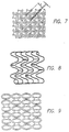
- the pattern is in the form of diamonds
- FIG. 7 is in the form of S's
- FIG. 8 is in tho form of sine waves
- FIG. 9 is in the form of yet another embodiment of ovals.
- the particular size of the shapes constituting the pattern in the base portion 28 can vary.
- the distance "a" from one center of an oval to the next center in a lengthwise direction can vary between about .040" to .080".
- the lengthwise distance "b" of a single oval can vary between about .030" to .100.
- the distance "c” from one center of an oval to the next center based on height can vary between about .020" to .050".
- the distance "d” of the thickness of an oval can vary between about .003"to .010".
- an angle “o” varies between about 30° to 60°, as does angle "f.”
- the end-to-end distance “g” between two adjacent diamonds is between about ..006" to .020".
- the length of a diamond “h” varies from about .020" to .060".
- the height of a diamond “i” is about .010” to .040".
- the height-to-height distance “j” between two diamonds is about .006" to .020.
- a distance "k” between two S's varies from about .020" to .100".
- a thickness "I” of an S varies from about .003" to .010".
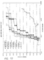
- FIG. 10 depicts the test results of seven embodiments of the interconnect 26 that was subjected to cycled flexures of 5 mils in a lateral direction.
- the embodiment (A) was made of silver plated Kovar in the diamond configuration of FIG. 6.
- the embodiment (B) was made of silver plated Kovar in the oval configuration of FIG. 5.
- the embodiment (C) was made of silver clad Kovar in the diamond configuration of FIG. 6.
- Silver clad Kovar in an oval configuration of FIG. 5 was used for embodiment (D).
- Silver clad molybdenum in a diamond configuration of FIG. 6 was used for embodiment (E).
- Embodiment (F) was silver clad molybdenum in an oval configuration of FIG. 5.
- Embodiment (G) was silver clad kovar in an oval configuration of FIG. 9.
- embodiment (G) provided the best results in terms of failure rate at high cycles.
- all embodiments provided acceptable results when it is considered that in a 15 year GEO space mission, the interconnects undergo only about 1800 thermal cycles and in an LEO space mission the interconnects undergo only about 20,000 to 40,000 cycles in a typical spacecraft lifetime.
- the interconnects undergo flexure of about 2-3 mils on a graphite substrate, even though the test condition was 5 mils to expedite the test.
- the present invention provides an apparatus that connects solar cells in series, as well as connect a diode from the back of a cell to the front.
- the present invention also provides improved resistance to thermal cycling and increased flexure.
- the interconnect of the present invention can be manufactured with a minimum number of processing steps, as well as a minimum number of welds so that the potential for cell damage is minimized.
- the in-plane nature of the present invention also reduces the potential amount of shading to active areas of the cell.
- the in-plane feature reduces breakage associated with cleaning cured adhesive from the top surface of fragile, germanium or gallium arsenide based thin solar cells. This results from the fact that cell masking can lay flat in the inter-cell spaces, thus reducing adhesive squeeze-out onto the top of the assembly.
- the invention eliminates the need for wrapping a tab around the front and back of the cell, thereby eliminating the potential for cover glass breakage and tab de-welding, This is because the diode tab of the present invention is straight and not creating a spring force by being wrapped around an edge of the cell.
Landscapes
- Photovoltaic Devices (AREA)
Applications Claiming Priority (2)
| Application Number | Priority Date | Filing Date | Title |
|---|---|---|---|
| US09/510,837 US6359209B1 (en) | 2000-02-23 | 2000-02-23 | Solar panel and solar cell having in-plane solar cell interconnect with integrated diode tab |
| US510837 | 2000-02-23 |
Publications (3)
| Publication Number | Publication Date |
|---|---|
| EP1128445A2 true EP1128445A2 (fr) | 2001-08-29 |
| EP1128445A3 EP1128445A3 (fr) | 2006-05-17 |
| EP1128445B1 EP1128445B1 (fr) | 2010-07-28 |
Family
ID=24032404
Family Applications (1)
| Application Number | Title | Priority Date | Filing Date |
|---|---|---|---|
| EP01104278A Expired - Lifetime EP1128445B1 (fr) | 2000-02-23 | 2001-02-22 | Interconnexion pour cellules photovoltaiques dans le même plan avec languette intégrée pour une diode |
Country Status (4)
| Country | Link |
|---|---|
| US (1) | US6359209B1 (fr) |
| EP (1) | EP1128445B1 (fr) |
| AT (1) | ATE475990T1 (fr) |
| DE (1) | DE60142658D1 (fr) |
Cited By (3)
| Publication number | Priority date | Publication date | Assignee | Title |
|---|---|---|---|---|
| FR2843233A1 (fr) * | 2002-07-31 | 2004-02-06 | Astrium Gmbh | Raccord de cellule solaire avec section de compensation et fabrication de celui-ci |
| CN112510106A (zh) * | 2020-12-18 | 2021-03-16 | 中山德华芯片技术有限公司 | 一种柔性太阳能电池组件及其制作方法 |
| FR3123762A1 (fr) | 2021-06-07 | 2022-12-09 | Commissariat A L'energie Atomique Et Aux Energies Alternatives | Elément d’interconnexion électrique d’au moins deux cellules photovoltaïques |
Families Citing this family (90)
| Publication number | Priority date | Publication date | Assignee | Title |
|---|---|---|---|---|
| US7732243B2 (en) * | 1995-05-15 | 2010-06-08 | Daniel Luch | Substrate structures for integrated series connected photovoltaic arrays and process of manufacture of such arrays |
| US7507903B2 (en) * | 1999-03-30 | 2009-03-24 | Daniel Luch | Substrate and collector grid structures for integrated series connected photovoltaic arrays and process of manufacture of such arrays |
| US20090111206A1 (en) * | 1999-03-30 | 2009-04-30 | Daniel Luch | Collector grid, electrode structures and interrconnect structures for photovoltaic arrays and methods of manufacture |
| US8138413B2 (en) * | 2006-04-13 | 2012-03-20 | Daniel Luch | Collector grid and interconnect structures for photovoltaic arrays and modules |
| US8222513B2 (en) | 2006-04-13 | 2012-07-17 | Daniel Luch | Collector grid, electrode structures and interconnect structures for photovoltaic arrays and methods of manufacture |
| US8076568B2 (en) * | 2006-04-13 | 2011-12-13 | Daniel Luch | Collector grid and interconnect structures for photovoltaic arrays and modules |
| US8664030B2 (en) | 1999-03-30 | 2014-03-04 | Daniel Luch | Collector grid and interconnect structures for photovoltaic arrays and modules |
| US20110067754A1 (en) * | 2000-02-04 | 2011-03-24 | Daniel Luch | Substrate structures for integrated series connected photovoltaic arrays and process of manufacture of such arrays |
| US7898054B2 (en) * | 2000-02-04 | 2011-03-01 | Daniel Luch | Substrate structures for integrated series connected photovoltaic arrays and process of manufacture of such arrays |
| US7898053B2 (en) * | 2000-02-04 | 2011-03-01 | Daniel Luch | Substrate structures for integrated series connected photovoltaic arrays and process of manufacture of such arrays |
| US8198696B2 (en) | 2000-02-04 | 2012-06-12 | Daniel Luch | Substrate structures for integrated series connected photovoltaic arrays and process of manufacture of such arrays |
| JP4039949B2 (ja) * | 2000-12-28 | 2008-01-30 | 三菱電機株式会社 | 太陽電池 |
| US6531653B1 (en) * | 2001-09-11 | 2003-03-11 | The Boeing Company | Low cost high solar flux photovoltaic concentrator receiver |
| US20070295381A1 (en) * | 2004-03-29 | 2007-12-27 | Kyocera Corporation | Solar Cell Module and Photovoltaic Power Generator Using This |
| US7732229B2 (en) * | 2004-09-18 | 2010-06-08 | Nanosolar, Inc. | Formation of solar cells with conductive barrier layers and foil substrates |
| US7838868B2 (en) * | 2005-01-20 | 2010-11-23 | Nanosolar, Inc. | Optoelectronic architecture having compound conducting substrate |
| US8927315B1 (en) | 2005-01-20 | 2015-01-06 | Aeris Capital Sustainable Ip Ltd. | High-throughput assembly of series interconnected solar cells |
| US20060235717A1 (en) * | 2005-04-18 | 2006-10-19 | Solaria Corporation | Method and system for manufacturing solar panels using an integrated solar cell using a plurality of photovoltaic regions |
| US20060283495A1 (en) * | 2005-06-06 | 2006-12-21 | Solaria Corporation | Method and system for integrated solar cell using a plurality of photovoltaic regions |
| US20080178922A1 (en) * | 2005-07-26 | 2008-07-31 | Solaria Corporation | Method and system for manufacturing solar panels using an integrated solar cell using a plurality of photovoltaic regions |
| EP1947703B1 (fr) * | 2005-10-14 | 2019-08-14 | Sharp Kabushiki Kaisha | Interconnecteur, serie de batteries solaires utilisant un tel interconnecteur |
| WO2007043428A1 (fr) * | 2005-10-14 | 2007-04-19 | Sharp Kabushiki Kaisha | Cellule solaire, cellule solaire comportant un interconnecteur, chaîne de cellules solaires et module de cellules solaires |
| US8227688B1 (en) | 2005-10-17 | 2012-07-24 | Solaria Corporation | Method and resulting structure for assembling photovoltaic regions onto lead frame members for integration on concentrating elements for solar cells |
| US7910822B1 (en) | 2005-10-17 | 2011-03-22 | Solaria Corporation | Fabrication process for photovoltaic cell |
| US9236512B2 (en) | 2006-04-13 | 2016-01-12 | Daniel Luch | Collector grid and interconnect structures for photovoltaic arrays and modules |
| US8822810B2 (en) | 2006-04-13 | 2014-09-02 | Daniel Luch | Collector grid and interconnect structures for photovoltaic arrays and modules |
| US9865758B2 (en) | 2006-04-13 | 2018-01-09 | Daniel Luch | Collector grid and interconnect structures for photovoltaic arrays and modules |
| US8884155B2 (en) | 2006-04-13 | 2014-11-11 | Daniel Luch | Collector grid and interconnect structures for photovoltaic arrays and modules |
| US9006563B2 (en) | 2006-04-13 | 2015-04-14 | Solannex, Inc. | Collector grid and interconnect structures for photovoltaic arrays and modules |
| US8729385B2 (en) | 2006-04-13 | 2014-05-20 | Daniel Luch | Collector grid and interconnect structures for photovoltaic arrays and modules |
| DE102006019638A1 (de) * | 2006-04-25 | 2007-11-08 | Solarwatt Ag | Leitungsverbinder für Solarzellen von plattenförmigen Solarmodulen |
| DE102006049603A1 (de) * | 2006-10-20 | 2008-04-24 | Fraunhofer-Gesellschaft zur Förderung der angewandten Forschung e.V. | Zellverbinder zur elektrischen Kontaktierung von flächigen Stromquellen sowie Verwendung |
| US8410350B2 (en) | 2006-12-11 | 2013-04-02 | Ns Acquisition Llc | Modular solar panels with heat exchange |
| US7728219B2 (en) * | 2006-12-11 | 2010-06-01 | Sunmodular, Inc. | Photovoltaic cells, modules and methods of making same |
| US20080135090A1 (en) * | 2006-12-11 | 2008-06-12 | Sunmodular, Inc. | Solar roof tiles with heat exchange and methods of making thereof |
| DE102007013553A1 (de) * | 2007-03-19 | 2008-09-25 | Q-Cells Ag | Solarzellenvorrichtung, Solarzellenmodul und Verbindungsanordnung |
| US20090056806A1 (en) * | 2007-09-05 | 2009-03-05 | Solaria Corporation | Solar cell structure including a plurality of concentrator elements with a notch design and predetermined radii and method |
| US7910392B2 (en) | 2007-04-02 | 2011-03-22 | Solaria Corporation | Method and system for assembling a solar cell package |
| DE102007022877A1 (de) * | 2007-05-14 | 2008-11-20 | Q-Cells Ag | Drahtsystem zum elektrischen Kontaktieren einer Solarzelle |
| US8119902B2 (en) * | 2007-05-21 | 2012-02-21 | Solaria Corporation | Concentrating module and method of manufacture for photovoltaic strips |
| USD573538S1 (en) | 2007-08-09 | 2008-07-22 | Solar Watt Ag | Middle Z-connector with outer C-connector |
| USD574327S1 (en) | 2007-08-09 | 2008-08-05 | Solarwatt Ag | Sinusoidal connection band and stabilizing plate |
| USD579414S1 (en) | 2007-08-09 | 2008-10-28 | Solar Watt Ag | E-connector |
| USD575233S1 (en) | 2007-08-09 | 2008-08-19 | Solar Watt Ag | Middle Z-connector with outer V-connector |
| USD574777S1 (en) | 2007-08-09 | 2008-08-12 | Solarwatt Ag | C-connector |
| USD573539S1 (en) | 2007-08-09 | 2008-07-22 | Solar Watt Ag | Sinusoidal connection band without stabilizing plate |
| USD574776S1 (en) | 2007-08-09 | 2008-08-12 | Solarwatt Ag | Omega-connector |
| US7419377B1 (en) * | 2007-08-20 | 2008-09-02 | Solaria Corporation | Electrical coupling device and method for solar cells |
| USD585023S1 (en) | 2007-11-26 | 2009-01-20 | Solarwatt Ag | Simple c-connector |
| USD573540S1 (en) | 2007-11-26 | 2008-07-22 | Solarwatt Ag | Triple C-connector |
| USD589883S1 (en) | 2007-11-26 | 2009-04-07 | Solarwatt Ag | Z-connector |
| US7910035B2 (en) * | 2007-12-12 | 2011-03-22 | Solaria Corporation | Method and system for manufacturing integrated molded concentrator photovoltaic device |
| WO2010007946A1 (fr) * | 2008-07-16 | 2010-01-21 | 三菱電機株式会社 | Interconnecteur |
| USD601087S1 (en) * | 2008-12-17 | 2009-09-29 | Ahbee 1, L.P. | Solar cell array |
| US8247243B2 (en) * | 2009-05-22 | 2012-08-21 | Nanosolar, Inc. | Solar cell interconnection |
| US8530990B2 (en) | 2009-07-20 | 2013-09-10 | Sunpower Corporation | Optoelectronic device with heat spreader unit |
| JP5730323B2 (ja) * | 2009-11-18 | 2015-06-10 | エルジー イノテック カンパニー リミテッド | 太陽光発電装置 |
| US8304644B2 (en) | 2009-11-20 | 2012-11-06 | Sunpower Corporation | Device and method for solar power generation |
| US8809671B2 (en) * | 2009-12-08 | 2014-08-19 | Sunpower Corporation | Optoelectronic device with bypass diode |
| USD632247S1 (en) * | 2010-02-26 | 2011-02-08 | Nanosolar, Inc. | Solar cell |
| US9911882B2 (en) | 2010-06-24 | 2018-03-06 | Sunpower Corporation | Passive flow accelerator |
| US8604404B1 (en) | 2010-07-01 | 2013-12-10 | Sunpower Corporation | Thermal tracking for solar systems |
| JP5258851B2 (ja) * | 2010-07-20 | 2013-08-07 | 京セラ株式会社 | 太陽電池モジュール |
| US8336539B2 (en) | 2010-08-03 | 2012-12-25 | Sunpower Corporation | Opposing row linear concentrator architecture |
| US8563849B2 (en) | 2010-08-03 | 2013-10-22 | Sunpower Corporation | Diode and heat spreader for solar module |
| US9897346B2 (en) | 2010-08-03 | 2018-02-20 | Sunpower Corporation | Opposing row linear concentrator architecture |
| US9246037B2 (en) | 2010-12-03 | 2016-01-26 | Sunpower Corporation | Folded fin heat sink |
| US8839784B2 (en) | 2010-12-22 | 2014-09-23 | Sunpower Corporation | Locating connectors and methods for mounting solar hardware |
| US8893713B2 (en) | 2010-12-22 | 2014-11-25 | Sunpower Corporation | Locating connectors and methods for mounting solar hardware |
| US9153720B1 (en) | 2011-02-10 | 2015-10-06 | The Boeing Company | Electrical interconnect |
| USD699176S1 (en) | 2011-06-02 | 2014-02-11 | Solaria Corporation | Fastener for solar modules |
| US9038421B2 (en) | 2011-07-01 | 2015-05-26 | Sunpower Corporation | Glass-bending apparatus and method |
| US8796535B2 (en) | 2011-09-30 | 2014-08-05 | Sunpower Corporation | Thermal tracking for solar systems |
| US9035168B2 (en) | 2011-12-21 | 2015-05-19 | Sunpower Corporation | Support for solar energy collectors |
| US8528366B2 (en) | 2011-12-22 | 2013-09-10 | Sunpower Corporation | Heat-regulating glass bending apparatus and method |
| US9397611B2 (en) | 2012-03-27 | 2016-07-19 | Sunpower Corporation | Photovoltaic systems with local maximum power point tracking prevention and methods for operating same |
| US8636198B1 (en) | 2012-09-28 | 2014-01-28 | Sunpower Corporation | Methods and structures for forming and improving solder joint thickness and planarity control features for solar cells |
| US8936709B2 (en) | 2013-03-13 | 2015-01-20 | Gtat Corporation | Adaptable free-standing metallic article for semiconductors |
| US10672927B2 (en) | 2014-06-20 | 2020-06-02 | Merlin Solar Technologies, Inc. | Photovoltaic cell having a coupled expanded metal article |
| JP2017520119A (ja) * | 2014-06-20 | 2017-07-20 | マーリン・ソーラー・テクノロジーズ・インコーポレイテッドMerlin Solar Technologies, Inc. | 結合された拡張された金属部を有する太陽電池 |
| US20170040479A1 (en) * | 2015-08-07 | 2017-02-09 | Solaero Technologies Corp. | Reliable interconnection of solar cells |
| US10418933B2 (en) | 2015-12-08 | 2019-09-17 | Alta Devices, Inc. | Versatile flexible circuit interconnection for flexible solar cells |
| US10673379B2 (en) | 2016-06-08 | 2020-06-02 | Sunpower Corporation | Systems and methods for reworking shingled solar cell modules |
| US20170373211A1 (en) * | 2016-06-24 | 2017-12-28 | Merlin Solar Technologies, Inc. | Cell-to-cell interconnect |
| USD845889S1 (en) | 2018-01-16 | 2019-04-16 | Solaero Technologies Corp. | Flexible interconnecting member for solar cells |
| US10529881B2 (en) | 2018-03-01 | 2020-01-07 | Solaero Technologies Corp. | Interconnect member |
| US20190288137A1 (en) * | 2018-03-15 | 2019-09-19 | The Boeing Company | Rollable solar power module with in-plane interconnects |
| USD855561S1 (en) * | 2018-06-04 | 2019-08-06 | Solaero Technologies Corp. | Flexible interconnecting member for solar cells |
| USD856272S1 (en) * | 2018-06-04 | 2019-08-13 | Solaero Technologies Corp. | Flexible interconnecting member for solar cells |
| FR3136589B1 (fr) * | 2022-06-14 | 2024-06-21 | Commissariat Energie Atomique | Élément d’interconnexion, chaîne photovoltaïque et procédés associés |
Citations (2)
| Publication number | Priority date | Publication date | Assignee | Title |
|---|---|---|---|---|
| US3450568A (en) | 1966-04-28 | 1969-06-17 | Textron Electronics Inc | Solar cell with wrap-around electrodes |
| US5616185A (en) | 1995-10-10 | 1997-04-01 | Hughes Aircraft Company | Solar cell with integrated bypass diode and method |
Family Cites Families (6)
| Publication number | Priority date | Publication date | Assignee | Title |
|---|---|---|---|---|
| US3819417A (en) | 1972-05-17 | 1974-06-25 | Communications Satellite Corp | Mechanically interlaced and electrically interconnected silicon solar cells |
| US4193820A (en) | 1977-10-07 | 1980-03-18 | Organisation Europeenne De Recherches Spatiales | Interconnection device for solar cells |
| US4652693A (en) * | 1985-08-30 | 1987-03-24 | The Standard Oil Company | Reformed front contact current collector grid and cell interconnect for a photovoltaic cell module |
| US5006179A (en) | 1989-05-24 | 1991-04-09 | Solarex Corporation | Interconnect for electrically connecting solar cells |
| US5100808A (en) * | 1990-08-15 | 1992-03-31 | Spectrolab, Inc. | Method of fabricating solar cell with integrated interconnect |
| JP2912496B2 (ja) * | 1991-09-30 | 1999-06-28 | シャープ株式会社 | 太陽電池モジュール |
-
2000
- 2000-02-23 US US09/510,837 patent/US6359209B1/en not_active Expired - Lifetime
-
2001
- 2001-02-22 EP EP01104278A patent/EP1128445B1/fr not_active Expired - Lifetime
- 2001-02-22 AT AT01104278T patent/ATE475990T1/de not_active IP Right Cessation
- 2001-02-22 DE DE60142658T patent/DE60142658D1/de not_active Expired - Lifetime
Patent Citations (2)
| Publication number | Priority date | Publication date | Assignee | Title |
|---|---|---|---|---|
| US3450568A (en) | 1966-04-28 | 1969-06-17 | Textron Electronics Inc | Solar cell with wrap-around electrodes |
| US5616185A (en) | 1995-10-10 | 1997-04-01 | Hughes Aircraft Company | Solar cell with integrated bypass diode and method |
Cited By (5)
| Publication number | Priority date | Publication date | Assignee | Title |
|---|---|---|---|---|
| FR2843233A1 (fr) * | 2002-07-31 | 2004-02-06 | Astrium Gmbh | Raccord de cellule solaire avec section de compensation et fabrication de celui-ci |
| CN112510106A (zh) * | 2020-12-18 | 2021-03-16 | 中山德华芯片技术有限公司 | 一种柔性太阳能电池组件及其制作方法 |
| CN112510106B (zh) * | 2020-12-18 | 2021-08-03 | 中山德华芯片技术有限公司 | 一种柔性太阳能电池组件的制作方法 |
| FR3123762A1 (fr) | 2021-06-07 | 2022-12-09 | Commissariat A L'energie Atomique Et Aux Energies Alternatives | Elément d’interconnexion électrique d’au moins deux cellules photovoltaïques |
| EP4102578A1 (fr) | 2021-06-07 | 2022-12-14 | Commissariat à l'énergie atomique et aux énergies alternatives | Elément d'interconnexion électrique d'au moins deux cellules photovoltaïques |
Also Published As
| Publication number | Publication date |
|---|---|
| ATE475990T1 (de) | 2010-08-15 |
| EP1128445A3 (fr) | 2006-05-17 |
| EP1128445B1 (fr) | 2010-07-28 |
| US6359209B1 (en) | 2002-03-19 |
| DE60142658D1 (de) | 2010-09-09 |
Similar Documents
| Publication | Publication Date | Title |
|---|---|---|
| US6359209B1 (en) | Solar panel and solar cell having in-plane solar cell interconnect with integrated diode tab | |
| US6034322A (en) | Solar cell assembly | |
| US6313396B1 (en) | Lightweight solar module and method of fabrication | |
| US5006179A (en) | Interconnect for electrically connecting solar cells | |
| EP2546889B1 (fr) | Ensemble de cellules solaires et procédé de fabrication d'ensemble de cellules solaires | |
| US4306108A (en) | Solar power supply for spacecraft | |
| US7271333B2 (en) | Apparatus and method of production of thin film photovoltaic modules | |
| AU2010257428B2 (en) | Solar cell structure with integrated discrete by-pass diode | |
| EP1030376B1 (fr) | Module de cellules solaires et panneau de cellules solaire | |
| US9627565B2 (en) | Integral corner bypass diode interconnecting configuration for multiple solar cells | |
| KR102403075B1 (ko) | 셀- 대- 셀 상호 연결부 | |
| US20030047206A1 (en) | Photovoltaic array and method of manufacturing same | |
| EP4273940B1 (fr) | Module d'acheminement de puissance pour un réseau de cellules solaires | |
| JPH08298334A (ja) | 太陽電池板 | |
| WO1989005521A1 (fr) | Panneau de cellules solaires | |
| EP3128559A1 (fr) | Interconnexion fiable de cellules solaires | |
| JP5670651B2 (ja) | 太陽電池パネルの構造要素、及びそれらを含む構造 | |
| JPH0360186B2 (fr) | ||
| US20250221058A1 (en) | Protected interconnects for low stress solar cell shingling and improved aesthetics | |
| US20240282873A1 (en) | Protection of space solar cells in an arrangement in the form of a string | |
| US20250338635A1 (en) | Mosaic coverglass for space power modules | |
| US20050139253A1 (en) | Solar cell assembly for use in an outer space environment or a non-earth environment | |
| US20050139255A1 (en) | Solar cell assembly for use in an outer space environment or a non-earth environment | |
| CN119069558A (zh) | 在以线路的形式布置的情况下的太空太阳能电池的保护部 | |
| KR20200051441A (ko) | 인공 위성용 태양 전지 패널 |
Legal Events
| Date | Code | Title | Description |
|---|---|---|---|
| PUAI | Public reference made under article 153(3) epc to a published international application that has entered the european phase |
Free format text: ORIGINAL CODE: 0009012 |
|
| AK | Designated contracting states |
Kind code of ref document: A2 Designated state(s): AT BE CH CY DE DK ES FI FR GB GR IE IT LI LU MC NL PT SE TR |
|
| AX | Request for extension of the european patent |
Free format text: AL;LT;LV;MK;RO;SI |
|
| PUAL | Search report despatched |
Free format text: ORIGINAL CODE: 0009013 |
|
| AK | Designated contracting states |
Kind code of ref document: A3 Designated state(s): AT BE CH CY DE DK ES FI FR GB GR IE IT LI LU MC NL PT SE TR |
|
| AX | Request for extension of the european patent |
Extension state: AL LT LV MK RO SI |
|
| 17P | Request for examination filed |
Effective date: 20061115 |
|
| AKX | Designation fees paid |
Designated state(s): AT BE CH CY DE DK ES FI FR GB GR IE IT LI LU MC NL PT SE TR |
|
| 17Q | First examination report despatched |
Effective date: 20071121 |
|
| GRAP | Despatch of communication of intention to grant a patent |
Free format text: ORIGINAL CODE: EPIDOSNIGR1 |
|
| GRAS | Grant fee paid |
Free format text: ORIGINAL CODE: EPIDOSNIGR3 |
|
| GRAA | (expected) grant |
Free format text: ORIGINAL CODE: 0009210 |
|
| AK | Designated contracting states |
Kind code of ref document: B1 Designated state(s): AT BE CH CY DE DK ES FI FR GB GR IE IT LI LU MC NL PT SE TR |
|
| REG | Reference to a national code |
Ref country code: GB Ref legal event code: FG4D |
|
| REG | Reference to a national code |
Ref country code: CH Ref legal event code: EP |
|
| REG | Reference to a national code |
Ref country code: IE Ref legal event code: FG4D |
|
| REF | Corresponds to: |
Ref document number: 60142658 Country of ref document: DE Date of ref document: 20100909 Kind code of ref document: P |
|
| REG | Reference to a national code |
Ref country code: NL Ref legal event code: VDEP Effective date: 20100728 |
|
| PG25 | Lapsed in a contracting state [announced via postgrant information from national office to epo] |
Ref country code: NL Free format text: LAPSE BECAUSE OF FAILURE TO SUBMIT A TRANSLATION OF THE DESCRIPTION OR TO PAY THE FEE WITHIN THE PRESCRIBED TIME-LIMIT Effective date: 20100728 Ref country code: FI Free format text: LAPSE BECAUSE OF FAILURE TO SUBMIT A TRANSLATION OF THE DESCRIPTION OR TO PAY THE FEE WITHIN THE PRESCRIBED TIME-LIMIT Effective date: 20100728 Ref country code: AT Free format text: LAPSE BECAUSE OF FAILURE TO SUBMIT A TRANSLATION OF THE DESCRIPTION OR TO PAY THE FEE WITHIN THE PRESCRIBED TIME-LIMIT Effective date: 20100728 |
|
| PG25 | Lapsed in a contracting state [announced via postgrant information from national office to epo] |
Ref country code: CY Free format text: LAPSE BECAUSE OF FAILURE TO SUBMIT A TRANSLATION OF THE DESCRIPTION OR TO PAY THE FEE WITHIN THE PRESCRIBED TIME-LIMIT Effective date: 20100728 Ref country code: PT Free format text: LAPSE BECAUSE OF FAILURE TO SUBMIT A TRANSLATION OF THE DESCRIPTION OR TO PAY THE FEE WITHIN THE PRESCRIBED TIME-LIMIT Effective date: 20101129 |
|
| PG25 | Lapsed in a contracting state [announced via postgrant information from national office to epo] |
Ref country code: BE Free format text: LAPSE BECAUSE OF FAILURE TO SUBMIT A TRANSLATION OF THE DESCRIPTION OR TO PAY THE FEE WITHIN THE PRESCRIBED TIME-LIMIT Effective date: 20100728 Ref country code: GR Free format text: LAPSE BECAUSE OF FAILURE TO SUBMIT A TRANSLATION OF THE DESCRIPTION OR TO PAY THE FEE WITHIN THE PRESCRIBED TIME-LIMIT Effective date: 20101029 Ref country code: SE Free format text: LAPSE BECAUSE OF FAILURE TO SUBMIT A TRANSLATION OF THE DESCRIPTION OR TO PAY THE FEE WITHIN THE PRESCRIBED TIME-LIMIT Effective date: 20100728 |
|
| PG25 | Lapsed in a contracting state [announced via postgrant information from national office to epo] |
Ref country code: DK Free format text: LAPSE BECAUSE OF FAILURE TO SUBMIT A TRANSLATION OF THE DESCRIPTION OR TO PAY THE FEE WITHIN THE PRESCRIBED TIME-LIMIT Effective date: 20100728 |
|
| PLBE | No opposition filed within time limit |
Free format text: ORIGINAL CODE: 0009261 |
|
| STAA | Information on the status of an ep patent application or granted ep patent |
Free format text: STATUS: NO OPPOSITION FILED WITHIN TIME LIMIT |
|
| PG25 | Lapsed in a contracting state [announced via postgrant information from national office to epo] |
Ref country code: ES Free format text: LAPSE BECAUSE OF FAILURE TO SUBMIT A TRANSLATION OF THE DESCRIPTION OR TO PAY THE FEE WITHIN THE PRESCRIBED TIME-LIMIT Effective date: 20101108 |
|
| 26N | No opposition filed |
Effective date: 20110429 |
|
| REG | Reference to a national code |
Ref country code: DE Ref legal event code: R097 Ref document number: 60142658 Country of ref document: DE Effective date: 20110429 |
|
| PG25 | Lapsed in a contracting state [announced via postgrant information from national office to epo] |
Ref country code: MC Free format text: LAPSE BECAUSE OF NON-PAYMENT OF DUE FEES Effective date: 20110228 |
|
| REG | Reference to a national code |
Ref country code: CH Ref legal event code: PL |
|
| PG25 | Lapsed in a contracting state [announced via postgrant information from national office to epo] |
Ref country code: CH Free format text: LAPSE BECAUSE OF NON-PAYMENT OF DUE FEES Effective date: 20110228 Ref country code: LI Free format text: LAPSE BECAUSE OF NON-PAYMENT OF DUE FEES Effective date: 20110228 |
|
| REG | Reference to a national code |
Ref country code: IE Ref legal event code: MM4A |
|
| PG25 | Lapsed in a contracting state [announced via postgrant information from national office to epo] |
Ref country code: IE Free format text: LAPSE BECAUSE OF NON-PAYMENT OF DUE FEES Effective date: 20110222 |
|
| PG25 | Lapsed in a contracting state [announced via postgrant information from national office to epo] |
Ref country code: LU Free format text: LAPSE BECAUSE OF NON-PAYMENT OF DUE FEES Effective date: 20110222 |
|
| PG25 | Lapsed in a contracting state [announced via postgrant information from national office to epo] |
Ref country code: TR Free format text: LAPSE BECAUSE OF FAILURE TO SUBMIT A TRANSLATION OF THE DESCRIPTION OR TO PAY THE FEE WITHIN THE PRESCRIBED TIME-LIMIT Effective date: 20100728 |
|
| REG | Reference to a national code |
Ref country code: FR Ref legal event code: PLFP Year of fee payment: 16 |
|
| REG | Reference to a national code |
Ref country code: FR Ref legal event code: PLFP Year of fee payment: 17 |
|
| REG | Reference to a national code |
Ref country code: FR Ref legal event code: PLFP Year of fee payment: 18 |
|
| PGFP | Annual fee paid to national office [announced via postgrant information from national office to epo] |
Ref country code: IT Payment date: 20200220 Year of fee payment: 20 Ref country code: GB Payment date: 20200227 Year of fee payment: 20 Ref country code: DE Payment date: 20200227 Year of fee payment: 20 |
|
| PGFP | Annual fee paid to national office [announced via postgrant information from national office to epo] |
Ref country code: FR Payment date: 20200225 Year of fee payment: 20 |
|
| REG | Reference to a national code |
Ref country code: DE Ref legal event code: R071 Ref document number: 60142658 Country of ref document: DE |
|
| REG | Reference to a national code |
Ref country code: GB Ref legal event code: PE20 Expiry date: 20210221 |
|
| PG25 | Lapsed in a contracting state [announced via postgrant information from national office to epo] |
Ref country code: GB Free format text: LAPSE BECAUSE OF EXPIRATION OF PROTECTION Effective date: 20210221 |