EP1128488A2 - Elektrischer Steckverbinder für Signalübertragung mit hoher Geschwindigkeit - Google Patents
Elektrischer Steckverbinder für Signalübertragung mit hoher Geschwindigkeit Download PDFInfo
- Publication number
- EP1128488A2 EP1128488A2 EP01104117A EP01104117A EP1128488A2 EP 1128488 A2 EP1128488 A2 EP 1128488A2 EP 01104117 A EP01104117 A EP 01104117A EP 01104117 A EP01104117 A EP 01104117A EP 1128488 A2 EP1128488 A2 EP 1128488A2
- Authority
- EP
- European Patent Office
- Prior art keywords
- main housing
- connector
- cable
- partition
- cover
- Prior art date
- Legal status (The legal status is an assumption and is not a legal conclusion. Google has not performed a legal analysis and makes no representation as to the accuracy of the status listed.)
- Granted
Links
Images


Classifications
-
- H—ELECTRICITY
- H01—ELECTRIC ELEMENTS
- H01R—ELECTRICALLY-CONDUCTIVE CONNECTIONS; STRUCTURAL ASSOCIATIONS OF A PLURALITY OF MUTUALLY-INSULATED ELECTRICAL CONNECTING ELEMENTS; COUPLING DEVICES; CURRENT COLLECTORS
- H01R13/00—Details of coupling devices of the kinds covered by groups H01R12/70 or H01R24/00 - H01R33/00
- H01R13/46—Bases; Cases
- H01R13/516—Means for holding or embracing insulating body, e.g. casing, hoods
-
- H—ELECTRICITY
- H01—ELECTRIC ELEMENTS
- H01R—ELECTRICALLY-CONDUCTIVE CONNECTIONS; STRUCTURAL ASSOCIATIONS OF A PLURALITY OF MUTUALLY-INSULATED ELECTRICAL CONNECTING ELEMENTS; COUPLING DEVICES; CURRENT COLLECTORS
- H01R12/00—Structural associations of a plurality of mutually-insulated electrical connecting elements, specially adapted for printed circuits, e.g. printed circuit boards [PCB], flat or ribbon cables, or like generally planar structures, e.g. terminal strips, terminal blocks; Coupling devices specially adapted for printed circuits, flat or ribbon cables, or like generally planar structures; Terminals specially adapted for contact with, or insertion into, printed circuits, flat or ribbon cables, or like generally planar structures
- H01R12/70—Coupling devices
- H01R12/71—Coupling devices for rigid printing circuits or like structures
- H01R12/72—Coupling devices for rigid printing circuits or like structures coupling with the edge of the rigid printed circuits or like structures
- H01R12/721—Coupling devices for rigid printing circuits or like structures coupling with the edge of the rigid printed circuits or like structures cooperating directly with the edge of the rigid printed circuits
-
- H—ELECTRICITY
- H01—ELECTRIC ELEMENTS
- H01R—ELECTRICALLY-CONDUCTIVE CONNECTIONS; STRUCTURAL ASSOCIATIONS OF A PLURALITY OF MUTUALLY-INSULATED ELECTRICAL CONNECTING ELEMENTS; COUPLING DEVICES; CURRENT COLLECTORS
- H01R2201/00—Connectors or connections adapted for particular applications
- H01R2201/04—Connectors or connections adapted for particular applications for network, e.g. LAN connectors
-
- H—ELECTRICITY
- H01—ELECTRIC ELEMENTS
- H01R—ELECTRICALLY-CONDUCTIVE CONNECTIONS; STRUCTURAL ASSOCIATIONS OF A PLURALITY OF MUTUALLY-INSULATED ELECTRICAL CONNECTING ELEMENTS; COUPLING DEVICES; CURRENT COLLECTORS
- H01R24/00—Two-part coupling devices, or either of their cooperating parts, characterised by their overall structure
- H01R24/60—Contacts spaced along planar side wall transverse to longitudinal axis of engagement
- H01R24/62—Sliding engagements with one side only, e.g. modular jack coupling devices
- H01R24/64—Sliding engagements with one side only, e.g. modular jack coupling devices for high frequency, e.g. RJ 45
-
- H—ELECTRICITY
- H01—ELECTRIC ELEMENTS
- H01R—ELECTRICALLY-CONDUCTIVE CONNECTIONS; STRUCTURAL ASSOCIATIONS OF A PLURALITY OF MUTUALLY-INSULATED ELECTRICAL CONNECTING ELEMENTS; COUPLING DEVICES; CURRENT COLLECTORS
- H01R31/00—Coupling parts supported only by co-operation with counterpart
- H01R31/06—Intermediate parts for linking two coupling parts, e.g. adapter
Definitions
- the present invention relates generally to electrical connectors and in particular to high transmission speed communication connectors.
- One particularly advantageous flexible interconnect system is set out in EP 274 487.
- the building wiring is terminated in an edge-card connector.
- the edge-card connector is then mounted in a wall box.
- An interface insert that includes a common printed circuit board (PCB) with a standardized edge-card interface corresponding to the edge-card connector is provided.
- This insert further includes a communications connector mounted thereupon that is set in a mounting bezel so that as the insert is plugged into the edge-card, the bezel is received in the box.
- an insert with a different connector is incorporated onto the PCB and by exchanging the inserts, access to the building wiring is provided for various equipment interfaces. This provides the flexibility necessary to accommodate the many different types of equipment that are used within buildings today.
- This cabling is known as foil shielded twisted-pair, screened foil shielded twisted-pair and pair in metal foil twisted-pair.
- These various shielding or screening techniques are used in order to try to prevent any outside influences from effecting the signal being transmitted along the cable and/or a particular twisted-pair. It is not uncommon, over the life of the building, for the internal wiring to be upgraded.
- the present invention addresses the aforementioned objects by providing a high frequency connector with: a main housing having an open mounting side, a cable side and a partition at the cable side defining two compartments where each compartment is in communication with the mounting side and the cable side; a plurality of contacts, where a pair of contacts are positioned in the compartments such that the contacts are exposed for mating with a complementary electrical interface on the mating side and wires of a cable on the cable side; and a rear cover that is fittable to the main housing on the cable side in order to close the open cable side and cover the exposed contacts therein where the cover further includes a second partition configured to mechanically and electrically engage the partition of the main housing where the two partitions are conductive and act as a shield between the two compartments.
- main housing and the cover can be conductive or metallized plastic to provide complete shielding of the interconnections within the connector and in particular individually shield the compartments.
- compartments can be provided with a wire exit having a metallized saddle where any foil or screening about a twisted wire pair would sit such that shielding continuity would exist between the cable and the screening at a given compartment.
- partitions are formed with tongues having chamfered surfaces thereupon that abut with one another along the chamfers to assure shielding continuity between the compartments.
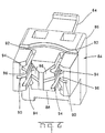
- the box 22 is a rectangular shell having a forward opening 24, a rear end 26 and a cable exit 28.
- the forward end includes latches 30 for retaining an insert 32 therein.
- the insert 32 includes a PCB 34 having a rear end 36 formed as a card edge with multiple conductors 38 thereupon.
- a connector 40 is incorporated onto the PCB 34.
- this connector 40 is a modular jack receptacle and provides an interface 42 for receiving a modular jack plug (not shown).
- the interface 42 is surrounded by a bezel 44 that includes latch arms 46 to engage latches 30 in box 22 when the insert 32 is placed within the box 22.
- a rear cover 48 is provided to close the rear end 26 of the box 22 once the connector 12 is mounted therein.
- the rear cover 48 includes a tab 50 that is received within the slot 28 of box 22 when the cover 48 is affixed thereto.
- the tab 50 in cooperation with the edges of the slot 28, engages the cable 4 to provide strain relief and possibly grounding of any general shielding of the cable 4 to the box 22.
- the electrical connector 12 according to the present invention is shown mounted within the box 22.
- the box 22 includes a mounting wall 52 which is engaged by the latch 20 for retaining the connector 12 therein.
- the connector box 22 is conductive, either by having been formed from a conductive material or a metallized plastic, and the connector 12 is also advantageously formed of conductive material, such as metallized plastic, by placing the connector 12 within the box 22, the connector 12 will be electrically commoned thereto. This will have further advantageous effects.
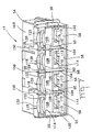
- the electrical connector 12 incorporates a main housing 14.
- the main housing 14 has a mating side 54 which in this example includes the card receiving slot 16 ( Figure 1). It is important to note that while the present invention can be advantageously used in a card-edge connector style, that the invention should not be limited.
- the main housing 14 also includes an open cable side 56 that is divided into a plurality of compartments 58 by partitions 60.
- the main housing 14 will be formed from a conductive material or metallized plastic.
- a plurality of contact carrying modules 62 are constructed to be received within compartments 58.
- the contact carrying modules 62 include opposing latches 64 so that they can be snapped in place within the main housing 14.
- the contact carrying module 62 is advantageously formed of insulative material although selective metallization could be used if desired.
- Each contact carrying module 62 includes two contacts 66 that are best seen and described in Figures 4 and 5. These contacts 66 include a mating end and a wire termination end 70.
- the connector 12 further includes a rear cover 18 that is fittable to the main housing 14 by a pair of latch arms 72 designed to engage corresponding catches 74 upon the main housing 14.
- the cover 18 further includes multiple U-shaped cable tabs 76. It is also envisioned that tabs 76 may be omitted.
- the rear cover 18 will also be manufactured from a conductive material or advantageously a metallized plastic.
- the contact 66 includes a mating end 68 that, in this embodiment, is a resilient tongue for engaging the conductive pads 38 of the card edge 36. Various configurations of this mating end 68 may be realized depending on the interface desired.
- the contact 66 further includes a cable termination end 70 that is formed as an insulation displacement contact (IDC).
- the IDC includes a wire receiving slot 78 for receiving an insulated wire and making connection thereto, as is well known in the industry.
- the wire termination end 70 could take on various other configurations, such as a crimp connection or a solder termination.
- a body section 80 is located between the mating end 68 and the wire termination end 70.
- the body portion 80 includes a retention lance 82 for incorporating the contact 66 into the contact carrying module 62.
- Various materials may be used for the contact 66 as desired and it may be advantageous to include a precious metal contact patch 84 for engaging the conductive pads 38 of the card edge 36.
- guide slots 94 that extend into the module 84 basically parallel to the contact receiving passageways 90. These guide slots 94, along with large chamfers 96 on both sides of the wire receiving slots 92, are useful for stabilizing a wire termination tool (not shown) that would be used to stuff the insulated wires into the IDC contact slot 70 of the contact 66 in a manner well known in industry.
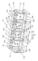
- the open cable side 56 of the main housing 14 is shell-like and defined by a lower wall 98, opposing side walls 100, 102 and upper wall 103.
- This shell-like open cable side 56 is further divided into a row of compartments 58 by partitions 60 that extend between the lower wall 98 and the upper wall 103.
- the partitions 60 are formed as tongues having a chamfered surface 104 extending on a side thereof to an end 106 of the tongue 60.
- the end 106 of tongue 60 is slightly recessed from the open cable side 56 of the connector 14.
- Each compartment 58 further includes a table 108 having an inverted, U-shaped, end 110 defining a passageway 112 thereunder and a passageway 114 thereover.
- the passageway 114 extends through the housing 14 to the mating side 54 while the passageway 112 exposes a latch 116 for retaining the contact carrying module 62.
- the table 108 is used to position the contact module 62 within the main housing 14.
- the end cover 18 that is constructed to close the open cable side 56 of the main housing 14 will be described in greater detail.
- the end cover 18 includes latches 72 to engage the catches 30 of the main housing in order to fix the cover 18 to the main housing 14.
- the cover 18 includes a body portion 124 having a rearward side 126 and a connector side 128. An interior surface 130 of the rearward side 126 faces the connector side 128.
- a trough-like structure is formed.
- the trough-like structure is further divided into compartments 58A by second partitions 60A that correspond to the partitions 60 of the main housing 14, as will be described below with reference to Figures 11 and 12.
- the second partition 60A also include chamfers 104A that extend along sides of the partition 60A to ends 142. It is important to note that at least a portion of the chamfer 104A of the partition 60A extends beyond the connector surface 128 in order to provide the ends 142 of the partition 60 with some flexibility. In this particular embodiment, the second partition 60A itself extends a small distance 144 beyond the connector edge 128. Further, the end 142 of the partitions extends upwards to a ledge 146 such that the second partitions 60A would be received between the lower wall 98 and the upper wall 103 of the main housing 14 when the cover 18 is fitted thereto.
- the cover 18 would be manufactured from a conductive material or a metallized plastic mold.
- a portion 148 of the partition 60A extends above the ledge 146 to be received within slots 150 formed in the upper wall 103 of the main housing 14 that correspond to the partition 60 therein.
- a plurality of U-shaped tabs 76 located along the upper wall 140 of the cover 18 are a plurality of U-shaped tabs 76 constructed to be received within the troughs 122 of the main housing 14. These legs of the U-shaped tabs 76 may take on various lengths as desired and provide some strain relief for the twisted-pair wire 6 and discontinuity in any pathway. As mentioned above, these tabs 76 are optional.
- a second saddle portion 152 At the base of the U-shaped tab 76 is a second saddle portion 152 that will be disposed opposite the first saddle portion 118 in the main housing 14.
- the electrical connector 12 is shown in assembled form.
- the contact carrying module 62 with the contact 66 is fitted to the housing 14 by the latch members 64 engaging corresponding latches 116 formed in the main housing 14.
- the contact 66 extends through the contact carrying passageway 90 such that the mating end 68 is disposed in the card edge receiving slot 16 on the mating end 54 of the main housing 14.
- the contact 66 is retained therein by the locking lance 82 that is received in a recess 156 of the body 84 in order to further retain the contact 66.
- a staking operation can be performed that utilizes the recess 158 above the contact lance 82 prior to assembling of the module 62 with the main housing 14 to further assure contact retention.
- the main housing has been assembled to the extent shown in Figure 9.
- a wire exit 160 is defined by the two saddle portions 120, 152 of the main housing 14 and cover 18 respectively for each of the compartments 58.
- This wire exit 160 is configured to be slightly smaller than that of the wires exiting such that an interference will exist. This interference is advantageously taken advantage of by allowing the shielding 10 that surrounds the wires 8 to extend into the compartment and be terminated only slightly above the rear IDC portion 88 of the contact module 62 when the various conductors 6 are being terminated.
- what is realized from the present invention is a structure that continues the shielding 10 provided to the twisted pair of wires 8 to a compartment 58 within a connector 12 such that a fully shielded twisted-pair interconnection is provided, thereby greatly reducing the effect of cross-talk from adjacent signal conductors 6 and any spurious electro-magnetic fields.
Landscapes
- Details Of Connecting Devices For Male And Female Coupling (AREA)
- Coupling Device And Connection With Printed Circuit (AREA)
- Multi-Conductor Connections (AREA)
Priority Applications (1)
| Application Number | Priority Date | Filing Date | Title |
|---|---|---|---|
| EP20010104117 EP1128488B1 (de) | 2000-02-21 | 2001-02-21 | Elektrischer Steckverbinder für Signalübertragung mit hoher Geschwindigkeit |
Applications Claiming Priority (3)
| Application Number | Priority Date | Filing Date | Title |
|---|---|---|---|
| EP00103625 | 2000-02-21 | ||
| EP00103625 | 2000-02-21 | ||
| EP20010104117 EP1128488B1 (de) | 2000-02-21 | 2001-02-21 | Elektrischer Steckverbinder für Signalübertragung mit hoher Geschwindigkeit |
Publications (3)
| Publication Number | Publication Date |
|---|---|
| EP1128488A2 true EP1128488A2 (de) | 2001-08-29 |
| EP1128488A3 EP1128488A3 (de) | 2013-07-31 |
| EP1128488B1 EP1128488B1 (de) | 2015-02-11 |
Family
ID=26070576
Family Applications (1)
| Application Number | Title | Priority Date | Filing Date |
|---|---|---|---|
| EP20010104117 Expired - Lifetime EP1128488B1 (de) | 2000-02-21 | 2001-02-21 | Elektrischer Steckverbinder für Signalübertragung mit hoher Geschwindigkeit |
Country Status (1)
| Country | Link |
|---|---|
| EP (1) | EP1128488B1 (de) |
Cited By (7)
| Publication number | Priority date | Publication date | Assignee | Title |
|---|---|---|---|---|
| EP1531523A3 (de) * | 2003-11-13 | 2006-03-01 | Tyco Electronics AMP GmbH | Anschlussklemme für Schaltungskarte |
| US7033219B2 (en) | 2004-06-10 | 2006-04-25 | Commscope Solutions Properties, Llc | Modular plug assemblies, terminated cable assemblies and methods for forming the same |
| WO2005124940A3 (en) * | 2004-06-10 | 2006-05-04 | Commscope Solutions Properties | Shielded jack assemblies and methods for forming a cable termination |
| WO2006065972A1 (en) * | 2004-12-17 | 2006-06-22 | Panduit Corp. | Systems for reducing crosstalk between communications connectors |
| US7221138B2 (en) | 2005-09-27 | 2007-05-22 | Saifun Semiconductors Ltd | Method and apparatus for measuring charge pump output current |
| CN100539323C (zh) * | 2004-06-10 | 2009-09-09 | 北卡罗来纳科姆斯科普公司 | 插座组件和用于制作该插座组件的方法 |
| WO2011003914A1 (en) * | 2009-07-08 | 2011-01-13 | Tyco Electronics Amp Gmbh | Electrical plug connector having a one-piece connector housing and assembly method |
Citations (4)
| Publication number | Priority date | Publication date | Assignee | Title |
|---|---|---|---|---|
| EP0274487A1 (de) | 1986-06-13 | 1988-07-20 | Amp Inc | Schnittstelle für lokales netz. |
| EP0525703A1 (de) | 1991-08-01 | 1993-02-03 | Siemens Aktiengesellschaft | Steckverbindung für Computernetze im Hausbereich |
| US5186647A (en) | 1992-02-24 | 1993-02-16 | At&T Bell Laboratories | High frequency electrical connector |
| US5484308A (en) | 1993-04-29 | 1996-01-16 | The Whitaker Corporation | Data communications outlet kit |
Family Cites Families (2)
| Publication number | Priority date | Publication date | Assignee | Title |
|---|---|---|---|---|
| US5605469A (en) * | 1995-01-05 | 1997-02-25 | Thomas & Betts Corporation | Electrical connector having an improved conductor holding block and conductor shield |
| EP0809331B1 (de) * | 1996-05-23 | 1999-06-16 | BKS Kabel-Service AG | Mehrpoliges Steckersystem mit einer Steckdose und mindestens einem Stecker zum elektrischen und mechanischen Verbinden von elektrischen Leitern |
-
2001
- 2001-02-21 EP EP20010104117 patent/EP1128488B1/de not_active Expired - Lifetime
Patent Citations (4)
| Publication number | Priority date | Publication date | Assignee | Title |
|---|---|---|---|---|
| EP0274487A1 (de) | 1986-06-13 | 1988-07-20 | Amp Inc | Schnittstelle für lokales netz. |
| EP0525703A1 (de) | 1991-08-01 | 1993-02-03 | Siemens Aktiengesellschaft | Steckverbindung für Computernetze im Hausbereich |
| US5186647A (en) | 1992-02-24 | 1993-02-16 | At&T Bell Laboratories | High frequency electrical connector |
| US5484308A (en) | 1993-04-29 | 1996-01-16 | The Whitaker Corporation | Data communications outlet kit |
Cited By (13)
| Publication number | Priority date | Publication date | Assignee | Title |
|---|---|---|---|---|
| EP1531523A3 (de) * | 2003-11-13 | 2006-03-01 | Tyco Electronics AMP GmbH | Anschlussklemme für Schaltungskarte |
| US7134904B2 (en) | 2003-11-13 | 2006-11-14 | Tyco Electronics Amp Gmbh | Terminal unit for putting a lead into contact with a printed circuit board |
| AU2005255867B2 (en) * | 2004-06-10 | 2010-05-20 | Commscope, Inc. Of North Carolina | Shielded jack assemblies and methods for forming a cable termination |
| US7033219B2 (en) | 2004-06-10 | 2006-04-25 | Commscope Solutions Properties, Llc | Modular plug assemblies, terminated cable assemblies and methods for forming the same |
| WO2005124940A3 (en) * | 2004-06-10 | 2006-05-04 | Commscope Solutions Properties | Shielded jack assemblies and methods for forming a cable termination |
| US7083472B2 (en) | 2004-06-10 | 2006-08-01 | Commscope Solutions Properties, Llc | Shielded jack assemblies and methods for forming a cable termination |
| AU2005255867C1 (en) * | 2004-06-10 | 2010-10-14 | Commscope, Inc. Of North Carolina | Shielded jack assemblies and methods for forming a cable termination |
| US7249974B2 (en) | 2004-06-10 | 2007-07-31 | Commscope, Inc. Of North Carolina | Shielded jack assemblies and methods for forming a cable termination |
| US7510439B2 (en) | 2004-06-10 | 2009-03-31 | Commscope, Inc. Of North Carolina | Shielded jack assemblies and methods for forming a cable termination |
| CN100539323C (zh) * | 2004-06-10 | 2009-09-09 | 北卡罗来纳科姆斯科普公司 | 插座组件和用于制作该插座组件的方法 |
| WO2006065972A1 (en) * | 2004-12-17 | 2006-06-22 | Panduit Corp. | Systems for reducing crosstalk between communications connectors |
| US7221138B2 (en) | 2005-09-27 | 2007-05-22 | Saifun Semiconductors Ltd | Method and apparatus for measuring charge pump output current |
| WO2011003914A1 (en) * | 2009-07-08 | 2011-01-13 | Tyco Electronics Amp Gmbh | Electrical plug connector having a one-piece connector housing and assembly method |
Also Published As
| Publication number | Publication date |
|---|---|
| EP1128488A3 (de) | 2013-07-31 |
| EP1128488B1 (de) | 2015-02-11 |
Similar Documents
| Publication | Publication Date | Title |
|---|---|---|
| US6394844B1 (en) | Electrical connector for high speed signal transmission | |
| USRE38519E1 (en) | Low crosstalk modular communication connector | |
| US6705902B1 (en) | Connector assembly having contacts with uniform electrical property of resistance | |
| EP0992084B1 (de) | Abgeschirmter kabelstecker | |
| EP0080772B1 (de) | Elektrischer Zusammenbau eines Steckers und einer Steckdose | |
| EP0460976B1 (de) | Steckverbinder mit Erdungsstruktur | |
| EP0658953B1 (de) | Anordnung von modularen Steckern mit einer Mehrzahl von Öffnungen | |
| US6582255B2 (en) | High-density plug connector for twisted pair cable | |
| US6478610B1 (en) | Electrical connector assembly | |
| EP1923970A2 (de) | Stecker für eine modulare Kommunikation mit geringem Übersprechen | |
| EP1450442A2 (de) | Verbindungsvorrichtung | |
| EP0460975A1 (de) | Steckverbinder mit Erdungsstruktur | |
| US4863393A (en) | Modular jack assembly with improved bridging arrangement | |
| US11239617B2 (en) | Cable receptacle connector | |
| EP0614248B1 (de) | Schnittstelle für ein lokales Netz (LAN) | |
| US12327948B2 (en) | High density coupling panel | |
| US5151036A (en) | Connectors with ground structure | |
| US5141453A (en) | Connectors with ground structure | |
| US5261829A (en) | Connectors with ground structure | |
| US6184460B1 (en) | Modular box shield for forming a coaxial header | |
| US6887094B2 (en) | Shielded connection arrangement for data transfer | |
| EP1128488B1 (de) | Elektrischer Steckverbinder für Signalübertragung mit hoher Geschwindigkeit | |
| US6375506B1 (en) | High-density high-speed input/output connector | |
| US20240347982A1 (en) | Cable card assembly of an electrical connector having capacitors | |
| GB2428337A (en) | Enhanced jack with plug engaging printed circuit board |
Legal Events
| Date | Code | Title | Description |
|---|---|---|---|
| PUAI | Public reference made under article 153(3) epc to a published international application that has entered the european phase |
Free format text: ORIGINAL CODE: 0009012 |
|
| AK | Designated contracting states |
Kind code of ref document: A2 Designated state(s): AT BE CH CY DE DK ES FI FR GB GR IE IT LI LU MC NL PT SE TR |
|
| AX | Request for extension of the european patent |
Free format text: AL;LT;LV;MK;RO;SI |
|
| PUAL | Search report despatched |
Free format text: ORIGINAL CODE: 0009013 |
|
| AK | Designated contracting states |
Kind code of ref document: A3 Designated state(s): AT BE CH CY DE DK ES FI FR GB GR IE IT LI LU MC NL PT SE TR |
|
| AX | Request for extension of the european patent |
Extension state: AL LT LV MK RO SI |
|
| RIC1 | Information provided on ipc code assigned before grant |
Ipc: H01R 13/658 20110101AFI20130627BHEP |
|
| RAP1 | Party data changed (applicant data changed or rights of an application transferred) |
Owner name: TYCO ELECTRONICS AMP ESPANA S.A. |
|
| 17P | Request for examination filed |
Effective date: 20140121 |
|
| RBV | Designated contracting states (corrected) |
Designated state(s): AT BE CH CY DE DK ES FI FR GB GR IE IT LI LU MC NL PT SE TR |
|
| AKX | Designation fees paid |
Designated state(s): AT BE CH CY DE DK ES FI FR GB GR IE IT LI LU MC NL PT SE TR |
|
| 17Q | First examination report despatched |
Effective date: 20140319 |
|
| GRAP | Despatch of communication of intention to grant a patent |
Free format text: ORIGINAL CODE: EPIDOSNIGR1 |
|
| INTG | Intention to grant announced |
Effective date: 20140819 |
|
| GRAS | Grant fee paid |
Free format text: ORIGINAL CODE: EPIDOSNIGR3 |
|
| GRAA | (expected) grant |
Free format text: ORIGINAL CODE: 0009210 |
|
| AK | Designated contracting states |
Kind code of ref document: B1 Designated state(s): AT BE CH CY DE DK ES FI FR GB GR IE IT LI LU MC NL PT SE TR |
|
| REG | Reference to a national code |
Ref country code: GB Ref legal event code: FG4D |
|
| REG | Reference to a national code |
Ref country code: CH Ref legal event code: EP |
|
| REG | Reference to a national code |
Ref country code: IE Ref legal event code: FG4D |
|
| REG | Reference to a national code |
Ref country code: CH Ref legal event code: NV Representative=s name: MURGITROYD AND COMPANY, CH |
|
| REG | Reference to a national code |
Ref country code: AT Ref legal event code: REF Ref document number: 710177 Country of ref document: AT Kind code of ref document: T Effective date: 20150315 |
|
| REG | Reference to a national code |
Ref country code: DE Ref legal event code: R096 Ref document number: 60149230 Country of ref document: DE Effective date: 20150326 |
|
| REG | Reference to a national code |
Ref country code: NL Ref legal event code: VDEP Effective date: 20150211 |
|
| PG25 | Lapsed in a contracting state [announced via postgrant information from national office to epo] |
Ref country code: BE Free format text: LAPSE BECAUSE OF NON-PAYMENT OF DUE FEES Effective date: 20150228 |
|
| PG25 | Lapsed in a contracting state [announced via postgrant information from national office to epo] |
Ref country code: SE Free format text: LAPSE BECAUSE OF FAILURE TO SUBMIT A TRANSLATION OF THE DESCRIPTION OR TO PAY THE FEE WITHIN THE PRESCRIBED TIME-LIMIT Effective date: 20150211 Ref country code: ES Free format text: LAPSE BECAUSE OF FAILURE TO SUBMIT A TRANSLATION OF THE DESCRIPTION OR TO PAY THE FEE WITHIN THE PRESCRIBED TIME-LIMIT Effective date: 20150211 Ref country code: FI Free format text: LAPSE BECAUSE OF FAILURE TO SUBMIT A TRANSLATION OF THE DESCRIPTION OR TO PAY THE FEE WITHIN THE PRESCRIBED TIME-LIMIT Effective date: 20150211 |
|
| PG25 | Lapsed in a contracting state [announced via postgrant information from national office to epo] |
Ref country code: GR Free format text: LAPSE BECAUSE OF FAILURE TO SUBMIT A TRANSLATION OF THE DESCRIPTION OR TO PAY THE FEE WITHIN THE PRESCRIBED TIME-LIMIT Effective date: 20150512 Ref country code: NL Free format text: LAPSE BECAUSE OF FAILURE TO SUBMIT A TRANSLATION OF THE DESCRIPTION OR TO PAY THE FEE WITHIN THE PRESCRIBED TIME-LIMIT Effective date: 20150211 |
|
| PG25 | Lapsed in a contracting state [announced via postgrant information from national office to epo] |
Ref country code: DK Free format text: LAPSE BECAUSE OF FAILURE TO SUBMIT A TRANSLATION OF THE DESCRIPTION OR TO PAY THE FEE WITHIN THE PRESCRIBED TIME-LIMIT Effective date: 20150211 |
|
| REG | Reference to a national code |
Ref country code: DE Ref legal event code: R097 Ref document number: 60149230 Country of ref document: DE |
|
| REG | Reference to a national code |
Ref country code: IE Ref legal event code: MM4A |
|
| PG25 | Lapsed in a contracting state [announced via postgrant information from national office to epo] |
Ref country code: MC Free format text: LAPSE BECAUSE OF FAILURE TO SUBMIT A TRANSLATION OF THE DESCRIPTION OR TO PAY THE FEE WITHIN THE PRESCRIBED TIME-LIMIT Effective date: 20150211 |
|
| PLBE | No opposition filed within time limit |
Free format text: ORIGINAL CODE: 0009261 |
|
| STAA | Information on the status of an ep patent application or granted ep patent |
Free format text: STATUS: NO OPPOSITION FILED WITHIN TIME LIMIT |
|
| PG25 | Lapsed in a contracting state [announced via postgrant information from national office to epo] |
Ref country code: IT Free format text: LAPSE BECAUSE OF FAILURE TO SUBMIT A TRANSLATION OF THE DESCRIPTION OR TO PAY THE FEE WITHIN THE PRESCRIBED TIME-LIMIT Effective date: 20150211 |
|
| 26N | No opposition filed |
Effective date: 20151112 |
|
| GBPC | Gb: european patent ceased through non-payment of renewal fee |
Effective date: 20150511 |
|
| PG25 | Lapsed in a contracting state [announced via postgrant information from national office to epo] |
Ref country code: IE Free format text: LAPSE BECAUSE OF NON-PAYMENT OF DUE FEES Effective date: 20150221 |
|
| REG | Reference to a national code |
Ref country code: FR Ref legal event code: PLFP Year of fee payment: 16 |
|
| REG | Reference to a national code |
Ref country code: AT Ref legal event code: UEP Ref document number: 710177 Country of ref document: AT Kind code of ref document: T Effective date: 20150211 |
|
| PG25 | Lapsed in a contracting state [announced via postgrant information from national office to epo] |
Ref country code: GB Free format text: LAPSE BECAUSE OF NON-PAYMENT OF DUE FEES Effective date: 20150511 |
|
| PG25 | Lapsed in a contracting state [announced via postgrant information from national office to epo] |
Ref country code: BE Free format text: LAPSE BECAUSE OF FAILURE TO SUBMIT A TRANSLATION OF THE DESCRIPTION OR TO PAY THE FEE WITHIN THE PRESCRIBED TIME-LIMIT Effective date: 20150211 |
|
| REG | Reference to a national code |
Ref country code: FR Ref legal event code: PLFP Year of fee payment: 17 |
|
| PG25 | Lapsed in a contracting state [announced via postgrant information from national office to epo] |
Ref country code: CY Free format text: LAPSE BECAUSE OF FAILURE TO SUBMIT A TRANSLATION OF THE DESCRIPTION OR TO PAY THE FEE WITHIN THE PRESCRIBED TIME-LIMIT Effective date: 20150211 |
|
| PG25 | Lapsed in a contracting state [announced via postgrant information from national office to epo] |
Ref country code: PT Free format text: LAPSE BECAUSE OF FAILURE TO SUBMIT A TRANSLATION OF THE DESCRIPTION OR TO PAY THE FEE WITHIN THE PRESCRIBED TIME-LIMIT Effective date: 20150611 |
|
| PG25 | Lapsed in a contracting state [announced via postgrant information from national office to epo] |
Ref country code: TR Free format text: LAPSE BECAUSE OF FAILURE TO SUBMIT A TRANSLATION OF THE DESCRIPTION OR TO PAY THE FEE WITHIN THE PRESCRIBED TIME-LIMIT Effective date: 20150211 |
|
| PG25 | Lapsed in a contracting state [announced via postgrant information from national office to epo] |
Ref country code: LU Free format text: LAPSE BECAUSE OF NON-PAYMENT OF DUE FEES Effective date: 20150221 |
|
| REG | Reference to a national code |
Ref country code: FR Ref legal event code: PLFP Year of fee payment: 18 |
|
| PGFP | Annual fee paid to national office [announced via postgrant information from national office to epo] |
Ref country code: DE Payment date: 20200227 Year of fee payment: 20 |
|
| PGFP | Annual fee paid to national office [announced via postgrant information from national office to epo] |
Ref country code: FR Payment date: 20200225 Year of fee payment: 20 |
|
| REG | Reference to a national code |
Ref country code: CH Ref legal event code: PL |
|
| REG | Reference to a national code |
Ref country code: AT Ref legal event code: MM01 Ref document number: 710177 Country of ref document: AT Kind code of ref document: T Effective date: 20200221 |
|
| PG25 | Lapsed in a contracting state [announced via postgrant information from national office to epo] |
Ref country code: CH Free format text: LAPSE BECAUSE OF NON-PAYMENT OF DUE FEES Effective date: 20200229 Ref country code: LI Free format text: LAPSE BECAUSE OF NON-PAYMENT OF DUE FEES Effective date: 20200229 Ref country code: AT Free format text: LAPSE BECAUSE OF NON-PAYMENT OF DUE FEES Effective date: 20200221 |
|
| REG | Reference to a national code |
Ref country code: DE Ref legal event code: R071 Ref document number: 60149230 Country of ref document: DE |