EP1128582A1 - Regenerator für wellenlängenmultiplexierte Übertragungssysteme - Google Patents
Regenerator für wellenlängenmultiplexierte Übertragungssysteme Download PDFInfo
- Publication number
- EP1128582A1 EP1128582A1 EP01400139A EP01400139A EP1128582A1 EP 1128582 A1 EP1128582 A1 EP 1128582A1 EP 01400139 A EP01400139 A EP 01400139A EP 01400139 A EP01400139 A EP 01400139A EP 1128582 A1 EP1128582 A1 EP 1128582A1
- Authority
- EP
- European Patent Office
- Prior art keywords
- regenerator
- signals
- clock
- voltage
- modulators
- Prior art date
- Legal status (The legal status is an assumption and is not a legal conclusion. Google has not performed a legal analysis and makes no representation as to the accuracy of the status listed.)
- Withdrawn
Links
- 230000005540 biological transmission Effects 0.000 title claims abstract description 20
- 230000003287 optical effect Effects 0.000 claims abstract description 9
- 238000011084 recovery Methods 0.000 claims description 9
- 239000013307 optical fiber Substances 0.000 abstract description 5
- 230000001360 synchronised effect Effects 0.000 description 17
- 230000008929 regeneration Effects 0.000 description 9
- 238000011069 regeneration method Methods 0.000 description 9
- 239000000835 fiber Substances 0.000 description 4
- 238000013459 approach Methods 0.000 description 3
- 230000001934 delay Effects 0.000 description 3
- 239000006185 dispersion Substances 0.000 description 3
- 238000005516 engineering process Methods 0.000 description 2
- 238000001914 filtration Methods 0.000 description 2
- 230000010363 phase shift Effects 0.000 description 2
- 230000001172 regenerating effect Effects 0.000 description 2
- 229910008310 Si—Ge Inorganic materials 0.000 description 1
- 230000032683 aging Effects 0.000 description 1
- 230000015556 catabolic process Effects 0.000 description 1
- 230000008878 coupling Effects 0.000 description 1
- 238000010168 coupling process Methods 0.000 description 1
- 238000005859 coupling reaction Methods 0.000 description 1
- 230000000694 effects Effects 0.000 description 1
- 230000001939 inductive effect Effects 0.000 description 1
- 238000009434 installation Methods 0.000 description 1
- 238000000034 method Methods 0.000 description 1
- 230000000737 periodic effect Effects 0.000 description 1
- 230000035945 sensitivity Effects 0.000 description 1
- 238000011144 upstream manufacturing Methods 0.000 description 1
Images
Classifications
-
- H—ELECTRICITY
- H04—ELECTRIC COMMUNICATION TECHNIQUE
- H04B—TRANSMISSION
- H04B10/00—Transmission systems employing electromagnetic waves other than radio-waves, e.g. infrared, visible or ultraviolet light, or employing corpuscular radiation, e.g. quantum communication
- H04B10/29—Repeaters
- H04B10/291—Repeaters in which processing or amplification is carried out without conversion of the main signal from optical form
- H04B10/299—Signal waveform processing, e.g. reshaping or retiming
-
- H—ELECTRICITY
- H04—ELECTRIC COMMUNICATION TECHNIQUE
- H04J—MULTIPLEX COMMUNICATION
- H04J14/00—Optical multiplex systems
- H04J14/02—Wavelength-division multiplex systems
- H04J14/03—WDM arrangements
- H04J14/0305—WDM arrangements in end terminals
-
- H—ELECTRICITY
- H04—ELECTRIC COMMUNICATION TECHNIQUE
- H04B—TRANSMISSION
- H04B2210/00—Indexing scheme relating to optical transmission systems
- H04B2210/25—Distortion or dispersion compensation
- H04B2210/258—Distortion or dispersion compensation treating each wavelength or wavelength band separately
-
- H—ELECTRICITY
- H04—ELECTRIC COMMUNICATION TECHNIQUE
- H04L—TRANSMISSION OF DIGITAL INFORMATION, e.g. TELEGRAPHIC COMMUNICATION
- H04L7/00—Arrangements for synchronising receiver with transmitter
- H04L7/0075—Arrangements for synchronising receiver with transmitter with photonic or optical means
Definitions
- the invention relates to optical fiber transmission systems using wavelength multiplexing, and more specifically, signal regeneration by optical modulation in such transmission systems.
- a first solution to this problem consists in proceeding to separate the different channels before proceeding for each channel to regeneration by synchronous modulation.
- the regenerated channels can then be multiplexed.
- a regenerator in this configuration is made up of as many modulators synchronous that there are channels, mounted in parallel; each regenerator present its own clock recovery circuit - due to the lack of synchronicity of the canals.
- This solution is bulky, expensive and consumes power important, because of the number of electronic circuits to be replicated for the clock recovery.
- the French patent application filed on 19.02.99 under the number 99 02 126 proposes to regenerate in a regenerator only a subset channels - for example one in four channels. All channels are processed after several regenerators - four in the example. This solution reduces the number of modulators to be connected in parallel in each regenerator - from one factor four in the example. For equal performances, the total number of modulators in the transmission system remains the same; this solution simplifies the structure of a regenerator, but does not affect cost or power consumed.
- This article proposes to allocate wavelengths to the different channels of the multiplex so that, for given intervals Z R between the repeaters, the signals of the different channels, or more exactly the bit times of the different channels of the multiplex, are substantially synchronized when arriving at repeaters.
- This multiplex wavelength allocation technique is also described in French patent application FR-A-2,743,964 in the name of Alcatel Submarine Networks. In this article, it is proposed to choose a subgroup of channels, synchronous not only at intervals Z R , but also at intervals under multiples of Z R.
- FR-A-2 770 001 proposes to use a synchronous modulator to modulate soliton signals of all channels in a multiplex transmission system in wavelength at a frequency N / T multiple of the clock frequency of 1 / T signals. In this way we can relax the constraint of synchronicity, by imposing no longer a bit time synchronicity, but a synchronicity of the different channels at a sub multiple of the bit time.
- FR-A-2 759 516 proposes to demultiplex the different channels, and their apply the delays necessary to resynchronize them, After multiplexing, the different channels can be modulated using a single optical modulator.
- the French patent application filed under number 97 06 590 proposes to use a chain of networks formed in a fiber to apply suitable delays, and resynchronize the different channels without having to demultiplex and remultiplexing.
- DCF compensation dispersion fiber
- the invention provides a solution to the problem of regenerating the channels.
- wavelength division multiplex transmission systems She allows to reduce the cost and power consumed by regenerators, without, however, impose a constraint on the choice of wavelengths.
- the invention proposes a regenerator for a wavelength division multiplex transmission system, comprising a demultiplexer for separating the signals from different channels, a plurality of optical modulators each receiving signals from the demultiplexer and a modulation clock B i coming from a clock distribution unit, and a multiplexer combining the signals modulated by said modulators;
- the clock distribution unit has a reference clock and, for each of the modulators, means for phasing a copy of the reference clock with the signals applied to the modulator.
- the phasing means comprise for each of the modulators a phase lock loop.
- the phase lock loop can advantageously include a phase shifter receiving a copy of the reference clock and providing a modulation clock, the phase shifter being controlled by function of the average power of the modulator output signals.
- the phase lock loop preferably includes a coupler taking part of the modulator output signals and a receiving photodiode the signals coming from the coupler and providing a voltage representative of the average power of the modulator output signals.
- the phase shifter is advantageously controlled by a signal C i which is a function of the difference between said voltage and a reference voltage V REF .
- the reference voltage can be a function of the total power of the signals at the regenerator outlet, or can be controlled remotely.
- the reference clock is supplied by a voltage controlled oscillator. It can in particular be ordered depending on the signals applied to the regenerator.
- the regenerator has a coupler taking part of the regenerator input signals, a circuit clock recovery receiving signals picked up by the coupler and providing at output an oscillator control signal
- the invention finally relates to a multiplex transmission system in wavelength, including such a regenerator.
- the invention proposes, in order to reduce the volume, the cost and the complexity of regenerators, to share between the synchronous modulators a distribution unit of common clocks.
- the clock distribution unit has a clock reference, which is replicated in as many copies as necessary; each copy is phasing with a channel.
- Phase locked loop can be used to phase the copies of the reference clock and the channels correspondents.
- An embodiment of a regenerative, in a four-channel transmission system is not of course not limited to this number of channels.
- the four channels are modulated separately; the invention applies equally to the case described in Mr. Nakazawa's article, where some of the channels are modulated by the same modulator.
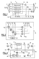
- FIG. 1 shows a schematic representation of a regenerator according to the invention
- the regenerator has a demultiplexer 2, which receives the multiplexed signals from the different channels as input, and outputs the separate channels.
- the channels supplied at the output of the multiplexer are applied to a set of optical modulators.
- the different modulators can be grouped together on the same InP chip 4.
- This chip has clock inputs 6 for receiving the clocks intended to modulate the different channels, inputs 8 for receiving the signals of the separate channels coming from the demultiplexer 2, and from the outputs 10 supplying the signals of the different channels modulated by the clocks.
- At the output of the modulators are provided on each of the channels a coupler 12 i , which takes part of the modulated signal.
- the modulated signals are then combined in a multiplexer 14.
- the regenerator also has a clock distribution unit 16, which receives the signals A i taken from the modulator output on each channel, and which supplies clocks B i intended for each modulator.
- the clock B i for a channel ⁇ i is obtained by locking in phase of a reference clock, from the signal taken at the modulator output for the channel in question.
- the operation of the regenerator of Figure 1 is as follows.
- the signals different channels are separated in multiplexer 2, are respectively modulated by the different modulators, then are recombined in the multiplexer 14.
- the clock distribution unit provides the clocks necessary for modulation; the operation of this unit appears in more detail below.
- the invention makes it possible to share the clock distribution unit, and avoids the multiplication of the circuits proposed in the regenerators of the state of the art.
- the regenerator also locks the modulation clocks to each of the channels, regardless of the phase variations of the different broadcast channels; the regenerator is also insensitive to variations in output power, in particular due to the location in the transmission, breakdowns or interruptions of transmission on the different channels.
- FIG. 2 shows a schematic representation of the clock distribution unit of the regenerator of FIG. 1.
- the distribution unit receives the signals A i taken downstream from the modulators and supplies clocks B i .
- the signals taken downstream from the modulators are supplied to low-frequency photodiodes 16 i ; these respectively supply a voltage representative of the average power of the modulated signal of each channel.
- low frequency is meant in the expression “low frequency photodiode” frequencies below the frequency of the transmitted signals.
- the photodiode can be a photodiode whose frequency response is limited to a few tens or hundreds of kHz; a photodiode therefore provides a signal therefore the power is representative of the average power of the modulated signal of a channel, over a window with a length of the order of a few tens of thousands or a few million bits.
- each of the photodiodes is applied to the non-inverting input of a low frequency amplifier 18 i , which is mounted as a comparator; the term "low frequency” in the expression “low frequency amplifier” means, as for the photodiode, that the frequency response of the amplifier is limited to a few tens or hundreds of kHz, for example.
- Each amplifier receives on its inverting input a reference voltage V REF , and outputs a voltage C i representative of the difference between the output voltage of the photodiode and the reference voltage.
- each amplifier 18 i is applied to a control input of a phase controller 20 i or phase shifter referenced ⁇ i in the figure.
- phase controllers or phase shifters are commercially available or can be produced by generic electronic circuits of various types, ie analog / digital, hybrid / integrated, etc.
- Each phase controller also receives a reference clock, and outputs a clock B i derived from the reference clock, the phase of which is a function of the voltage applied to its control input.
- the reference clock is provided by a voltage controlled oscillator (VCO) 22.
- the clock is set to the frequency of the signals transmitted on each channel - 10 GHz in the example.
- the reference clock can be set by varying the voltage applied to the oscillator, during installation or during operation;
- Figure 3 also shows a clock recovery circuit for adjusting the voltage applied to the oscillator.
- the operation of the clock generation unit in FIG. 2 is as follows: the phase of the reference clock applied to each phase controller 20 i is adjusted in the phase locked loop formed by the phase controller 20 i , the modulator, the photodiode 16 i and the amplifier 18 i .
- the operation of the phase locked loop relies on the fact that the average power of the modulated signal is maximum when the modulation clock B i is in phase with the signal.
- the output voltage of the photodiode 16 i varies between a minimum value - for a phase shift of ⁇ between the modulation clock and the signals to be modulated - and a maximum value when the modulation clock and the signals to be modulated are in phase .
- the ratio between the minimum value and the maximum value depends on the modulation depth chosen, a phase shift of ⁇ "crushing" the pulses by a value equal to the modulation depth.
- This maximum value depends on the proportion of "0" and “1” in the signals to be modulated and on the characteristics of the photodiodes, and as explained below, the reference voltage V REF preferably equal to this maximum value is chosen.
- the modulator output has an average power which is a function of the phase, and the output voltage of the photodiode is between a zero voltage and the reference voltage V REF . If the output voltage of the photodiode is zero, the differential voltage supplied by the amplifier 18 i is non-zero, and the phase controller 20 i therefore varies the phase of the clock B i .
- the phase of the clock B i approaches the phase of the signals to be modulated, the voltage supplied by the photodiode approaches the reference voltage V REF , and the control voltage applied to the phase controller 20 i s approach zero.
- the loop therefore has the effect of locking the phase of the clock B i on the phase of the signals to be modulated in the corresponding channel.
- the use of low frequency components - photodiodes and amplifiers differentials - helps limit the cost of the clock distribution unit the invention. You can actually use common electronic components, less expensive. In particular, it is not necessary in the embodiment of Figures 1 and 2 to have a high speed photodiode, i. e. likely to provide a signal varying appreciably with the frequency of the signals transmitted.
- the unit of clock distribution can be implemented on a single chip, by integrating components - photodiodes, amplifiers, phase controllers - according to a Si or Si-Ge technology.
- the reference voltage V REF is preferably equal to the maximum voltage supplied by the photodiode when the clock for the corresponding channel is in phase with the signals to be modulated. Small variations between the maximum voltage of the photodiodes and the reference voltage are however acceptable. Such deviations can also be corrected by generic control systems more complex than the solution proposed below, in particular in coupling with supervision signals; in such a case, the reference voltage could be controlled remotely, depending on the results of the supervision. This solution allows you to adjust the reference voltage according to power fluctuations or device imperfections.
- FIG. 3 shows a schematic representation of another embodiment of the clock distribution unit.
- the regenerator has a coupler 24, which takes a portion of the output from the multiplexer 14 modulated signals.
- the signals are applied to a low frequency photodiode 26 - of the kind of photodiodes 16 i , which supplies a voltage representative of the average power of the signals of the different channels.
- This voltage is applied to a voltage divider 28, which moreover receives a control voltage V C and outputs a voltage representative of the average power of the signals in a channel.
- the division ratio of the voltage divider 28 is a function of the number of channels.
- the control voltage V C can advantageously be adjusted remotely. It is thus possible to compensate remotely for variations in the number of channels, for example in the event of interruption of the transmission on the channel for repair or incident.
- FIG. 3 also shows an embodiment in which the regenerator also has clock recovery means.
- the regenerator has upstream of the demultiplexer 2 a coupler 30 for withdrawing part of the multiplexed signals.
- the sampled signals are supplied to a filter optics 32 which filters the signals of a reference channel.
- the filtered signals are applied to a clock recovery circuit 34.
- this circuit provides a signal representative of the clock frequency of the reference channel. This signal can be used to control the voltage controlled oscillator.
- the clock recovery circuit which could directly supply the reference clock, itself taking reference on a signal optics sampled in the multiplex.
- the regenerator of the invention applies to all transmission systems with wavelength multiplexing. It allows optical regeneration of channels, without implying the constraints of prior synchronization, nor inducing a multiplication of the components necessary to generate the different clocks modulation.
- the present invention is not limited to the examples and modes described and represented, but it is likely to be numerous variants accessible to those skilled in the art.
- some of the modulators or all of the modulators could modulate multiple canals.
- Other solutions can be used to generate the reference clock than a voltage controlled oscillator, for example a frequency oscillator fixed, or directly the output of a clock recovery circuit itself slaved on a reference channel extracted from the multiplex.
- a voltage controlled oscillator for example a frequency oscillator fixed, or directly the output of a clock recovery circuit itself slaved on a reference channel extracted from the multiplex.
- We did not represent either at the ' figure the elements such as filters or amplifiers which can be added in a regenerator.
Landscapes
- Engineering & Computer Science (AREA)
- Computer Networks & Wireless Communication (AREA)
- Signal Processing (AREA)
- Physics & Mathematics (AREA)
- Electromagnetism (AREA)
- Optical Communication System (AREA)
Applications Claiming Priority (2)
| Application Number | Priority Date | Filing Date | Title |
|---|---|---|---|
| FR0002089 | 2000-02-21 | ||
| FR0002089A FR2805417B1 (fr) | 2000-02-21 | 2000-02-21 | Regenerateur pour systeme de transmission a multiplexage en longueur d'onde |
Publications (1)
| Publication Number | Publication Date |
|---|---|
| EP1128582A1 true EP1128582A1 (de) | 2001-08-29 |
Family
ID=8847180
Family Applications (1)
| Application Number | Title | Priority Date | Filing Date |
|---|---|---|---|
| EP01400139A Withdrawn EP1128582A1 (de) | 2000-02-21 | 2001-01-18 | Regenerator für wellenlängenmultiplexierte Übertragungssysteme |
Country Status (4)
| Country | Link |
|---|---|
| US (1) | US6931213B2 (de) |
| EP (1) | EP1128582A1 (de) |
| JP (1) | JP2001268009A (de) |
| FR (1) | FR2805417B1 (de) |
Cited By (2)
| Publication number | Priority date | Publication date | Assignee | Title |
|---|---|---|---|---|
| WO2004054151A1 (fr) * | 2002-12-02 | 2004-06-24 | Ekinops | Procede de transmission synchrone longue distance par fibre optique |
| WO2008072945A1 (es) * | 2006-12-15 | 2008-06-19 | Instituto Tecnologico Y De Estudios Superiores De Monterrey | Regenerador de fase de señales ópticas para formatos de modulación diferencial con cambios de fase |
Families Citing this family (10)
| Publication number | Priority date | Publication date | Assignee | Title |
|---|---|---|---|---|
| US7483639B2 (en) * | 2001-05-10 | 2009-01-27 | Fujitsu Limited | Method and system for transmitting information in an optical communication system using distributed amplification |
| JP2003005140A (ja) * | 2001-06-19 | 2003-01-08 | Kddi Corp | 光信号再生装置 |
| US7171124B2 (en) * | 2001-07-19 | 2007-01-30 | Lucent Technologies Inc. | Wavelength routing and switching mechanism for a photonic transport network |
| FR2832571B1 (fr) * | 2001-11-22 | 2004-04-16 | Cit Alcatel | Systeme de transmission par fibres optiques a horloge commune |
| JP4625284B2 (ja) * | 2004-07-20 | 2011-02-02 | 株式会社日立製作所 | 光伝送装置 |
| JP4114687B2 (ja) * | 2005-09-01 | 2008-07-09 | 沖電気工業株式会社 | マルチレートクロック信号抽出方法及びマルチレートクロック信号抽出装置 |
| US7653092B2 (en) * | 2005-09-28 | 2010-01-26 | Electronics And Telecommunications Research Institute | Time-division multiplexing/demultiplexing system and method |
| GB0525234D0 (en) * | 2005-12-12 | 2006-01-18 | Qinetiq Ltd | Correlation apparatus |
| US9369207B2 (en) * | 2010-11-15 | 2016-06-14 | Alcatel Lucent | Apparatus and method for two-stage optical network |
| BR112021004133A8 (pt) * | 2018-11-05 | 2023-05-09 | Lyteloop Tech Llc | Sistemas e métodos para construir, operar e controlar múltiplos amplificadores, regeneradores e transceptores usando os componentes comuns compartilhados |
Citations (2)
| Publication number | Priority date | Publication date | Assignee | Title |
|---|---|---|---|---|
| US5864414A (en) * | 1994-01-26 | 1999-01-26 | British Telecommunications Public Limited Company | WDM network with control wavelength |
| US5938309A (en) * | 1997-03-18 | 1999-08-17 | Ciena Corporation | Bit-rate transparent WDM optical communication system with remodulators |
Family Cites Families (4)
| Publication number | Priority date | Publication date | Assignee | Title |
|---|---|---|---|---|
| US6078601A (en) * | 1997-03-07 | 2000-06-20 | Smith; David F. | Method for controlling the operation of a laser |
| FR2761169B1 (fr) * | 1997-03-20 | 1999-04-30 | Alsthom Cge Alcatel | Regenerateur a modulation optique pour des systemes de transmission a fibre optique a signaux solitons |
| US6347128B1 (en) * | 1998-07-20 | 2002-02-12 | Lucent Technologies Inc. | Self-aligned clock recovery circuit with proportional phase detector |
| US6337755B1 (en) * | 1998-11-17 | 2002-01-08 | Qtera Corporation | Polarization independent all-optical regenerators |
-
2000
- 2000-02-21 FR FR0002089A patent/FR2805417B1/fr not_active Expired - Fee Related
-
2001
- 2001-01-18 EP EP01400139A patent/EP1128582A1/de not_active Withdrawn
- 2001-01-24 US US09/768,153 patent/US6931213B2/en not_active Expired - Fee Related
- 2001-02-20 JP JP2001043827A patent/JP2001268009A/ja not_active Withdrawn
Patent Citations (2)
| Publication number | Priority date | Publication date | Assignee | Title |
|---|---|---|---|---|
| US5864414A (en) * | 1994-01-26 | 1999-01-26 | British Telecommunications Public Limited Company | WDM network with control wavelength |
| US5938309A (en) * | 1997-03-18 | 1999-08-17 | Ciena Corporation | Bit-rate transparent WDM optical communication system with remodulators |
Non-Patent Citations (1)
| Title |
|---|
| LECLERC O ET AL: "Dense WDM (0.27 bit/s/Hz) 4*40 Gbit/s dispersion-managed transmission over 10000 km with in-line optical regeneration by channel pairs", ELECTRONICS LETTERS, 17 FEB. 2000, IEE, UK, vol. 36, no. 4, pages 337 - 338, XP002151979, ISSN: 0013-5194 * |
Cited By (4)
| Publication number | Priority date | Publication date | Assignee | Title |
|---|---|---|---|---|
| WO2004054151A1 (fr) * | 2002-12-02 | 2004-06-24 | Ekinops | Procede de transmission synchrone longue distance par fibre optique |
| US8090268B2 (en) | 2002-12-02 | 2012-01-03 | Ekinops | Long-distance synchronous transmission method using optical fiber |
| WO2008072945A1 (es) * | 2006-12-15 | 2008-06-19 | Instituto Tecnologico Y De Estudios Superiores De Monterrey | Regenerador de fase de señales ópticas para formatos de modulación diferencial con cambios de fase |
| US8280261B2 (en) | 2006-12-15 | 2012-10-02 | Instituto Technologico Y De Estudios Superiores De Monterrey | Optical signal phase regenerator for formats of differential modulation with phase changes |
Also Published As
| Publication number | Publication date |
|---|---|
| FR2805417A1 (fr) | 2001-08-24 |
| FR2805417B1 (fr) | 2002-05-31 |
| JP2001268009A (ja) | 2001-09-28 |
| US20010021048A1 (en) | 2001-09-13 |
| US6931213B2 (en) | 2005-08-16 |
Similar Documents
| Publication | Publication Date | Title |
|---|---|---|
| US11418312B2 (en) | Synchronization for subcarrier communication | |
| EP1128582A1 (de) | Regenerator für wellenlängenmultiplexierte Übertragungssysteme | |
| EP0862286B1 (de) | Optische Regenerierung für faseroptische Übertragungssysteme mit nicht-Soliton Signalen | |
| EP1111820A1 (de) | Einrichtung zum Anbringen von einer Verzögerung | |
| CA2508296A1 (fr) | Procede de transmission mutualisee longue distance par fibre optique | |
| WO1998035459A1 (fr) | Procede et dispositif de regeneration en ligne d'un signal transmis par solitons multiplexes en longueur d'onde et systeme de telecommunications optiques comprenant un tel dispositif de regeneration | |
| EP1788736B1 (de) | Verbesserte Datenübertragungsvorrichtung zur Kommunikationseinrichtungen in einem passiven optischen Netzwerk | |
| CA2319961A1 (fr) | Regenerateur de signaux optiques multiplexes en longueur d'onde | |
| EP0883256B1 (de) | Soliton faseroptisches Wellenlängenmultiplexiertes Übertragungssystem mit sättigbarem Absorber | |
| EP1355441A1 (de) | Verfahren unf Vorrichtung zum steuern der Übertragung optischer Signale | |
| FR2672170A1 (fr) | Procede et reseau de transmission de messages dans des canaux frequentiels. | |
| EP1497939A1 (de) | Optische vorrichtung und verfahren zur umwandlung eines wdm-signals in ein otdm-signal und umgekehrt | |
| FR2774832A1 (fr) | Procede et dispositif de resynchronisation de signaux optiques | |
| EP2009827B1 (de) | Vorrichtung zum optischen Zeitdemultiplexen | |
| EP0859482B1 (de) | Optischer Regenerator für Soliton faseroptische WDM Systeme | |
| FR2779297A1 (fr) | Systeme de transmission a fibre optique a signaux solitons et a double filtrage | |
| EP0910185A1 (de) | Soliton und WDM faseroptisches Übertragungssystem | |
| FR2800946A1 (fr) | Synchronisation des canaux par fibre dispersive dans un systeme de transmission a multiplexage en longueur d'onde |
Legal Events
| Date | Code | Title | Description |
|---|---|---|---|
| PUAI | Public reference made under article 153(3) epc to a published international application that has entered the european phase |
Free format text: ORIGINAL CODE: 0009012 |
|
| AK | Designated contracting states |
Kind code of ref document: A1 Designated state(s): AT BE CH CY DE DK ES FI FR GB GR IE IT LI LU MC NL PT SE TR |
|
| AX | Request for extension of the european patent |
Free format text: AL;LT;LV;MK;RO;SI |
|
| 17P | Request for examination filed |
Effective date: 20020228 |
|
| AKX | Designation fees paid |
Free format text: AT BE CH CY DE DK ES FI FR GB GR IE IT LI LU MC NL PT SE TR |
|
| RTI1 | Title (correction) |
Free format text: REGENERATOR FOR WDM TRANSMISSION SYSTEM |
|
| GRAP | Despatch of communication of intention to grant a patent |
Free format text: ORIGINAL CODE: EPIDOSNIGR1 |
|
| GRAS | Grant fee paid |
Free format text: ORIGINAL CODE: EPIDOSNIGR3 |
|
| STAA | Information on the status of an ep patent application or granted ep patent |
Free format text: STATUS: THE APPLICATION IS DEEMED TO BE WITHDRAWN |
|
| RAP1 | Party data changed (applicant data changed or rights of an application transferred) |
Owner name: ALCATEL LUCENT |
|
| 18D | Application deemed to be withdrawn |
Effective date: 20061104 |