EP1130680A2 - Antenne rayonnante diélectrique à fuites - Google Patents
Antenne rayonnante diélectrique à fuites Download PDFInfo
- Publication number
- EP1130680A2 EP1130680A2 EP00127989A EP00127989A EP1130680A2 EP 1130680 A2 EP1130680 A2 EP 1130680A2 EP 00127989 A EP00127989 A EP 00127989A EP 00127989 A EP00127989 A EP 00127989A EP 1130680 A2 EP1130680 A2 EP 1130680A2
- Authority
- EP
- European Patent Office
- Prior art keywords
- wave
- dielectric
- dielectric slab
- slab
- feed
- Prior art date
- Legal status (The legal status is an assumption and is not a legal conclusion. Google has not performed a legal analysis and makes no representation as to the accuracy of the status listed.)
- Ceased
Links
- 230000005540 biological transmission Effects 0.000 claims abstract description 110
- 238000006243 chemical reaction Methods 0.000 claims description 85
- 230000005855 radiation Effects 0.000 claims description 30
- 230000007423 decrease Effects 0.000 claims description 22
- 230000010287 polarization Effects 0.000 description 19
- 230000004048 modification Effects 0.000 description 13
- 238000012986 modification Methods 0.000 description 13
- 238000000034 method Methods 0.000 description 7
- 230000005684 electric field Effects 0.000 description 5
- 239000004020 conductor Substances 0.000 description 4
- PNEYBMLMFCGWSK-UHFFFAOYSA-N aluminium oxide Inorganic materials [O-2].[O-2].[O-2].[Al+3].[Al+3] PNEYBMLMFCGWSK-UHFFFAOYSA-N 0.000 description 3
- 230000008878 coupling Effects 0.000 description 3
- 238000010168 coupling process Methods 0.000 description 3
- 238000005859 coupling reaction Methods 0.000 description 3
- 238000004519 manufacturing process Methods 0.000 description 3
- 239000000523 sample Substances 0.000 description 3
- 125000006850 spacer group Chemical group 0.000 description 3
- 238000005336 cracking Methods 0.000 description 2
- 230000003247 decreasing effect Effects 0.000 description 2
- 238000010586 diagram Methods 0.000 description 2
- 238000000059 patterning Methods 0.000 description 2
- NCGICGYLBXGBGN-UHFFFAOYSA-N 3-morpholin-4-yl-1-oxa-3-azonia-2-azanidacyclopent-3-en-5-imine;hydrochloride Chemical compound Cl.[N-]1OC(=N)C=[N+]1N1CCOCC1 NCGICGYLBXGBGN-UHFFFAOYSA-N 0.000 description 1
- 230000015572 biosynthetic process Effects 0.000 description 1
- 239000003989 dielectric material Substances 0.000 description 1
- 238000009826 distribution Methods 0.000 description 1
- 230000009977 dual effect Effects 0.000 description 1
- 230000005672 electromagnetic field Effects 0.000 description 1
- 229920002313 fluoropolymer Polymers 0.000 description 1
- 239000011159 matrix material Substances 0.000 description 1
- 239000004810 polytetrafluoroethylene Substances 0.000 description 1
- 229920001343 polytetrafluoroethylene Polymers 0.000 description 1
Images





Classifications
-
- H—ELECTRICITY
- H01—ELECTRIC ELEMENTS
- H01Q—ANTENNAS, i.e. RADIO AERIALS
- H01Q13/00—Waveguide horns or mouths; Slot antennas; Leaky-waveguide antennas; Equivalent structures causing radiation along the transmission path of a guided wave
- H01Q13/20—Non-resonant leaky-waveguide or transmission-line antennas; Equivalent structures causing radiation along the transmission path of a guided wave
- H01Q13/28—Non-resonant leaky-waveguide or transmission-line antennas; Equivalent structures causing radiation along the transmission path of a guided wave comprising elements constituting electric discontinuities and spaced in direction of wave propagation, e.g. dielectric elements or conductive elements forming artificial dielectric
-
- H—ELECTRICITY
- H01—ELECTRIC ELEMENTS
- H01Q—ANTENNAS, i.e. RADIO AERIALS
- H01Q21/00—Antenna arrays or systems
- H01Q21/0006—Particular feeding systems
- H01Q21/0037—Particular feeding systems linear waveguide fed arrays
- H01Q21/0068—Dielectric waveguide fed arrays
Definitions
- the present invention relates to a dielectric leaky-wave antenna and, more particularly, to a dielectric leaky-wave antenna for leaking electromagnetic waves from an electromagnetic wave transmission guide formed by a ground plane and dielectric, in which the structure is simplified and a technique of increasing the efficiency is adopted.
- various antennas including an antenna which leaks electromagnetic waves from a slot formed in a waveguide, and a so-called triplate antenna in which a coupling slot is formed in a slab and power is fed via a triplate line.
- the antenna using a waveguide is difficult to manufacture because of a three-dimensional structure partitioned by a metallic wall.
- the triplate antenna has a large line loss though the line loss is smaller than that of a microstrip line. Further, unwanted waves generated by reflection of an element are transmitted through the triplate line, so the antenna efficiency is low.
- a parallel-plate slot array antenna in which a transmission guide equivalent to a waveguide is formed by upper and lower metallic surfaces of a printed board and through holes extending through the metallic surfaces (TECHNICAL REPORT OF IEICE.A ⁇ PP. 99 - 114, RCS99-111 (1999-10)).
- the parallel-plate antenna in which a transmission guide equivalent to a waveguide is formed using through holes in a printed board is more complicated in structure than a dielectric leaky-wave antenna, and requires a high manufacturing cost for forming through holes.
- this antenna uses a uniform electromagnetic field, i.e., TEM mode in a section perpendicular to the propagation direction.
- TEM mode a uniform electromagnetic field
- strong currents equal in magnitude flow through upper and lower metallic plates to generate a conductor loss, which increases the loss.
- a dielectric plate is actually inserted between parallel plates in order to shorten the waveguide wavelength and suppress the grating lobe, too. This also generates a dielectric loss to limit a decrease in loss.
- a leaky-wave antenna is proposed in which a narrow radiation dielectric bar is arranged as a transmission line on a two-layered dielectric slab, the height of part of the dielectric bar is changed, and metallic strips are periodically laid out at a small-height portion (US Pat. No. 4,835,543, "Dielectric slab antennas").
- This antenna is a one-dimensional array antenna.
- a plurality of radiation dielectric bars must be aligned, which results in low mass productivity.
- a feed system for feeding power to these dielectric bars in phase is complicated.
- an invention has been applied in which a dielectric slab having projections on a plate in the vertical direction is prepared, and the surface of the slab is metallized to form a continuous transverse stub, and the stub is used for an antenna (US Pat. No. 5,266,961, "Continuous transverse stub element devices and methods of making same").
- This antenna is a slot array antenna uniform in the transverse direction using a parallel-plate waveguide to which a dielectric is inserted.
- a dielectric material such as alumina having a high frequency such as a milliwave and a low loss is difficult to process.
- the manufacture of a complicated dielectric slab having many projections is disadvantageous in cost.
- a dielectric leaky-wave antenna comprising:
- a dielectric leaky-wave antenna defined in (1), characterized in that the dielectric layer includes a gas layer including air or a vacuum layer.
- a dielectric leaky-wave antenna defined in (1), characterized in that the perturbation is formed from a metallic strip or slot perpendicular to an electromagnetic wave transmission direction of the transmission guide.
- a dielectric leaky-wave antenna defined in (1), characterized in that the perturbation is formed from a pair of metallic strips or pair of slots which form an angle of 90° with each other, and is loaded on the dielectric slab so as to form an angle of 45° with respect to an electromagnetic wave transmission direction of the transmission guide by each metallic strip of the pair of metallic strips or each slot of the pair of slots.
- a dielectric leaky-wave antenna defined in (1), characterized in that a pair of perturbations parallel-arranged at an interval almost 1/4 a wavelength of the electromagnetic wave in the transmission guide in the electromagnetic wave transmission direction of the transmission guide are loaded at a predetermined interval in the electromagnetic wave transmission direction of the transmission guide.
- a dielectric leaky-wave antenna defined in (6), characterized in that one of the pair of perturbations is formed on one surface of the dielectric slab, and the other is formed on an opposite surface of the dielectric slab.
- a dielectric leaky-wave antenna defined in (6), characterized in that the pair of perturbations are formed on an upper surface of the dielectric slab.
- a dielectric leaky-wave antenna defined in (1), characterized in that the wave-front conversion section is formed by extending the dielectric slab toward the feed.
- a dielectric leaky-wave antenna defined in (10), characterized in that a matching section for matching the feed and the wave-front conversion section and guiding the electromagnetic wave supplied by the feed to the wave-front conversion section is arranged at a distal end of the wave-front conversion section.
- a dielectric leaky-wave antenna defined in (13), characterized in that a matching section for matching the wave-front conversion section and the transmission guide of the dielectric slab is arranged at one end of the dielectric slab.
- a dielectric leaky-wave antenna defined in (11), characterized in that the matching section is tapered to decrease a thickness toward an electromagnetic wave input side.
- (16) there is provided a dielectric leaky-wave antenna defined in (14), characterized in that the matching section is tapered to decrease a thickness toward an electromagnetic wave input side.
- a dielectric leaky-wave antenna defined in (11), characterized in that the matching section is formed from a dielectric having a permittivity different from a permittivity of the dielectric slab.
- a dielectric leaky-wave antenna defined in (14), characterized in that the matching section is formed from a dielectric having a permittivity different from a permittivity of the dielectric slab.
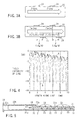
- FIGS. 1 and 2 show the structure of a dielectric leaky-wave antenna 20 according to an embodiment of the present invention.
- the dielectric leaky-wave antenna 20 has a ground plane 21 formed from a flat metallic plate.
- a first dielectric slab 22 constituting the dielectric layer of this embodiment is fixed to an upper surface 21a of the ground plane 21 such that the lower surface of the first dielectric slab 22 tightly contacts the upper surface 21a.
- the first dielectric slab 22 has an almost rectangular outer shape with one convex end.
- a second dielectric slab 23 which forms a transmission guide for transmitting electromagnetic waves between the second dielectric slab 23 and the ground plane 21 is fixed to the upper surface of the first dielectric slab 22 such that the lower surface of the second dielectric slab 23 tightly contacts the upper surface of the first dielectric slab 22.
- the second dielectric slab 23 has the same outer shape as that of the first dielectric slab 22, and overlaps the first dielectric slab 22 so as to match their outer shapes.
- Electromagnetic waves fed from one end of the second dielectric slab 23 travel toward the other end concentratedly through the second dielectric slab 23 having a high permittivity.
- the electromagnetic waves uniformly propagate in the direction of width of the second dielectric slab 23.
- the rectangular portion of the second dielectric slab 23 except for the curved portion extending to one end forms one wide transmission guide in which small-width transmission guides equal in length for transmitting electromagnetic waves from one end to the other end are successively aligned in the direction of width.
- a plurality of (6 in FIGS. 1 and 2) metallic strips 24 having a predetermined width S are parallel-arranged as perturbations of the embodiment on the upper surface of the rectangular portion (transmission guide) of the second dielectric slab 23 at a predetermined interval d with a length equal to the width of the second dielectric slab 23.
- These metallic strips 24 are formed by patterning. In practice, the thickness of the metallic strip 24 is on the ⁇ m order and small to a negligible degree in comparison with that of the second dielectric slab 23.
- the metallic strips 24 are, however, illustrated to be thick in FIGS. 1 and 2 for easy understanding.
- the metallic strips 24 are parallel-arranged on the dielectric slab at a predetermined interval in this way, space harmonics are generated in electromagnetic waves traveling through the slab, and a given one of the electromagnetic waves leaks from the slab surface.
- ⁇ o is the guide wavelength
- ⁇ is the propagation constant of a dielectric line
- k o is a propagation constant in a free space
- n is an integer.
- the radiation amount is determined by the width S of the metallic strip.
- a dielectric layer in this case, the first dielectric slab 22 having a low permittivity is interposed between the ground plane 21 and the second dielectric slab 23, as described above.
- the RF current flowing through the ground plane 21 can decrease to greatly suppress a decrease in antenna efficiency caused by the conductor loss.
- Metallic strips 25 which form pairs of perturbations with the upper-surface-side metallic strips 24 and have the same length and width S as those of the metallic strips 24 are parallel-arranged on the lower surface of the second dielectric slab 23 at the same interval d as that of the metallic strips 24.
- a reflected wave ⁇ greatly varies the electric field in the dielectric line, as represented by curve B in FIG. 4.
- the reflected waves ⁇ a and ⁇ b attain opposite phases to cancel each other.
- FIG. 4 is a graph showing the change characteristic of the electric field in the dielectric line as a function of the distance in the propagation direction when an air layer 0.1 mm in thickness is used as a dielectric layer instead of the first dielectric slab 22.
- the slab warps and may break or crack in the assembly owing to the warpage.
- the wave-front conversion section 26 is formed by extending the second dielectric slab 23 to one end so as to form a dielectric lens, and converts cylindrical waves having a radiation center at the focal position into plane waves parallel in the direction of width of the second dielectric slab 23.
- a matching section 27 for attaining matching between the wave-front conversion section 26 and the feed 30 (to be described later) is formed at the edge of the distal end of the wave-front conversion section 26.
- the feed 30 is an electromagnetic horn type feed made up of a waveguide 30a and horn 30b, and radiates electromagnetic waves input from the waveguide 30a to the wave-front conversion section 26.
- the feed 30 employs an H-plane sectoral horn or E-plane sectoral horn in which the radiation aperture plane suffices to have a small height.
- An H-plane sectoral horn type feed radiates TM-waves having no magnetic field H component in the radiation direction.
- An E-plane sectoral horn type feed radiates TE-waves having no electric field E component in the radiation direction.
- the wave front (equiphase front) of radiated electromagnetic waves is a cylindrical front as far as the horn 30b is not so long.
- cylindrical waves radiated by the feed 30 are converted into plane waves by the wave-front conversion section 26, and the plane waves are incident in phase on one end of the transmission guide formed by the second dielectric slab 23.
- leaky waves in phase in the direction of width are radiated from the surface of the second dielectric slab 23.
- electromagnetic waves of vertical polarization having components in a plane (vertical plane) defined by an electromagnetic wave propagation direction in the second dielectric slab 23 and a direction perpendicular to the slab are radiated.
- the dielectric leaky-wave antenna 20 of this embodiment can obtain design radiation characteristics, and can easily realize a complicated radiation pattern.
- the first dielectric slab 22 serving as a dielectric layer is fixed to the lower surface of the second dielectric slab 23 so as to tightly contact each other.
- the metallic strips 25 are very thin, the first dielectric slab 22 and second dielectric slab 23 do not completely tightly contact each other, and a small air layer is formed at a position where no metallic strips 25 are arranged.
- an air layer may be formed between the first dielectric slab 22 and the second dielectric slab 23 due to slight warpage of the slabs or the like.
- an air layer (or a vacuum layer, or a gas layer other than an air layer) is used as a dielectric layer in place of the first dielectric slab 22.
- the permittivity must be lower than that of the second dielectric slab 23.
- the second dielectric slab 23 is supported on the ground plane 21 via spacers 31 to form an air layer 32 between the ground plane 21 and the second dielectric slab 23, as shown in FIG. 5.
- the spacers 31 in use are small and low in permittivity so as not to influence radiation of leaky waves.
- the dielectric layer is formed by a gas layer other than an air layer
- the gas is sealed between the ground plane 21 and the second dielectric slab 23.
- the metallic strips 24 having a length equal to the width of the second dielectric slab 23 are arranged as perturbations perpendicularly to the electromagnetic wave propagation direction of the transmission guide.
- each metallic strip 34 is selected to constitute a dipole so as to resonate, an RF current flows in the direction of length.
- electromagnetic waves having an angle of 45° with respect to the electromagnetic wave propagation direction of the transmission guide i.e., electromagnetic waves of 45° inclined linear polarization leak.
- radar waves from an automobile traveling on an opposite lane act as interference waves.
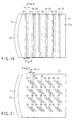
- pairs of metallic strips 34a and 34b laid out to form an angle of 90° may be arranged at the interval d in the electromagnetic wave transmission direction of the transmission guide and a predetermined interval in the direction of width of the transmission guide such that each pair of metallic strips 34a and 34b have an angle of 45° in the electromagnetic wave transmission direction of the transmission guide.
- electromagnetic waves of horizontal polarization or circular polarization can be easily radiated depending on an interval P between a pair of metallic strips 34a and 34b.
- pairs of metallic strips 34a and 34b are arranged on the upper surface of the second dielectric slab 23
- This embodiment uses the metallic strips 24, 25, 34, and 35 as perturbations, but can also use slots instead of these strips.
- slots 37 are formed in metallic frame plates 36 at an angel of 45°, as shown in FIG. 9, in place of the metallic strips 34 and 35, electromagnetic waves of 45° inclined linear polarization can be radiated.
- electromagnetic waves of horizontal linear polarization or circular polarization can be radiated.
- one of a pair of perturbations formed from metallic strips or slots is formed on or in one surface of the second dielectric slab 23, and the other is formed on or in the opposite surface of the second dielectric slab 23.
- a pair of perturbations may be formed on the upper surface of the second dielectric slab 23.
- metallic strips 24 and 25 which have the same length as the width of the dielectric slab 23, are perpendicular to the electromagnetic wave transmission direction of the transmission guide, and are parallel-arranged at an interval ⁇ almost 1/4 the guide wavelength ⁇ g are laid out as pairs of perturbations at a predetermined interval d in the electromagnetic wave transmission direction of the transmission guide.
- slots 37 and 39 (reference numeral 38 denote metallic frame plates) which form an angle of 45° with respect to the electromagnetic wave transmission direction of the transmission guide and are parallel-arranged at an interval almost 1/4 the guide wavelength are laid out as pairs of perturbations at a predetermined interval d in the electromagnetic wave transmission direction of the transmission guide.
- first dielectric slab (dielectric layer) 22 can tightly contact the second dielectric slab 23 to obtain characteristics very close to design ones.
- the length, width, or interval d of each perturbation is set to give desired characteristics to a synthesized wave of an electromagnetic wave leaking from one of the perturbations and an electromagnetic wave leaking from the other.
- the wave-front conversion section 26 is constituted by a dielectric lens formed by extending one end of the second dielectric slab 23.
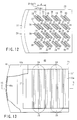
- a parabolic reflector type wave-front conversion section 46 may be adopted, like a dielectric leaky-wave antenna 40 shown in FIGS. 13 to 15 as another embodiment.
- the wave-front conversion section 46 has a reflecting wall 46a for reflecting cylindrical waves and converting them into plane waves, and a guide 46b for guiding the reflected plane waves to one end of a second dielectric slab 23'.
- the wave-front conversion section 46 is attached such that the upper half of the reflecting wall 46a faces one end of the second dielectric slab 23', and the lower half covers the aperture plane of a horn 30b of an electromagnetic horn type feed 30 attached to the lower surface of a ground plane 21.
- Cylindrical waves radiated by the feed 30 are reflected by the reflecting wall 46a of the wave-front conversion section 46, and converted into plane waves, which are input in phase to the transmission guide of the second dielectric slab 23'.
- the feed 30 is arranged on the back surface to reflect electromagnetic waves, so that the entire antenna length can be shortened.
- the dielectric leaky-wave antenna 40 does not require any dielectric lens, so that one end of the second dielectric slab 23' can be linearly shaped (outer shape can be formed into a rectangular).
- a matching section 27 is also linearly formed, which further facilitates processing of the slab.
- a first dielectric slab 22 may be formed from an air layer 32 (or another gas layer) using spacers 31, as shown in FIG. 5.
- the matching section 27 is tapered to decrease the height of the surface side toward the electromagnetic wave input side.
- the matching section 27' is used as a result of analyzing the transmission loss when the height of the aperture portion from the ground plane 21 at the horn 30b of the feed 30 and the guide 46b of the wave-front conversion section 46 is 1.8 mm, the thickness of an alumina second dielectric slab 23 or 23' is 0.64 mm, the tapering length is 8.6 mm, and the thickness of the tapered distal end is 0.2 mm.
- the transmission loss is smaller by almost 0.8 dB within the frequency range of 60 to 90 GHz, and the variation width is much smaller than in the use of the matching section 27.
- the distal end of the dielectric slab must be tapered.
- a matching dielectric having a permittivity different from that of the second dielectric slab 23 or 23' may be attached to the distal end instead of tapering, thereby attaining matching.
- a matching dielectric 41 having a relative permittivity E1 and a width L1 is attached to the distal end of the second dielectric slab 23' to attain matching.
- the matching section 27 or 27' is arranged at one end of the dielectric slab 23 or 23'.
- the matching section can be arranged on the wave-front conversion section 46 or feed 30 side for supplying electromagnetic waves to one end of the dielectric slab 23 or 23'.
- a matching section 46c projecting by a length h toward the ground plane 21 so as to decrease the gap between the matching section 46c and the upper surface of the dielectric slab 23' stepwise toward the dielectric slab is formed continuously in the direction of width at a predetermined depth e inside the aperture of the guide 46b of the wave-front conversion section 46 which is open to surround the edge of one end of the dielectric slab 23'.
- matching section 46c is arranged inside the aperture of the guide 46b, matching between the wave-front conversion section 46 and the transmission guide of the dielectric slab 23' can be attained without tapering the dielectric slab or using a dielectric having a different permittivity, as described above.
- the position of the distal end of the matching section 46c coincides with that of the edge of one end of the dielectric slab 23'.
- the matching section 46c may be arranged to overlap one end of the dielectric slab 23'.
- This matching method can also be used for matching between the horn 30b of the feed 30 and the wave-front conversion section 26 formed by extending one end of the dielectric slab 23.
- a matching section projecting toward the ground plane 21 so as to decrease the gap between the feed 30 and the surface of the wave-front conversion section 26 stepwise is formed continuously in the direction of width at a predetermined depth inside the aperture of the horn 30b which is open to surround the edge of one end of the dielectric slab 23.
- the matching section is also curved in conformity with the edge of the distal end of the wave-front conversion section 26.
- the matching section 46c projects toward the ground plane 21 so as to decrease the gap between the matching section 46c and the upper surface of the dielectric slab 23' stepwise.
- a matching section 46c' may project toward the ground plane 21 so as to decrease the gap between the matching section 46c' and the surface of the dielectric slab 23' stepwise.
- This matching method can also be used for matching between the horn 30b of the feed 30 and the wave-front conversion section 26 formed by extending one end of the dielectric slab 23 as described above.
- the radiation direction (direction of a main beam) is one direction.
- the dielectric leaky-wave antenna 20 or 40 can be used as a multibeam antenna by changing the wave-front conversion section 26 or 46 and the feed 30.
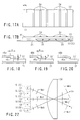
- a dual focus type wave-front conversion section 26' (dielectric lens) is adopted, and a feed 30' is constituted by a plurality of, e.g., five waveguide type radiators 51(1) to 51(5) and a cover 52, like a dielectric leaky-wave antenna 20' shown in FIG. 21.
- Radiation centers C1 to C5 of the radiators are located on or near the focal plane of the wave-front conversion section 26'.
- a cylindrical wave Wa3 radiated by the central radiator 51(3) is converted into a plane wave Wb3 perpendicular to a line L3 (in this case, a straight line parallel to the transmission guide of the second dielectric slab 23) passing from the radiation center C3 through the center of the wave-front conversion section 26'.
- electromagnetic waves are input in phase to the transmission guide of the second dielectric slab 23 to radiate beams along a plane which is perpendicular to the slab surface and includes the propagation direction of the transmission guide.
- This multibeam arrangement can also be applied to the dielectric leaky-wave antenna 40.
- the reflecting wall 46a of the wave-front conversion section 46 is formed into a parabolic shape, and the radiation centers C1 to C5 of a plurality of radiators 51(1) to 51(5) of the feed 30' are located on or near the focal plane.
- the tapered matching section 27 is formed at the distal end of the wave-front conversion section 26' or the distal end of the dielectric slab 23'.
- the matching section 27' or the matching dielectric 41 having a different permittivity may be used in place of the matching section 27.
- a matching section identical to the matching section 46c arranged in the aperture of the guide 46b may be formed to project from the inside of the aperture of the cover 52 toward the ground plane 21.
- electromagnetic waves must be selectively supplied to the radiators 51(1) to 51(5).
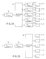
- FIGS. 24 and 25 show examples of a feed circuit.
- an RF circuit 55 converts an IF signal output from the IF circuit 53 into an RF signal, and a switching circuit 56 selectively inputs the RF signal to any one of the radiators 51(1) to 51(5).
- the feed circuit in FIG. 24 for switching an IF signal is more advantageous.
- Either of the circuits to be used is determined in accordance with the intended use.
- each radiator 51 is coupled to the RF circuit 55 or switching circuit 56 via a coupling slot, coupling probe, or the like.
- a dielectric leaky-wave antenna of the present invention which comprises a ground plane, a dielectric slab arranged on one surface of the ground plane to form a transmission guide for transmitting electromagnetic waves along the surface from one end to the other end between the dielectric slab and the ground plane, a perturbation loaded on the dielectric slab to leak the electromagnetic waves from the surface of the dielectric slab, and a feed for supplying the electromagnetic waves to one end of the transmission guide formed by the ground plane and the dielectric slab, a dielectric layer having a lower permittivity than that of the second dielectric slab is interposed between the ground plane and the dielectric slab.
- the current loss of the ground plane can be greatly decreased.
- a milliwave antenna having a very high radiation efficiency with a simple arrangement can be implemented.
- the dielectric layer includes a gas layer including air or a vacuum layer in the dielectric leaky-wave antenna (1). Only the dielectric layer can be interposed between the ground plane and the dielectric slab, and characteristics closer to design values can be obtained.
- the perturbation is formed from a metallic strip or slot perpendicular to the electromagnetic wave transmission direction of the transmission guide in the dielectric leaky-wave antenna (1). Electromagnetic waves of linear polarization can be easily radiated.
- the perturbation is formed from a metallic strip or slot having an angle of 45° with respect to the electromagnetic wave transmission direction of the transmission guide in the dielectric leaky-wave antenna (1). Electromagnetic waves of 45° inclined linear polarization can be easily radiated.
- the perturbation is formed from a pair of metallic strips or pair of slots which form an angle of 90° with each other, and is loaded on the dielectric slab so as to form an angle of 45° with respect to the electromagnetic wave transmission direction of the transmission guide by each metallic strip of the pair of metallic strips or each slot of the pair of slots.
- electromagnetic waves of linear polarization or circular polarization can be easily radiated by selecting the interval between a pair of metallic strips or slots.
- a pair of perturbations parallel-arranged at an interval almost 1/4 the wavelength of the electromagnetic wave in the transmission guide in the electromagnetic wave transmission direction of the transmission guide are loaded at a predetermined interval in the electromagnetic wave transmission direction of the transmission guide in the dielectric leaky-wave antenna (1).
- waves reflected by the perturbation in the transmission guide can be canceled, and disturbance of characteristics by the reflection can be prevented.
- one of the pair of perturbations is formed on one surface of the dielectric slab, and the other is formed on the opposite surface of the dielectric slab in the dielectric leaky-wave antenna (6).
- the pair of perturbations are formed on an upper surface of the dielectric slab in the dielectric leaky-wave antenna (6).
- the dielectric layer can tightly contact the dielectric slab, and characteristics closer to design ones can be obtained.
- the feed is formed to radiate cylindrical waves, and a wave-front conversion section for converting the cylindrical waves radiated by the feed into plane waves and guiding the plane waves to the transmission guide is arranged at one end of the dielectric slab.
- electromagnetic waves in phase can be supplied to the transmission guide formed by the dielectric slab.
- the wave-front conversion section is formed by extending the dielectric slab toward the feed in the dielectric leaky-wave antenna (9).
- the arrangement is simple, wave-front-converted electromagnetic waves can be directly guided to the transmission guide, and the efficiency is high.
- a matching section for matching the feed and the wave-front conversion section and guiding the electromagnetic waves supplied by the feed to the wave-front conversion section is arranged at the distal end of the wave-front conversion section in the dielectric leaky-wave antenna (1). Electromagnetic waves from the feed can be efficiently guided to the wave-front conversion section.
- the feed is formed to transmit electromagnetic waves input from one end to one end of the dielectric slab along the ground plane and to radiate the electromagnetic waves from an aperture at the other end that is formed to surround an edge of the one end of the dielectric slab, and a matching section projecting toward the ground plane so as to decrease a gap between the feed and a surface of the wave-front conversion section stepwise or continuously toward the wave-front conversion section in order to match the feed and the wave-front conversion section is arranged in the aperture at the other end of the feed.
- the feed and wave-front conversion section can be easily matched without tapering the dielectric or using a dielectric having a different permittivity.
- the wave-front conversion section has a reflecting wall for converting cylindrical waves into plane waves and reflecting the plane waves, and is arranged to make one half of the reflecting wall face one end of the dielectric slab, and the feed is arranged on a side opposite to the dielectric slab via the ground plane while the radiation surface faces the other half of the reflecting wall of the wave-front conversion section so as to radiate electromagnetic waves toward the other half.
- the entire antenna length can be shortened.
- a matching section for matching the wave-front conversion section and the transmission guide of the dielectric slab is arranged at one end of the dielectric slab in the dielectric leaky-wave antenna (13). Electromagnetic waves can be efficiently guided from the wave-front conversion section to the dielectric slab.
- the matching section is tapered to decrease the thickness toward the electromagnetic wave input side in the dielectric leaky-wave antenna (11). Electromagnetic waves can be efficiently guided with a simple arrangement.
- the matching section is tapered to decrease the thickness toward the electromagnetic wave input side in the dielectric leaky-wave antenna (14). Electromagnetic waves can be efficiently guided with a simple arrangement.
- the matching section is formed from a dielectric having a permittivity different from that of the dielectric slab in the dielectric leaky-wave antenna (11).
- the dielectric slab can be prevented from breaking and cracking.
- the matching section is formed from a dielectric having a permittivity different from that of the dielectric slab in the dielectric leaky-wave antenna (14).
- the dielectric slab can be prevented from breaking and cracking.
- the wave-front conversion section is formed to transmit electromagnetic waves reflected by the reflecting wall to one end of the dielectric slab along the ground plane and to radiate the electromagnetic waves from an aperture at the other end that is formed to surround the edge of the one end of the dielectric slab, and a matching section projecting toward the ground plane so as to decrease the gap between the feed and the surface of the dielectric slab stepwise or continuously toward the dielectric slab in order to match the wave-front conversion section and the transmission guide of the dielectric slab is arranged in the aperture at the other end of the wave-front conversion section.
- the wave-front conversion section and the transmission guide of the dielectric slab can be easily matched without tapering the dielectric or using a dielectric having a different permittivity.
- the feed has a plurality of radiators having different radiation center positions, and the wave-front conversion section converts cylindrical waves radiated by each radiator into plane waves whose wave front is inclined at an angle corresponding to the radiation center position of the each radiator, and supplies the plane waves to the transmission guide.
- the present invention can provide a dielectric leaky-wave antenna for leaking electromagnetic waves from an electromagnetic wave transmission guide formed by a ground plane and dielectric, in which the structure is simplified and a technique of increasing the antenna efficiency is adopted to meet the conventional demand.
Landscapes
- Waveguide Aerials (AREA)
- Variable-Direction Aerials And Aerial Arrays (AREA)
Applications Claiming Priority (4)
| Application Number | Priority Date | Filing Date | Title |
|---|---|---|---|
| JP2000054487 | 2000-02-29 | ||
| JP2000054487 | 2000-02-29 | ||
| JP2000224271 | 2000-07-25 | ||
| JP2000224271A JP3865573B2 (ja) | 2000-02-29 | 2000-07-25 | 誘電体漏れ波アンテナ |
Publications (2)
| Publication Number | Publication Date |
|---|---|
| EP1130680A2 true EP1130680A2 (fr) | 2001-09-05 |
| EP1130680A3 EP1130680A3 (fr) | 2002-08-07 |
Family
ID=26586434
Family Applications (1)
| Application Number | Title | Priority Date | Filing Date |
|---|---|---|---|
| EP00127989A Ceased EP1130680A3 (fr) | 2000-02-29 | 2000-12-20 | Antenne rayonnante diélectrique à fuites |
Country Status (3)
| Country | Link |
|---|---|
| US (1) | US6489930B2 (fr) |
| EP (1) | EP1130680A3 (fr) |
| JP (1) | JP3865573B2 (fr) |
Cited By (5)
| Publication number | Priority date | Publication date | Assignee | Title |
|---|---|---|---|---|
| EP1313167A1 (fr) * | 2001-11-20 | 2003-05-21 | Smiths Group plc | Antenne avec plaque diélectrique |
| WO2005020372A1 (fr) * | 2003-08-19 | 2005-03-03 | Era Patents Limited | Dispositif de regulation de rayonnement comprenant des elements reactifs sur une surface dielectrique |
| CN101499560A (zh) * | 2008-02-01 | 2009-08-05 | 松下电器产业株式会社 | 端射天线装置 |
| CN102868026A (zh) * | 2011-07-06 | 2013-01-09 | 古野电气株式会社 | 天线装置、雷达装置及电介质部件的配置方法 |
| EP2308128A4 (fr) * | 2008-07-07 | 2013-01-23 | Sierra Nevada Corp | Guide d onde diélectrique plan avec grille métallique pour applications d antenne |
Families Citing this family (21)
| Publication number | Priority date | Publication date | Assignee | Title |
|---|---|---|---|---|
| US6839030B2 (en) * | 2003-05-15 | 2005-01-04 | Anritsu Company | Leaky wave microstrip antenna with a prescribable pattern |
| US7002517B2 (en) * | 2003-06-20 | 2006-02-21 | Anritsu Company | Fixed-frequency beam-steerable leaky-wave microstrip antenna |
| JP4234617B2 (ja) * | 2004-01-30 | 2009-03-04 | 富士通コンポーネント株式会社 | アンテナ装置 |
| US7683464B2 (en) * | 2005-09-13 | 2010-03-23 | Alpha And Omega Semiconductor Incorporated | Semiconductor package having dimpled plate interconnections |
| US7859906B1 (en) | 2007-03-30 | 2010-12-28 | Cypress Semiconductor Corporation | Circuit and method to increase read margin in non-volatile memories using a differential sensing circuit |
| WO2009055895A1 (fr) * | 2007-11-02 | 2009-05-07 | Corporation De L'ecole Polytechnique De Montreal | Antenne dielectrique compacte en couches |
| US8447250B2 (en) * | 2009-06-09 | 2013-05-21 | Broadcom Corporation | Method and system for an integrated voltage controlled oscillator-based transmitter and on-chip power distribution network |
| TWI432124B (zh) * | 2009-11-13 | 2014-03-21 | Advanced Int Multitech Co Ltd | A method of forming a notebook computer case and a product thereof |
| JP5486382B2 (ja) * | 2010-04-09 | 2014-05-07 | 古野電気株式会社 | 2次元スロットアレイアンテナ、給電用導波管、及びレーダ装置 |
| JP5253468B2 (ja) * | 2010-09-03 | 2013-07-31 | 株式会社東芝 | アンテナ装置及びレーダ装置 |
| US9246230B2 (en) * | 2011-02-11 | 2016-01-26 | AMI Research & Development, LLC | High performance low profile antennas |
| EP2717385B1 (fr) * | 2011-06-02 | 2020-05-06 | Panasonic Corporation | Dispositif d'antenne |
| JP6165649B2 (ja) * | 2014-02-04 | 2017-07-19 | 株式会社東芝 | アンテナ装置およびレーダ装置 |
| WO2015120626A1 (fr) * | 2014-02-17 | 2015-08-20 | 华为技术有限公司 | Antenne à calibre commun multibande |
| US11038263B2 (en) * | 2015-11-12 | 2021-06-15 | Duke University | Printed cavities for computational microwave imaging and methods of use |
| US20170294716A1 (en) * | 2016-04-06 | 2017-10-12 | COMSATS Institute of Information Technology, Attock | Tapered microstrip leaky wave antenna |
| US11424548B2 (en) * | 2018-05-01 | 2022-08-23 | Metawave Corporation | Method and apparatus for a meta-structure antenna array |
| WO2019220511A1 (fr) * | 2018-05-14 | 2019-11-21 | 三菱電機株式会社 | Dispositif d'antenne à réseau |
| CN110429375A (zh) * | 2019-07-05 | 2019-11-08 | 惠州市德赛西威智能交通技术研究院有限公司 | 一种宽带基片集成波导双缝天线 |
| CN121605550A (zh) | 2022-11-25 | 2026-03-03 | 京东方科技集团股份有限公司 | 漏波天线、天线阵列及电子设备 |
| CN119093018B (zh) * | 2024-10-08 | 2025-10-21 | 西安电子科技大学 | 高低频分时工作的共形人工表面等离激元相控阵天线 |
Citations (2)
| Publication number | Priority date | Publication date | Assignee | Title |
|---|---|---|---|---|
| US5231411A (en) * | 1991-05-31 | 1993-07-27 | Hughes Aircraft Company | One piece millimeter wave phase shifter/antenna |
| EP0618642A1 (fr) * | 1993-03-31 | 1994-10-05 | Yagi Antenna Co., Ltd. | Radiateur d'ondes électromagnétiques avec un guide d'ondes rayonnant de type NRD |
Family Cites Families (14)
| Publication number | Priority date | Publication date | Assignee | Title |
|---|---|---|---|---|
| US3721988A (en) * | 1971-08-16 | 1973-03-20 | Singer Co | Leaky wave guide planar array antenna |
| US3860934A (en) * | 1973-08-02 | 1975-01-14 | United Aircraft Corp | Unambiguous phase interferometer antenna |
| US4468673A (en) * | 1982-08-18 | 1984-08-28 | The United States Of America As Represented By The Secretary Of The Army | Frequency scan antenna utilizing supported dielectric waveguide |
| US4618865A (en) | 1984-09-27 | 1986-10-21 | Sperry Corporation | Dielectric trough waveguide antenna |
| US4677404A (en) | 1984-12-19 | 1987-06-30 | Martin Marietta Corporation | Compound dielectric multi-conductor transmission line |
| JPS61163704A (ja) | 1985-01-16 | 1986-07-24 | Junkosha Co Ltd | 誘電体線路 |
| JPH0246006A (ja) | 1988-08-08 | 1990-02-15 | Arimura Giken Kk | 分割給電型方形導波線路 |
| JPH02302104A (ja) | 1989-05-16 | 1990-12-14 | Arimura Giken Kk | 方形導波管スロットアレイアンテナ |
| EP0527178A4 (en) | 1990-04-30 | 1993-11-24 | Commonwealth Scientific & Industrial Research Organisation ( C.S.I.R.O. ) | A flat plate antenna |
| US5266961A (en) | 1991-08-29 | 1993-11-30 | Hughes Aircraft Company | Continuous transverse stub element devices and methods of making same |
| US5448252A (en) * | 1994-03-15 | 1995-09-05 | The United States Of America As Represented By The Secretary Of The Air Force | Wide bandwidth microstrip patch antenna |
| JP3269448B2 (ja) | 1997-07-11 | 2002-03-25 | 株式会社村田製作所 | 誘電体線路 |
| US6166693A (en) * | 1998-03-30 | 2000-12-26 | The United States Of America As Represented By The Secretary Of The Army | Tapered leaky wave ultrawide band microstrip antenna |
| US6317095B1 (en) * | 1998-09-30 | 2001-11-13 | Anritsu Corporation | Planar antenna and method for manufacturing the same |
-
2000
- 2000-07-25 JP JP2000224271A patent/JP3865573B2/ja not_active Expired - Fee Related
- 2000-12-19 US US09/741,276 patent/US6489930B2/en not_active Expired - Fee Related
- 2000-12-20 EP EP00127989A patent/EP1130680A3/fr not_active Ceased
Patent Citations (2)
| Publication number | Priority date | Publication date | Assignee | Title |
|---|---|---|---|---|
| US5231411A (en) * | 1991-05-31 | 1993-07-27 | Hughes Aircraft Company | One piece millimeter wave phase shifter/antenna |
| EP0618642A1 (fr) * | 1993-03-31 | 1994-10-05 | Yagi Antenna Co., Ltd. | Radiateur d'ondes électromagnétiques avec un guide d'ondes rayonnant de type NRD |
Cited By (11)
| Publication number | Priority date | Publication date | Assignee | Title |
|---|---|---|---|---|
| EP1313167A1 (fr) * | 2001-11-20 | 2003-05-21 | Smiths Group plc | Antenne avec plaque diélectrique |
| US6819296B2 (en) | 2001-11-20 | 2004-11-16 | Smiths Group Plc | Antennas |
| GB2382468B (en) * | 2001-11-20 | 2005-04-27 | Smiths Group Plc | Antennas |
| WO2005020372A1 (fr) * | 2003-08-19 | 2005-03-03 | Era Patents Limited | Dispositif de regulation de rayonnement comprenant des elements reactifs sur une surface dielectrique |
| EP2077603A3 (fr) * | 2003-08-19 | 2009-07-22 | ERA Technology Limited | Antenne rayonnante diélectrique à fuites |
| CN101499560A (zh) * | 2008-02-01 | 2009-08-05 | 松下电器产业株式会社 | 端射天线装置 |
| CN101499560B (zh) * | 2008-02-01 | 2013-10-30 | 松下电器产业株式会社 | 端射天线装置 |
| EP2308128A4 (fr) * | 2008-07-07 | 2013-01-23 | Sierra Nevada Corp | Guide d onde diélectrique plan avec grille métallique pour applications d antenne |
| US9577342B2 (en) | 2008-07-07 | 2017-02-21 | Sierra Nevada Corporation | Planar dielectric waveguide with metal grid for antenna applications |
| CN102868026A (zh) * | 2011-07-06 | 2013-01-09 | 古野电气株式会社 | 天线装置、雷达装置及电介质部件的配置方法 |
| CN102868026B (zh) * | 2011-07-06 | 2016-08-17 | 古野电气株式会社 | 天线装置、雷达装置及电介质部件的配置方法 |
Also Published As
| Publication number | Publication date |
|---|---|
| US20010017603A1 (en) | 2001-08-30 |
| US6489930B2 (en) | 2002-12-03 |
| EP1130680A3 (fr) | 2002-08-07 |
| JP2001320229A (ja) | 2001-11-16 |
| JP3865573B2 (ja) | 2007-01-10 |
Similar Documents
| Publication | Publication Date | Title |
|---|---|---|
| US6489930B2 (en) | Dielectric leaky-wave antenna | |
| US6597323B2 (en) | Dielectric leaky wave antenna having mono-layer structure | |
| Gandini et al. | SIW slotted waveguide array with pillbox transition for mechanical beam scanning | |
| US6317095B1 (en) | Planar antenna and method for manufacturing the same | |
| JP2648421B2 (ja) | 連続横断スタブ素子を有するアンテナ構造体およびその製造方法 | |
| US10985470B2 (en) | Curved near-field-focused slot array antennas | |
| CN101009401A (zh) | 圆形波导管天线及圆形波导管阵列天线 | |
| EP3888185A1 (fr) | Antenne à onde de fuite à rayonnement transversal alimentée par les deux extrémités | |
| CN112271444A (zh) | 一种高增益双极化siw-cts天线阵 | |
| Sbarra et al. | A novel Rotman lens in SIW technology | |
| WO2015040500A2 (fr) | Système d'alimentation pour groupements d'antennes circulaires à faisceau pouvant être dirigé | |
| Kakhki et al. | Dual complementary source magneto-electric dipole antenna loaded with split ring resonators | |
| US5177496A (en) | Flat slot array antenna for te mode wave | |
| KR102274497B1 (ko) | 파라볼릭-하이퍼볼릭 반사기를 포함하는 안테나 장치 | |
| Roy et al. | Meander Leaky Wave Antenna With Open Stop-Band Suppression for Millimetre Wave Direction-Finding | |
| Sakakibara et al. | High-gain millimeter-wave planar array antennas with traveling-wave excitation | |
| JPH09502587A (ja) | 連続横断スタブ素子装置およびその製造方法 | |
| CN113922061A (zh) | 一种共口径同极化双频波导缝隙天线 | |
| WO1996010277A9 (fr) | Antenne hyperfrequences plane a gain eleve | |
| WO1996010277A1 (fr) | Antenne hyperfrequences plane a gain eleve | |
| Kimura et al. | 76GHz alternating-phase fed single-layer slotted waveguide arrays with suppressed sidelobes in the E-plane | |
| Parellada-Serrano et al. | A fully metallic 3-D mmWave reflectarray with independent polarization steering control | |
| Kimura et al. | An alternating-phase fed single-layer slotted waveguide array in 76 GHz band and its sidelobe suppression | |
| Teshirogi et al. | Dielectric slab based leaky-wave antennas for millimeter-wave applications | |
| Sehm et al. | A 38 GHz horn antenna array |
Legal Events
| Date | Code | Title | Description |
|---|---|---|---|
| PUAI | Public reference made under article 153(3) epc to a published international application that has entered the european phase |
Free format text: ORIGINAL CODE: 0009012 |
|
| 17P | Request for examination filed |
Effective date: 20001220 |
|
| AK | Designated contracting states |
Kind code of ref document: A2 Designated state(s): AT BE CH CY DE DK ES FI FR GB GR IE IT LI LU MC NL PT SE TR |
|
| AX | Request for extension of the european patent |
Free format text: AL;LT;LV;MK;RO;SI |
|
| PUAL | Search report despatched |
Free format text: ORIGINAL CODE: 0009013 |
|
| AK | Designated contracting states |
Kind code of ref document: A3 Designated state(s): AT BE CH CY DE DK ES FI FR GB GR IE IT LI LU MC NL PT SE TR |
|
| AX | Request for extension of the european patent |
Free format text: AL;LT;LV;MK;RO;SI |
|
| AKX | Designation fees paid |
Designated state(s): DE FR GB IT |
|
| 17Q | First examination report despatched |
Effective date: 20030523 |
|
| STAA | Information on the status of an ep patent application or granted ep patent |
Free format text: STATUS: THE APPLICATION HAS BEEN REFUSED |
|
| 18R | Application refused |
Effective date: 20090203 |