EP1131618B1 - Systeme de mesure et methode pour lecture parallele de detecteurs a resonance plasmonique de surface (spr) - Google Patents
Systeme de mesure et methode pour lecture parallele de detecteurs a resonance plasmonique de surface (spr) Download PDFInfo
- Publication number
- EP1131618B1 EP1131618B1 EP99958102A EP99958102A EP1131618B1 EP 1131618 B1 EP1131618 B1 EP 1131618B1 EP 99958102 A EP99958102 A EP 99958102A EP 99958102 A EP99958102 A EP 99958102A EP 1131618 B1 EP1131618 B1 EP 1131618B1
- Authority
- EP
- European Patent Office
- Prior art keywords
- light
- wavelength
- waveguides
- waveguide array
- waveguide
- Prior art date
- Legal status (The legal status is an assumption and is not a legal conclusion. Google has not performed a legal analysis and makes no representation as to the accuracy of the status listed.)
- Expired - Lifetime
Links
Images


Classifications
-
- G—PHYSICS
- G01—MEASURING; TESTING
- G01N—INVESTIGATING OR ANALYSING MATERIALS BY DETERMINING THEIR CHEMICAL OR PHYSICAL PROPERTIES
- G01N21/00—Investigating or analysing materials by the use of optical means, i.e. using sub-millimetre waves, infrared, visible or ultraviolet light
- G01N21/17—Systems in which incident light is modified in accordance with the properties of the material investigated
- G01N21/25—Colour; Spectral properties, i.e. comparison of effect of material on the light at two or more different wavelengths or wavelength bands
- G01N21/251—Colorimeters; Construction thereof
- G01N21/253—Colorimeters; Construction thereof for batch operation, i.e. multisample apparatus
-
- G—PHYSICS
- G01—MEASURING; TESTING
- G01N—INVESTIGATING OR ANALYSING MATERIALS BY DETERMINING THEIR CHEMICAL OR PHYSICAL PROPERTIES
- G01N21/00—Investigating or analysing materials by the use of optical means, i.e. using sub-millimetre waves, infrared, visible or ultraviolet light
- G01N21/17—Systems in which incident light is modified in accordance with the properties of the material investigated
- G01N21/55—Specular reflectivity
- G01N21/552—Attenuated total reflection
- G01N21/553—Attenuated total reflection and using surface plasmons
Definitions
- the invention relates to a measuring arrangement for the parallel reading of SPR sensors (SPR: surface plasmon resonance).
- the light energy is then converted into charge density waves of the electron gas in the gold layer. These charge density waves are called plasmons.
- plasmons charge density waves
- the receptor or ligand is immobilized on the gold surface. Upon addition of the ligand or receptor, the resonance condition is altered upon attachment of the molecules.
- the simplest arrangement for measuring this effect is a glass prism which is illuminated with a light beam and whose angle of incidence is varied (see, for example, "Biospecific interaction analysis using biosensor technology” Malmqvist, M., Nature 361 (1993) 186-187).
- An improved method is the parallel detection of multiple angles.
- the gold surface is illuminated with a slightly divergent monochromatic beam ( ⁇ 10 ° opening angle) and the reflected light is directed onto a spatially resolving light detector. This creates a clear correlation between the angle of reflection and the position on the detector.
- This construction has the advantage of capturing the angular range of interest without moving components. Therefore, this type of detection will be used in some commercial devices, e.g.
- SPM SPR microscopy
- Optical fibers are also used in WO 98/32002 A1.
- the fiber cable is in one Pipette.
- To realize an array is the. Stringing such Pipettes suggested.
- miniaturization is difficult too realize, especially in the parallel measurement of many different Rehearse.
- DE 196 15 366 A1 discloses a method and a device for simultaneous detection of physical, biological or biochemical Reactions and interactions at or in the surface of samples known. All samples are illuminated simultaneously with light of one wavelength irradiated, and the reflected light is transmitted to a receiver array, e.g. one CCD matrix or a video camera supplied. The samples can matrix-like with the sensor surfaces in a plane on a substrate plate be arranged, in turn, on a transparent support plate which is illuminated. The electrical signals of the Receiver arrays are fed to an evaluation device. After Evaluation of samples with one wavelength, this can be another Value to be set.
- a receiver array e.g. one CCD matrix or a video camera supplied.
- the samples can matrix-like with the sensor surfaces in a plane on a substrate plate be arranged, in turn, on a transparent support plate which is illuminated.
- the electrical signals of the Receiver arrays are fed to an evaluation device. After Evaluation of samples with one wavelength, this can be another Value to be set.
- an SPR measuring element which is planar Waveguide is formed.
- an SPR sensor surface provided on which guided in the waveguide light is reflected.
- the bands each correspond to a small angle of incidence range.
- the invention has for its object to provide a measuring arrangement for simultaneous readout of a plurality of SPR sensors, in particular more as a hundred or a thousand, indicate when the readout process should be completed within a measurement time of less than thirty minutes.
- the array used comprises a Variety of waveguides, taking the term waveguide in the frame the invention is an optical medium to understand in which the light in at least one dimension is guided and the at least two parallel Has interfaces.
- a planar SPR sensor 1 is used, which can be produced by means of known silicon semiconductor technologies and arranged to form a waveguide array.
- Fig. 1 a part of such a waveguide array is shown.
- a silicon wafer 11 is provided with an SiO 2 layer 12 serving as an optical buffer against the waveguiding layer 13 and the silicon base material 11.
- the waveguide consists of a silicon oxynitride (SiON) layer 13 having a thickness down to about 10 ⁇ m.
- the Siliziumoxynitrid layer 13 is structured by a dry etching process so that parallel strips 14 with widths between 10 .mu.m to 2000 .mu.m and distances between 10 .mu.m and 5000 .mu.m arise.
- the entire wafer is protected by a cover, not shown, except for the areas which are to carry the SPR-capable metal layer 16 in a later process.
- the unprotected in the previous process step vacancies of the waveguide with a metal layer, which is adapted in thickness to the requirements of the SPR measurement, coated.
- the remaining cover of the wafer is removed.
- these recesses can be generated before or after the application of said metal layer.
- the described technology allows multiple parallel arrays of waveguide structures to be accommodated on a wafer. By etching silicon or by sawing the silicon wafer, the multiple parallel arrangements of waveguide structures are singulated.
- the spatial separation of the individual waveguides with one another at the end at which the SPR sensor is located can be realized by wet-chemical etching of the silicon or a sawing process.
- Another variant of the production of waveguides is the ability to produce polymers in thin layers, for example by spin coating onto a substrate.
- the present in dissolved or uncured form of polymers eg PMMA, polycarbonate, UV-curing adhesives or silicon-containing polymers (Cyclotene or ORMOCERE)
- the refractive index of the carrier material must be smaller than that of the polymer to be applied, which later represents the waveguide.
- the SPR waveguide array is brought into contact with the microtiter plate 60 carrying the samples 61 to be characterized for measurements or coating of the SPR-enabled layers 16.
- the SPR waveguide array is introduced into the microtiter plate 60 until the SPR-capable metal regions are completely wetted by the samples 61.
- the individual, vertically arranged waveguides can be arranged in the horizontal at a distance of any microtiter format.
- a waveguide array of the type described is used in a possible first arrangement described below with reference to FIG. 3.
- an IR filter 4 used in the example to protect the optical components and a monochromator 5 only light of a bandwidth of about 0.5 to 5 nm is transmitted.
- the wavelength selection may also be performed with a filter wheel, requiring a corresponding number of filters of similar bandwidth.
- a beam widening optics (L2, L3) then provides a parallel illumination of the entire waveguide array, in the example via a deflection mirror.
- a multi-hole mask 8 provided in the example according to FIG. 3, which can be designed in a variety of ways, shadows the areas behind which there is no waveguide in order to avoid in advance scattered light which could reach any further undesired paths to a detector which is still provided. Is another, more technically complicated way of ordered parallel attachment and fixing a variety of waveguides, eg.
- a nontransparent material or a material provided with a nontransparent coating can be used for the carrier material used, as a result of which the abovementioned multiple-hole mask 8 can be dispensed with.
- the waveguides themselves, with their sensitive area are in a liquid that can be exchanged to make reference measurements in different solutions, to exchange the target molecules, or to do washes.
- the light emerges in the same angle as it was radiated from the other side (see FIG. 6). In the context of the invention is the.
- Light exit-side waveguide sections further associated with a means 9 which causes a scattering of light emerging from the waveguides light.
- a means 9 which causes a scattering of light emerging from the waveguides light.
- This can, for example, by a separately attachable lens, a suitable coating o.ä. be realized.
- the scattering means 9 the light is scattered diffused.
- This strongly divergent light is imaged directly on a CCD chip 20 with the objective L4.
- the objective L4 is designed so that it covers the entire waveguide array, but only a small part of the light emitted from a light guide light can be detected.
- a cooled high-sensitivity CCD camera 20 is used in the example.
- the required exposure time can be up to a few seconds.
- the light emerging from a single waveguide is imaged simultaneously on a plurality of CCD pixels, which leads to an increase in the detection accuracy.
- the image is provided on several camera pixels, because a CCD chip has a much larger number of pixels than the waveguide array provided here on individual waveguides.
- an image processing software is used, which provides an allocation of the range of several CCD pixels to a single waveguide. This is indicated schematically in FIG. 2, for example the pixel region ⁇ (11, 12), (11, 13), ..., (14, 13) ⁇ is assigned to the waveguide 2, 2, ie the region of the CCD chip 20, on which the image of the waveguide 2,2 is made, comprises 12 pixels.
- This assignment is stored in a computer 30 and is maintained throughout the following measurement, because the array is not moved further in the further.
- a fast program algorithm sums over these camera pixel areas, each associated with a waveguide, so that a single intensity value is obtained and stored for each waveguide. Thereafter, the wavelength of the light irradiated from below in the example is shifted by approximately 1 nm with the aid of the monochromator 5 controlled by the computer 30, and the next intensity value is obtained for all the waveguides. This gives a specific intensity spectrum for each waveguide.
- the exposure of the CCD camera is immediately restarted after the data have arrived at the last wavelength in the computer memory and via the control line 31, a new wavelength is set to a controllable by a stepper motor monochromator ,
- the computer summation over the pixel areas can then be made during the exposure time for the new wavelength. If the exposure time is sufficiently long, the calculation time for the summation is negligible. For each wavelength, the time required is essentially given by the exposure time, which in the example is about 5 seconds. For a spectrum of 200 nm, 16 minutes are required.
- a stronger light source 3 such as a Xe arc lamp
- the light first passes through an IR filter 4, a monochromator 5 and a polarizer 6.
- a beam widening optical system L2, L3 then provides parallel illumination of the waveguide array 10, which in this embodiment, however, is spherical. or gradient lenses L5 are upstream.
- several repositioning of the waveguide array 10 with respect to the lenses L5 provided are necessary.
- the parallel light is then focused by the lenses L5 into the gold coated waveguides, for example, such that in the sensitive region of the waveguide the divergent rays strike the intended metal coating of the waveguide at other angles, even at the angle that enables detection of the SPR.
- the lenses L5 provided in the example, approximately one hundred times the light intensity is coupled into the waveguide with respect to the illumination described in FIG.
- the entrance windows 17 of the waveguides are positioned in the example of the focus of the lenses, ie at a distance of a few 100 microns. It is again important to ensure that no light passes the waveguide, such as through any gaps or transparent areas, in the space of the light exit from the waveguides.
- the means described above for example a multiple-hole mask 8.
- the time required can then be reduced to about 1 second due to the stronger light intensity. For example, if you restrict yourself to a spectrum of sixty wavelengths, one minute is needed for all spectra measured in parallel in the example. This makes it possible, for example, to carry out simultaneous kinetic binding studies with a large number of ligands.
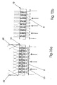
- Figs. 10a and 10b The difference between the illumination of the waveguide array 10 with divergent light of Fig. 4 and the parallel light of Fig. 3 will be demonstrated by Figs. 10a and 10b.
- the marginal rays are shown after passing through the multi-hole mask 8 against the background of a sensor line.
- the marginal rays cover a plurality of measurement areas, so that after emergence the marginal ray can no longer be assigned to a single measurement area. Therefore, when illuminated with divergent light, boundary surfaces 40 must be introduced at least at the edge of the sensor area to ensure total reflection , When illuminated with parallel light ( Figure 10b), these interfaces are not needed. The light beam is guided solely by total reflection at the sensor surface and the opposite interface.
- the light beam penetrates the waveguides from the outset at an angle suitable for SPR resonance. If it is now possible to image the entire parallel emerging light on a CCD detector, also an increase in intensity and thus a shortening of the measurement time can be achieved. Here, however, in contrast to FIG. 3, the angle of the incident light is firmly defined.
- FIG. 3 A more elaborate embodiment, which operates according to this principle with a completely parallel beam path and additionally has improved imaging performance (lower edge shading, lower stray-light sensitivity) is shown in FIG.
- the light is guided through an optical fiber 50 via an optical imaging system L1, L1 'to the monochromator 5 and through a further optical fiber 51 to a beam expansion optics L2, L3.
- the illumination of the waveguide array 10 is carried out as described in FIG. 3 with an expanded parallel beam at an angle below which the plasmon resonance is expected.
- a shadow mask (not shown in FIG. 5) may be used. Upon the exit of the light from the sensor, this occurs either offset in parallel (with an even number of reflections, see Fig. 6b) and thus at the angle ⁇ , under which it has entered. With an odd number of reflections ( Figure 6a), it exits at the angle - ⁇ .
- the length L and width B of the SPR-capable waveguide are specially dimensioned in the example of Figure 5 so that the number of reflections is odd and thus the light exits exclusively in the direction of a second deflection mirror 71.
- the parallelism of the exiting light is exploited here to virtually reverse the light path of the illumination:
- the surface of the sensor array 10 to be imaged is not perpendicular to the optical axis of the arrangement, only one line of the object would be sharply imaged in a conventional camera in which the objective is parallel to the CCD chip due to insufficient depth of focus. Therefore, on the image side, the CCD chip 20 must also be tilted to the optical axis, as indicated in Fig. 5, to ensure over the entire sensor array surface 10 a sharp image.
- the CCD camera is adjusted with a goniometer, not shown, with respect to the lens.
- Another advantage of the telescopic imaging is the low stray light sensitivity, because only light that emerges from the object plane at the detection angle is imaged onto the CCD chip.
- FIG. 7 shows a sharp image of a sensor array 10, produced by a beam guide according to FIG. 5.
- the intensity integral is formed over a sensor area.
- an intensity drop resulting from surface plasmon resonance is detected in the spectrum in this way, as shown by way of example in FIG. 8 for a single example.
- the dashed curve in the upper part of Fig. 8 shows the spectrum in which the sensor surface is in air. Essentially, this corresponds to the mathematical folding of lamp spectrum and monochromator transmission.
- the solid line corresponds to the measurement in the presence. from a buffer; This spectrum is superimposed on the surface plasmon resonance.
- the refractive index of the solution is varied by measuring in different sucrose concentrations.
- the upper part of Figure 9 shows how the dip in the spectrum shifts as expected with increasing sucrose concentration.
- An adaptation of the measured data with a Gaussian function provides numerical values for the position of the minima of the spectra.
- a calibration curve can be obtained therefrom, as can be seen in the lower partial image of FIG. 9. For a sufficiently small region of the refractive index, approximately a linear relationship is assumed here.
Landscapes
- Physics & Mathematics (AREA)
- Health & Medical Sciences (AREA)
- Life Sciences & Earth Sciences (AREA)
- Chemical & Material Sciences (AREA)
- Analytical Chemistry (AREA)
- Biochemistry (AREA)
- General Health & Medical Sciences (AREA)
- General Physics & Mathematics (AREA)
- Immunology (AREA)
- Pathology (AREA)
- Spectroscopy & Molecular Physics (AREA)
- Investigating Or Analysing Materials By Optical Means (AREA)
- Measurement Of Length, Angles, Or The Like Using Electric Or Magnetic Means (AREA)
- Testing Or Calibration Of Command Recording Devices (AREA)
- Arrangements For Transmission Of Measured Signals (AREA)
- Sorting Of Articles (AREA)
Claims (22)
- Dispositif pour effectuer des mesures SPR (SPR: résonance plasmonique de surface), comprenant :une matrice de guides d'onde (10), comprenant une pluralité de guides d'ondes (13) plans, dans lesquels de la lumière est guidée par une face d'entrée de lumière et une face de sortie de lumière, en au moins une dimension, et qui présentent chacun au moins deux faces limites parallèles, les espacements des différents guides d'ondes (13) correspondant à une trame régulière bidimensionnelle et chaque guide d'onde (13) individuel étant muni d'une zone à capteur (16) à capacité SPR,une source d'illumination (3),un groupe (5) à sélectivité de longueur d'onde et un système optique (L2,L3), qui sont disposés en aval de la source d'illumination (3), le système optique (L2,L3) étant réalisé de manière que les faces d'entrée de lumière des guides d'ondes (13) de la matrice de guides d'ondes (10) soient illuminées par de la lumière parallèle, le groupe (5) à sélectivité de longueur d'onde étant réalisé pour régler la longueur d'onde de la lumière à une longueur d'onde de lumière prédéterminée,une optique d'imagerie (L4;L6,L7) et une puce à éléments CCD (20), réalisées de manière que la lumière, sortant des faces de sortie de lumière des guides d'onde (13) de la matrice de guides d'ondes (10) soit imagée sur la puce CCD, et que la lumière sortant de chaque guide d'onde lumineuse (13) individuel soit détectée par chaque fois plusieurs pixels CCD voisins de la puce à éléments CCD (20), et un ordinateur (30) muni d'un logiciel de traitement d'image, réalisés de manière qu'une valeur d'intensité lumineuse, de la lumière sortant de chaque guide d'onde lumineuse (13) individuel, soit calculée et, après avoir procédé à une mémorisation des données concernant la valeur d'intensité, la longueur d'onde réglée et les coordonnées dans la matrice de guides d'onde (10), par l'intermédiaire d'une ligne de commande (31), un réglage du groupe (5) à sélectivité de longueur d'onde à une autre longueur d'onde lumineuse soit effectuée dans le but d'enregistrer un spectre d'intensité.
- Dispositif de mesure selon la revendication 1, caractérisé en ce que, en aval du groupe (5) à sélectivité de longueur d'onde, est installé un polariseur (6).
- Dispositif de mesure selon la revendication 1, caractérisé en ce que les guides d'onde (13) sont réalisés en peigne, de manière que les zones de capteur (16) à capacité SPR puissent être introduites dans les cavités d'une plaque de micro-titrage (60).
- Dispositif de mesure selon la revendication 1 ou 3, caractérisé en ce qu'à la face située côté sortie de la lumière de la matrice de guides d'onde (10) sont associés des moyens de diffusion lumineuse (9).
- Dispositif de mesure selon la revendication 1, 3 ou 4, caractérisé en ce qu'à la face située côté sortie de la lumière de la matrice de guides d'onde (10) sont associés des moyens d'occultation et/ou d'absorption pour assurer qu'arrive à la puce à éléments CCD (20) uniquement de la lumière sortant des guides d'ondes.
- Dispositif de mesure selon la revendication 5, caractérisé en ce qu'à la face située côté entrée de la lumière de la matrice de guides d'onde (10) sont associés des moyens d'occultation se présentant sous la forme d'un masque à pluralité de trous (8).
- Dispositif de mesure selon la revendication 3 ou 5, caractérisé en ce que les moyens d'occultation et/ou d'absorption sont associés de manière que soit effectuée exclusivement une entrée de lumière dans la zone de fond de cavité (62) d'une plaque de micro-titrage (60), dans lesquels sont disposés les capteurs à capacité SPR.
- Dispositif de mesure selon la revendication 3 ou 5, caractérisé en ce que les moyens d'absorption, associés à la face, située côté entrée de la lumière, de la matrice de guides d'onde (10), sont formés sous forme de plaques de micro-titrage, dont les parois latérales de cavités sont fabriquées en un matériau absorbant la lumière.
- Dispositif de mesure selon la revendication 5, caractérisé en ce que les moyens d'absorption, associés à la face, située côté entrée de la lumière, de la matrice de guides d'onde (10), sont réalisés sous forme d'un produit coulé, absorbant la lumière, séparant les uns des autres les guides d'ondes (13).
- Dispositif de mesure selon la revendication 1, caractérisé en ce que le groupe (5) à sélectivité de longueur d'onde est formé par un mono-chromateur réglable pas à pas et, en aval du système d'imagerie optique (L2,L3), est installé un miroir de renvoi (7), assurant une occultation des faces d'entrée de lumière des guides d'ondes (13) par une lumière parallèle, au-dessous d'un angle approprié.
- Dispositif de mesure selon la revendication 10, caractérisé en ce qu'en plus, en aval de l'extrémité située côté sortie de la lumière de la matrice de guides d'onde (10), est directement installé un autre miroir de renvoi (71), assurant l'imagerie de la matrice de guides d'onde (10) sur une puce à éléments CCD (20) inclinée par rapport à l'axe optique.
- Procédé de mesure pour des mesures SPR (SPR: résonance plasmanique de surface), comprenant :l'utilisation d'une matrice de guides d'onde (10), comprenant une pluralité de guides d'ondes plans, dans lesquels de la lumière est guidée par une face d'entrée de lumière et une face de sortie de lumière, en au moins une dimension, et qui présentent chacun au moins deux faces limites parallèles, les espacements entre les différents guides d'ondes (13) correspondant à une trame régulière bidimensionnelle et chaque guide d'onde (13) individuel étant muni d'une zone de capteurs (16) à capacité SPR,l'élimination des faces d'entrée de lumière des guides d'onde (13) de la matrice de guides de lumière (10) par de la lumière parallèle avec une source d'illumination (3), d'un groupe (5) à sélectivité de longueur d'onde et d'un système (L2,L3) optique, le groupe (5) à sélectivité de longueur d'onde réglant la longueur d'onde de la lumière à une longueur d'onde lumineuse prédéterminée,l'imagerie de la lumière sortant des faces de sortie de lumière des guides d'ondes (13) de la matrice de guides d'ondes (11) sur une puce à éléments CCD (20) avec une optique d'imagerie (L4; L6, L7), et détection de la lumière sortant de chaque guide d'onde lumineuse (13) individuel, au moyen de la pluralité des pixels CCD voisins de la puce à éléments CCD 20, etcalcul d'une valeur d'intensité de lumière de la lumière sortant de chaque guide d'ondes de lumière (13) individuel avec un ordinateur (30) muni d'un logiciel de traitement d'image, et, après stockage des données concernant la valeur d'intensité, de la longueur d'onde réglée et des coordonnées dans la matrice de guides d'ondes (10), réglage du groupe (5) à sélectivité de longueur d'onde, pour une autre longueur d'onde lumineuse, dans le but d'enregistrement d'un spectre d'intensité.
- Procédé de mesure selon la revendication 12, caractérisé en ce que, en aval du groupe (5) à sélectivité de longueur d'onde, est installé un polariseur (6).
- Procédé de mesure selon la revendication 12, caractérisé en ce que les guides d'ondes (13) sont réalisés en un genre de peigne, de manière que les zones de capteur à capacité SPR puissent être introduits dans les cavités d'une plaque de micro-titrage (60).
- Procédé de mesure selon la revendication 12 ou 14, caractérisé en ce que la lumière, sur la face, située côté sortie de la lumière, de la matrice de guides d'ondes (10), est diffusée à l'aide de moyens photo-diffuseurs (9).
- Procédé de mesure selon la revendication 12, 14 ou 15, caractérisé en ce que, sur la face, située du côté entrée de lumière, de la matrice de guides d'ondes (10), de la lumière est occultée à l'aide de moyens d'occultation et/ou d'absorption pour assurer qu'arrive à la puce à éléments CCD uniquement de la lumière sortant des guides d'onde.
- Procédé de mesure selon la revendication 16, caractérisé en ce que, à la face, située du côté entrée de la lumière, de la matrice à guide d'onde (10), sont associés des moyens d'occultation réalisés sous la forme d'un masque à trous multiples (8).
- Procédé de mesure selon la revendication 14 ou 16, caractérisé en ce que les moyens d'occultation et/ou d'absorption sont associés de manière que soit effectuée exclusivement une entrée de lumière dans les zones de fond des cavités (62) d'une plaque de micro-titrage (60), dans lesquelles sont disposés les capteurs à capacité SPR.
- Procédé de mesure selon la revendication 14 ou 16, caractérisé en ce que les moyens d'absorption, associés à la face, située côté entrée de la lumière, de la matrice de guides d'onde (10), sont réalisés sous la forme d'une plaque de micro-titrage dont les parois latérales de cavités sont fabriquées à partir d'un matériau absorbant la lumière.
- Procédé de mesure selon la revendication 16, caractérisé en ce que les moyens d'absorption, associés à la face, située du côté entrée de la lumière, de la matrice de guides d'onde (10), sont réalisés sous la forme d'un produit moulé absorbant la lumière, séparant les guides d'onde (13) les uns des autres.
- Procédé de mesure selon la revendication 12, caractérisé en ce que le groupe (5) à sélectivité de longueur d'onde est formé par un monochromateur réglable pas à pas et, en aval du système d'imagerie optique (L2,L3), est installé un miroir de renvoi (7), pour assurer un éclairement des faces d'entrée de lumière des guides d'onde (13) avec de la lumière parallèle, sous un angle approprié.
- Procédé de mesure selon la revendication 20, caractérisé en ce que, en plus de l'extrémité, située côté sortie de la lumière, de la matrice de guides d'onde (17), est installé en aval, directement, un autre miroir de renvoi (71), pour assurer l'imagerie de la matrice de guides d'onde (10), sur une puce à éléments CCD (20) inclinée par rapport à l'axe optique.
Applications Claiming Priority (3)
| Application Number | Priority Date | Filing Date | Title |
|---|---|---|---|
| DE19854370 | 1998-11-20 | ||
| DE19854370 | 1998-11-20 | ||
| PCT/EP1999/008977 WO2000031515A1 (fr) | 1998-11-20 | 1999-11-16 | Systeme de mesure pour selection parallele de detecteurs par resonance plasmonique de surface (spr) |
Publications (2)
| Publication Number | Publication Date |
|---|---|
| EP1131618A1 EP1131618A1 (fr) | 2001-09-12 |
| EP1131618B1 true EP1131618B1 (fr) | 2005-10-12 |
Family
ID=7888969
Family Applications (1)
| Application Number | Title | Priority Date | Filing Date |
|---|---|---|---|
| EP99958102A Expired - Lifetime EP1131618B1 (fr) | 1998-11-20 | 1999-11-16 | Systeme de mesure et methode pour lecture parallele de detecteurs a resonance plasmonique de surface (spr) |
Country Status (10)
| Country | Link |
|---|---|
| US (1) | US6441906B2 (fr) |
| EP (1) | EP1131618B1 (fr) |
| JP (1) | JP2002530668A (fr) |
| AT (1) | ATE306658T1 (fr) |
| AU (1) | AU751246B2 (fr) |
| CA (1) | CA2351454A1 (fr) |
| DE (2) | DE19955556B4 (fr) |
| DK (1) | DK1131618T3 (fr) |
| ES (1) | ES2251244T3 (fr) |
| WO (1) | WO2000031515A1 (fr) |
Families Citing this family (29)
| Publication number | Priority date | Publication date | Assignee | Title |
|---|---|---|---|---|
| US6559939B1 (en) * | 1999-10-29 | 2003-05-06 | Avery Dennison Corporation | Method of high throughput haze screening of material |
| ATE353438T1 (de) | 2000-02-22 | 2007-02-15 | Santhera Pharmaceuticals Deuts | Spr-sensorsystem |
| DE10008006C2 (de) * | 2000-02-22 | 2003-10-16 | Graffinity Pharm Design Gmbh | SPR-Sensor und SPR-Sensoranordnung |
| DE10020313C1 (de) * | 2000-04-20 | 2001-07-05 | Cybio Systems Gmbh | Anordnung zur elektrochemischen Analyse mittels Oberflächenplasmonenresonanz |
| US6747737B2 (en) * | 2000-06-29 | 2004-06-08 | Carl Zeiss Jena Gmbh | Method for optical detection of an illuminated specimen in a plurality of detection channels |
| DE10055655C2 (de) * | 2000-11-10 | 2003-06-12 | Jandratek Gmbh | Plasmonenresonanzsensor, insbesondere für die Biosensorik |
| US7030988B2 (en) | 2001-03-22 | 2006-04-18 | Fuji Photo Film Co., Ltd. | Measuring apparatus and measuring chip |
| US6734956B2 (en) * | 2002-05-06 | 2004-05-11 | Reichert, Inc. | Optical configuration and method for differential refractive index measurements |
| JP4109022B2 (ja) * | 2002-06-13 | 2008-06-25 | 富士フイルム株式会社 | 測定装置および該測定装置の使用方法 |
| US6804007B2 (en) * | 2002-09-10 | 2004-10-12 | Reichert, Inc. | Apparatus for multiplexing two surface plasma resonance channels onto a single linear scanned array |
| JP4173746B2 (ja) * | 2003-02-12 | 2008-10-29 | 富士フイルム株式会社 | 測定装置 |
| US7292333B2 (en) * | 2003-06-24 | 2007-11-06 | Corning Incorporated | Optical interrogation system and method for 2-D sensor arrays |
| US7057720B2 (en) | 2003-06-24 | 2006-06-06 | Corning Incorporated | Optical interrogation system and method for using same |
| WO2005022131A1 (fr) * | 2003-08-27 | 2005-03-10 | Toyo Boseki Kabushiki Kaisha | Dispositif de resonance plasmonique de surface |
| EP1659395A4 (fr) * | 2003-12-26 | 2009-10-21 | Panasonic Corp | Procede d'analyse d'un ligand dans un echantillon et appareil d'analyse d'un ligand dans un echantillon |
| JP3890362B2 (ja) * | 2004-06-17 | 2007-03-07 | 国立大学法人室蘭工業大学 | 表面プラズモン共鳴現象測定装置 |
| US7659987B2 (en) * | 2004-09-16 | 2010-02-09 | Canon Kabushiki Kaisha | Device and method for acquiring information on objective substance to be detected by detecting a change of wavelength characteristics on the optical transmittance |
| US7317519B2 (en) * | 2004-10-29 | 2008-01-08 | Agilent Technologies, Inc. | Swept-angle SPR measurement system |
| CN100520394C (zh) * | 2005-03-08 | 2009-07-29 | 中国科学院电子学研究所 | 一种单通道多参数表面等离子体谐振测试仪 |
| DE102005023489B4 (de) * | 2005-05-17 | 2014-01-30 | Dr. Johannes Heidenhain Gmbh | Positionsmesseinrichtung zur Bestimmung der Position zweier entlang einer Messrichtung zueinander beweglicher Objekte und Verfahren zur Bildung eines Referenzimpulses für eine derartige Positionsmesseinrichtung |
| US7483127B1 (en) * | 2005-08-08 | 2009-01-27 | Sru Biosystems, Inc. | Method and apparatus for generating an image of biomolecular sensor target area |
| EP2041583A1 (fr) * | 2006-06-30 | 2009-04-01 | Corning Incorporated | Système de manipulation de fluides destiné à un dispositif d'analyse à renouvellement continu |
| US8743367B2 (en) * | 2007-05-21 | 2014-06-03 | Bio-Rad Laboratories Inc. | Optical resonance analysis using a multi-angle source of illumination |
| KR100865755B1 (ko) * | 2007-06-29 | 2008-10-28 | 삼성전기주식회사 | 표면 플라즈몬 공명을 이용한 다채널 바이오 센서 |
| US8530243B2 (en) | 2009-04-20 | 2013-09-10 | Bio-Rad Laboratories Inc. | Non-scanning SPR system |
| US10481089B2 (en) * | 2013-03-12 | 2019-11-19 | Integrated Plasmonics Corporation | Optical detection system with tilted sensor |
| JP7205851B2 (ja) * | 2018-05-30 | 2023-01-17 | 国立大学法人東京工業大学 | 屈折率測定装置、屈折率測定方法およびプログラム |
| US11513074B2 (en) * | 2018-07-11 | 2022-11-29 | Ofek—Eshkolot Research And Development Ltd. | Method and device for detecting extracellular vesicles |
| CN112665618B (zh) * | 2020-12-17 | 2022-05-17 | 安徽中元新材料技术有限公司 | 一种基于形态学的波长敏感模式提取装置及方法 |
Citations (2)
| Publication number | Priority date | Publication date | Assignee | Title |
|---|---|---|---|---|
| US5485277A (en) * | 1994-07-26 | 1996-01-16 | Physical Optics Corporation | Surface plasmon resonance sensor and methods for the utilization thereof |
| WO1997015819A1 (fr) * | 1995-10-25 | 1997-05-01 | University Of Washington | Capteur a conducteur de lumiere, a plasmon en surface |
Family Cites Families (16)
| Publication number | Priority date | Publication date | Assignee | Title |
|---|---|---|---|---|
| CA1237645A (fr) * | 1982-12-21 | 1988-06-07 | John H. Fisher | Technique analytique |
| NL8700851A (nl) * | 1987-04-10 | 1988-11-01 | Tno | Werkwijze en inrichting voor het detecteren van zeer lage concentraties van een in een meetmedium aanwezige chemische component onder toepassing van oppervlakte-plasmonresonantie en elektrochemisch gestimuleerde adsorptie. |
| GB8811919D0 (en) * | 1988-05-20 | 1988-06-22 | Amersham Int Plc | Biological sensors |
| SE462408B (sv) * | 1988-11-10 | 1990-06-18 | Pharmacia Ab | Optiskt biosensorsystem utnyttjande ytplasmonresonans foer detektering av en specific biomolekyl, saett att kalibrera sensoranordningen samt saett att korrigera foer baslinjedrift i systemet |
| DE3909144A1 (de) * | 1989-03-21 | 1990-09-27 | Basf Ag | Verfahren zur bestimmung von brechungsindex und schichtdicke duenner schichten |
| US5359681A (en) * | 1993-01-11 | 1994-10-25 | University Of Washington | Fiber optic sensor and methods and apparatus relating thereto |
| DE4315211A1 (de) * | 1993-05-07 | 1994-02-03 | Gunnar Brink | Vorrichtung und Verfahren zum Nachweis der Adsorption von Molekülen mittels Nahinfrarot-Oberflächenplasmonenresonanz |
| FI96800C (fi) * | 1994-02-16 | 1996-08-26 | Valtion Teknillinen | Laite analyysin suorittamiseksi |
| AT403745B (de) * | 1996-02-29 | 1998-05-25 | Avl Verbrennungskraft Messtech | Messanordnung mit einem für anregungs- und messstrahlung transparentem trägerelement |
| EP0797091A1 (fr) * | 1996-03-19 | 1997-09-24 | Texas Instruments Incorporated | Capteur à resonance de plasmon de surface avec element optique remplacable |
| DE19615366B4 (de) * | 1996-04-19 | 2006-02-09 | Carl Zeiss Jena Gmbh | Verfahren und Einrichtung zum Nachweis physikalischer, chemischer, biologischer oder biochemischer Reaktionen und Wechselwirkungen |
| US5917607A (en) * | 1996-04-25 | 1999-06-29 | Fuji Photo Film Co., Ltd. | Surface plasmon sensor for multiple channel analysis |
| WO1998032002A1 (fr) * | 1997-01-22 | 1998-07-23 | Biacore Ab | Pipette et ensemble support pour capteurs |
| DE19748211A1 (de) * | 1997-10-31 | 1999-05-06 | Zeiss Carl Fa | Optisches Array-System und Reader für Mikrotiterplatten |
| DE19814811C1 (de) * | 1998-04-02 | 1999-08-05 | Inst Physikalische Hochtech Ev | Anordnung für die Oberflächenplasmonen-Resonanz-Spektroskopie |
| JP2002518663A (ja) * | 1998-05-20 | 2002-06-25 | グラッフィニティ ファルマシューティカル デザイン ゲーエムベーハー | 液体状態で存在する多数の試料を同時に測定するためのsprセンサー |
-
1999
- 1999-11-16 AT AT99958102T patent/ATE306658T1/de not_active IP Right Cessation
- 1999-11-16 DE DE19955556A patent/DE19955556B4/de not_active Expired - Fee Related
- 1999-11-16 JP JP2000584279A patent/JP2002530668A/ja active Pending
- 1999-11-16 CA CA002351454A patent/CA2351454A1/fr not_active Abandoned
- 1999-11-16 AU AU15559/00A patent/AU751246B2/en not_active Ceased
- 1999-11-16 DE DE59912658T patent/DE59912658D1/de not_active Expired - Lifetime
- 1999-11-16 WO PCT/EP1999/008977 patent/WO2000031515A1/fr not_active Ceased
- 1999-11-16 DK DK99958102T patent/DK1131618T3/da active
- 1999-11-16 ES ES99958102T patent/ES2251244T3/es not_active Expired - Lifetime
- 1999-11-16 EP EP99958102A patent/EP1131618B1/fr not_active Expired - Lifetime
-
2001
- 2001-05-18 US US09/859,677 patent/US6441906B2/en not_active Expired - Fee Related
Patent Citations (2)
| Publication number | Priority date | Publication date | Assignee | Title |
|---|---|---|---|---|
| US5485277A (en) * | 1994-07-26 | 1996-01-16 | Physical Optics Corporation | Surface plasmon resonance sensor and methods for the utilization thereof |
| WO1997015819A1 (fr) * | 1995-10-25 | 1997-05-01 | University Of Washington | Capteur a conducteur de lumiere, a plasmon en surface |
Also Published As
| Publication number | Publication date |
|---|---|
| DE19955556A1 (de) | 2000-06-08 |
| AU1555900A (en) | 2000-06-13 |
| JP2002530668A (ja) | 2002-09-17 |
| US20020001085A1 (en) | 2002-01-03 |
| EP1131618A1 (fr) | 2001-09-12 |
| ATE306658T1 (de) | 2005-10-15 |
| WO2000031515A1 (fr) | 2000-06-02 |
| DK1131618T3 (da) | 2006-02-20 |
| DE59912658D1 (de) | 2005-11-17 |
| CA2351454A1 (fr) | 2000-06-02 |
| AU751246B2 (en) | 2002-08-08 |
| US6441906B2 (en) | 2002-08-27 |
| DE19955556B4 (de) | 2004-09-09 |
| ES2251244T3 (es) | 2006-04-16 |
Similar Documents
| Publication | Publication Date | Title |
|---|---|---|
| EP1131618B1 (fr) | Systeme de mesure et methode pour lecture parallele de detecteurs a resonance plasmonique de surface (spr) | |
| EP1257809B1 (fr) | Detecteur spr et dispositif de detection spr | |
| EP1259796B1 (fr) | Systeme de detection par resonance plasmonique de surface | |
| DE19923820C2 (de) | SPR-Sensor zur gleichzeitigen Erfassung einer Vielzahl von in fluider Form vorliegenden Proben | |
| DE19732619C2 (de) | Optische Detektoreinrichtung | |
| EP1307728B1 (fr) | Structure reticulaire de guide d'ondes et dispositif de mesure optique | |
| EP3428622B1 (fr) | Biocapteur diffractif | |
| DE19615366B4 (de) | Verfahren und Einrichtung zum Nachweis physikalischer, chemischer, biologischer oder biochemischer Reaktionen und Wechselwirkungen | |
| DE69933193T2 (de) | Integrierter optischer Sensor und Verfahren zum integrierten optischen Nachweis einer Substanz | |
| DE69929075T2 (de) | Biochip mit einer mehrzahl von bereichen zur molekularen erkennung, und dazu geeignete auslesevorrichtung | |
| EP1166090B1 (fr) | Dispositif permettant de mesurer rapidement la diffraction angle-dependante sur des surfaces finement structurees | |
| EP0469377B1 (fr) | Dispositif et procédé pour la détermination d'une analyte dans un échantillon liquide | |
| EP0988526A1 (fr) | Dispositif de detection de substances chimiques et biochimiques par excitation de lumiere fluorescente et son procede de production | |
| EP0618441A2 (fr) | Dispositif pour examiner par résolution latérale une couche ultra-mince à hétérogènéité latérale | |
| DE10052165A1 (de) | SPR-Sensorsystem | |
| DE69120253T2 (de) | Apparat zur fluoreszenzanalyse | |
| DE102018133037B4 (de) | Anordnung und Verfahren zur Erfassung von optischen Eigenschaften einer Probe, insbesondere zum selektiven Nachweis von biologischen Molekülen und zum Auslesen einer Molekülbelegung | |
| AT5152U1 (de) | Spr-sensorsystem |
Legal Events
| Date | Code | Title | Description |
|---|---|---|---|
| PUAI | Public reference made under article 153(3) epc to a published international application that has entered the european phase |
Free format text: ORIGINAL CODE: 0009012 |
|
| 17P | Request for examination filed |
Effective date: 20010605 |
|
| AK | Designated contracting states |
Kind code of ref document: A1 Designated state(s): AT BE CH CY DE DK ES FI FR GB GR IE IT LI LU MC NL PT SE |
|
| AX | Request for extension of the european patent |
Free format text: AL;LT;LV;MK;RO;SI |
|
| 17Q | First examination report despatched |
Effective date: 20021129 |
|
| GRAP | Despatch of communication of intention to grant a patent |
Free format text: ORIGINAL CODE: EPIDOSNIGR1 |
|
| RTI1 | Title (correction) |
Free format text: MEASURING APPARATUS AND METHOD FOR PARALLEL READOUT OF SPR SENSORS |
|
| GRAS | Grant fee paid |
Free format text: ORIGINAL CODE: EPIDOSNIGR3 |
|
| GRAA | (expected) grant |
Free format text: ORIGINAL CODE: 0009210 |
|
| AK | Designated contracting states |
Kind code of ref document: B1 Designated state(s): AT BE CH CY DE DK ES FI FR GB GR IE IT LI LU MC NL PT SE |
|
| PG25 | Lapsed in a contracting state [announced via postgrant information from national office to epo] |
Ref country code: IE Free format text: LAPSE BECAUSE OF FAILURE TO SUBMIT A TRANSLATION OF THE DESCRIPTION OR TO PAY THE FEE WITHIN THE PRESCRIBED TIME-LIMIT Effective date: 20051012 Ref country code: FI Free format text: LAPSE BECAUSE OF FAILURE TO SUBMIT A TRANSLATION OF THE DESCRIPTION OR TO PAY THE FEE WITHIN THE PRESCRIBED TIME-LIMIT Effective date: 20051012 |
|
| REG | Reference to a national code |
Ref country code: GB Ref legal event code: FG4D Free format text: NOT ENGLISH |
|
| REG | Reference to a national code |
Ref country code: CH Ref legal event code: EP |
|
| PGFP | Annual fee paid to national office [announced via postgrant information from national office to epo] |
Ref country code: PT Payment date: 20051021 Year of fee payment: 7 |
|
| GBT | Gb: translation of ep patent filed (gb section 77(6)(a)/1977) |
Effective date: 20051012 |
|
| REG | Reference to a national code |
Ref country code: IE Ref legal event code: FG4D Free format text: LANGUAGE OF EP DOCUMENT: GERMAN |
|
| PGFP | Annual fee paid to national office [announced via postgrant information from national office to epo] |
Ref country code: AT Payment date: 20051114 Year of fee payment: 7 |
|
| PG25 | Lapsed in a contracting state [announced via postgrant information from national office to epo] |
Ref country code: IT Free format text: LAPSE BECAUSE OF NON-PAYMENT OF DUE FEES Effective date: 20051116 Ref country code: CY Free format text: LAPSE BECAUSE OF FAILURE TO SUBMIT A TRANSLATION OF THE DESCRIPTION OR TO PAY THE FEE WITHIN THE PRESCRIBED TIME-LIMIT Effective date: 20051116 |
|
| REF | Corresponds to: |
Ref document number: 59912658 Country of ref document: DE Date of ref document: 20051117 Kind code of ref document: P |
|
| PGFP | Annual fee paid to national office [announced via postgrant information from national office to epo] |
Ref country code: DK Payment date: 20051124 Year of fee payment: 7 |
|
| PGFP | Annual fee paid to national office [announced via postgrant information from national office to epo] |
Ref country code: ES Payment date: 20051128 Year of fee payment: 7 Ref country code: BE Payment date: 20051128 Year of fee payment: 7 |
|
| PG25 | Lapsed in a contracting state [announced via postgrant information from national office to epo] |
Ref country code: MC Free format text: LAPSE BECAUSE OF NON-PAYMENT OF DUE FEES Effective date: 20051130 |
|
| PGFP | Annual fee paid to national office [announced via postgrant information from national office to epo] |
Ref country code: NL Payment date: 20051130 Year of fee payment: 7 |
|
| PGFP | Annual fee paid to national office [announced via postgrant information from national office to epo] |
Ref country code: SE Payment date: 20051202 Year of fee payment: 7 |
|
| PG25 | Lapsed in a contracting state [announced via postgrant information from national office to epo] |
Ref country code: LU Free format text: LAPSE BECAUSE OF NON-PAYMENT OF DUE FEES Effective date: 20051212 |
|
| REG | Reference to a national code |
Ref country code: CH Ref legal event code: NV Representative=s name: NOVAGRAAF INTERNATIONAL SA |
|
| REG | Reference to a national code |
Ref country code: SE Ref legal event code: TRGR |
|
| PG25 | Lapsed in a contracting state [announced via postgrant information from national office to epo] |
Ref country code: GR Free format text: LAPSE BECAUSE OF FAILURE TO SUBMIT A TRANSLATION OF THE DESCRIPTION OR TO PAY THE FEE WITHIN THE PRESCRIBED TIME-LIMIT Effective date: 20060112 |
|
| REG | Reference to a national code |
Ref country code: DK Ref legal event code: T3 |
|
| REG | Reference to a national code |
Ref country code: ES Ref legal event code: FG2A Ref document number: 2251244 Country of ref document: ES Kind code of ref document: T3 |
|
| REG | Reference to a national code |
Ref country code: IE Ref legal event code: FD4D |
|
| ET | Fr: translation filed | ||
| PLBE | No opposition filed within time limit |
Free format text: ORIGINAL CODE: 0009261 |
|
| STAA | Information on the status of an ep patent application or granted ep patent |
Free format text: STATUS: NO OPPOSITION FILED WITHIN TIME LIMIT |
|
| 26N | No opposition filed |
Effective date: 20060713 |
|
| PG25 | Lapsed in a contracting state [announced via postgrant information from national office to epo] |
Ref country code: AT Free format text: LAPSE BECAUSE OF NON-PAYMENT OF DUE FEES Effective date: 20061116 |
|
| PG25 | Lapsed in a contracting state [announced via postgrant information from national office to epo] |
Ref country code: SE Free format text: LAPSE BECAUSE OF NON-PAYMENT OF DUE FEES Effective date: 20061117 |
|
| PG25 | Lapsed in a contracting state [announced via postgrant information from national office to epo] |
Ref country code: DK Free format text: LAPSE BECAUSE OF NON-PAYMENT OF DUE FEES Effective date: 20061130 Ref country code: BE Free format text: LAPSE BECAUSE OF NON-PAYMENT OF DUE FEES Effective date: 20061130 |
|
| PG25 | Lapsed in a contracting state [announced via postgrant information from national office to epo] |
Ref country code: PT Free format text: LAPSE BECAUSE OF NON-PAYMENT OF DUE FEES Effective date: 20070516 |
|
| REG | Reference to a national code |
Ref country code: PT Ref legal event code: MM4A Free format text: LAPSE DUE TO NON-PAYMENT OF FEES Effective date: 20070516 |
|
| PG25 | Lapsed in a contracting state [announced via postgrant information from national office to epo] |
Ref country code: NL Free format text: LAPSE BECAUSE OF NON-PAYMENT OF DUE FEES Effective date: 20070601 |
|
| REG | Reference to a national code |
Ref country code: DK Ref legal event code: EBP |
|
| EUG | Se: european patent has lapsed | ||
| NLV4 | Nl: lapsed or anulled due to non-payment of the annual fee |
Effective date: 20070601 |
|
| BERE | Be: lapsed |
Owner name: *GRAFFINITY PHARMACEUTICAL DESIGN G.M.B.H. Effective date: 20061130 |
|
| REG | Reference to a national code |
Ref country code: ES Ref legal event code: FD2A Effective date: 20061117 |
|
| PG25 | Lapsed in a contracting state [announced via postgrant information from national office to epo] |
Ref country code: ES Free format text: LAPSE BECAUSE OF NON-PAYMENT OF DUE FEES Effective date: 20061117 |
|
| PGFP | Annual fee paid to national office [announced via postgrant information from national office to epo] |
Ref country code: GB Payment date: 20101020 Year of fee payment: 12 |
|
| REG | Reference to a national code |
Ref country code: CH Ref legal event code: PFA Owner name: GRAFFINITY PHARMACEUTICAL DESIGN GMBH Free format text: GRAFFINITY PHARMACEUTICAL DESIGN GMBH#IM NEUENHEIMER FELD 515#69120 HEIDELBERG (DE) -TRANSFER TO- GRAFFINITY PHARMACEUTICAL DESIGN GMBH#IM NEUENHEIMER FELD 515#69120 HEIDELBERG (DE) |
|
| PGFP | Annual fee paid to national office [announced via postgrant information from national office to epo] |
Ref country code: CH Payment date: 20111031 Year of fee payment: 13 Ref country code: FR Payment date: 20111201 Year of fee payment: 13 |
|
| REG | Reference to a national code |
Ref country code: CH Ref legal event code: PL |
|
| GBPC | Gb: european patent ceased through non-payment of renewal fee |
Effective date: 20121116 |
|
| PG25 | Lapsed in a contracting state [announced via postgrant information from national office to epo] |
Ref country code: CH Free format text: LAPSE BECAUSE OF NON-PAYMENT OF DUE FEES Effective date: 20121130 Ref country code: LI Free format text: LAPSE BECAUSE OF NON-PAYMENT OF DUE FEES Effective date: 20121130 |
|
| REG | Reference to a national code |
Ref country code: FR Ref legal event code: ST Effective date: 20130731 |
|
| PG25 | Lapsed in a contracting state [announced via postgrant information from national office to epo] |
Ref country code: GB Free format text: LAPSE BECAUSE OF NON-PAYMENT OF DUE FEES Effective date: 20121116 Ref country code: FR Free format text: LAPSE BECAUSE OF NON-PAYMENT OF DUE FEES Effective date: 20121130 |
|
| PGFP | Annual fee paid to national office [announced via postgrant information from national office to epo] |
Ref country code: DE Payment date: 20131120 Year of fee payment: 15 |
|
| REG | Reference to a national code |
Ref country code: DE Ref legal event code: R119 Ref document number: 59912658 Country of ref document: DE |
|
| PG25 | Lapsed in a contracting state [announced via postgrant information from national office to epo] |
Ref country code: DE Free format text: LAPSE BECAUSE OF NON-PAYMENT OF DUE FEES Effective date: 20150602 |