EP1131890B1 - Convertisseur numerique/analogique - Google Patents
Convertisseur numerique/analogique Download PDFInfo
- Publication number
- EP1131890B1 EP1131890B1 EP00964339A EP00964339A EP1131890B1 EP 1131890 B1 EP1131890 B1 EP 1131890B1 EP 00964339 A EP00964339 A EP 00964339A EP 00964339 A EP00964339 A EP 00964339A EP 1131890 B1 EP1131890 B1 EP 1131890B1
- Authority
- EP
- European Patent Office
- Prior art keywords
- value
- voltage
- series
- electric
- digital
- Prior art date
- Legal status (The legal status is an assumption and is not a legal conclusion. Google has not performed a legal analysis and makes no representation as to the accuracy of the status listed.)
- Expired - Lifetime
Links
- 238000006243 chemical reaction Methods 0.000 claims description 6
- 239000000470 constituent Substances 0.000 description 1
- 230000001186 cumulative effect Effects 0.000 description 1
- 230000000694 effects Effects 0.000 description 1
- 230000010354 integration Effects 0.000 description 1
- 230000003993 interaction Effects 0.000 description 1
- 238000000034 method Methods 0.000 description 1
Images
Classifications
-
- H—ELECTRICITY
- H03—ELECTRONIC CIRCUITRY
- H03M—CODING; DECODING; CODE CONVERSION IN GENERAL
- H03M1/00—Analogue/digital conversion; Digital/analogue conversion
- H03M1/66—Digital/analogue converters
- H03M1/74—Simultaneous conversion
Definitions
- the invention relates to a digital converter / analog immediate execution.
- the object of the present invention is to remedy the disadvantages and limitations of converters digital / analog of the prior art by setting work of a digital / analog converter at runtime immediate, in which the response time does not exceed the cumulative switching time of circuit modules linear amplifiers.
- JP59160319 shows a digital converter / analog immediate execution with a resistance scale.
- Another object of the present invention is also the implementation of a converter digital / analog self-programming, in which the self-programming process is directly driven by the digital value to be converted into an analog value.
- the digital / analog converter at runtime immediate object of the present invention allows convert a numeric value coded to N bits in analog voltage, value between an electrical supply voltage Vcc and a voltage reference, the ground voltage.
- first programmable correcting circuits receiving the image electric current and making it possible to generate a first corrected programmed analog voltage proportional to the difference between the supply voltage Vcc and the weighted sum of the active values of electric voltages of the series of voltages. electric, the weighted sum weighting term being inversely proportional to the number of bits at the value 1 of the digital value to be converted, and of the second correcting circuits receiving the first programmed corrected analog voltage and making it possible to generate a second corrected analog voltage programmed, substantially equal in size and as a sign to the weighted sum of the active values of electric voltages of the series of electric voltages.
- the digital / analog converter at runtime immediate object of the invention finds application to all field of fast electronics, such as electronics aeronautics and space, converting audio signals- and / or digital video for example.
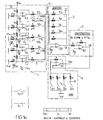
- FIG. 1a A more detailed description of a converter digital / analog self-programming at runtime immediate, in accordance with the subject of the present invention, will now be given with reference to FIG. 1a in a nonlimiting embodiment.
- the digital / analog converter receives a digital value to be converted, coded on N bits, the coding bits being denoted b 0 , for the least significant bit, to b N-1 for the most significant bit, the current bit being noted b j .
- the analog voltage generated is designated by V OUT .
- the value of this analog voltage is, by definition, between the electrical supply voltage Vcc and a reference voltage, denoted V REF also designated by ground voltage.
- the digital / analog converter object of the present invention comprises circuits 1 programmable generators of an image electric current, denoted I i , proportional to the sum of the active values of electric voltages of a sequence of N electric voltages constituting a geometric progression of reason 1 ⁇ 2.
- the sequence of N electrical voltages forms an analog image of the weight of the coding bits of the digital value to be converted between the most significant bit b N-1 and the least significant bit b 0 on which the digital value to be converted is coded or represented.
- the sequence of N electric voltages constituting a geometric progression of reason 1 ⁇ 2 preferably checks the relation (1):
- V j Vcc / 2 nj
- each active value of electric voltage denoted Vx j .
- Vx j b j .Vcc / 2 nj .
- the active values of electric voltages for the value of the bits b j equal to the value 1, are equal to the corresponding value of the analog image of the weight of the bits represented by the corresponding electric voltage of the following the N electrical voltages constituting the geometric progression, while, for the zero value of these bits, the corresponding active value is of course equal to zero.
- the digital / analog converter object of the invention, comprises first circuits 2 programmable correctors receiving the image electric current I i proportional to the sum of the active values of the above-mentioned electric voltages, these first circuits 2 making it possible to generate a first programmed corrected analog voltage, denoted V A proportional to the difference between the supply voltage Vcc and the weighted sum of the active values of electric voltages of the series of electric voltages represented by the electric current image I i cited above.
- the weighting term of the weighted sum is inversely proportional to the number of bits ⁇ to the value 1 of the digital value to be converted.
- the digital / analog converter object of the invention, further comprises second correcting circuits 3 receiving the first corrected programmed analog voltage V A and making it possible to generate a second voltage corrected analog programmed V B substantially equal in magnitude and as a sign to the weighted sum of the active values of electric voltages of the series of electric voltages.
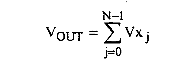
- the digital / analog converter object of the invention, as shown in FIG. 1a, comprises third correcting circuits 4 receiving the second programmed corrected analog voltage V B and making it possible to apply a programmed gain equal to the inverse of the weighting term, these third correcting circuits 4 thus making it possible to generate the analog voltage V OUT with a value comprised between the supply voltage Vcc and the reference voltage V REF and whose value is equal to the sum of the active voltage values of the sequence of electrical voltages according to relation (2).
- a preferred embodiment may consist in constructing the programmable generator circuits 1 so that it includes, with reference to the figure 1a, at least a plurality, denoted 10, of N electrical voltage dividing bridges connected in cascade between the supply voltage and the reference voltage.
- the plurality of dividing bridges has been shown as constituted by bridges R 0 / 2R 0 , R 0 designating a determined resistance value.
- each successive divider bridge is connected to the midpoint of the divider bridge of neighboring rank, the midpoint of each divider bridge of rank j given thus delivering an electrical voltage of value Vcc / 2 Nj constituting the series of values of electrical voltages .
- the programmable generator circuits 1 comprise, as shown in FIG. 1a, a plurality, denoted 11, of N series circuits, N being here equal to 4, each formed by a resistance of determined value, which can of course be distinct of the value R 0 previously mentioned in the description, and by a switch noted SW 0 , SW j , ..., SW N-1 , these switches being of course programmable in open values, respectively closed as a function of the value of one of the bits b 0 to b N-1 constituting the digital value to be converted.
- the least significant bit LSB that is to say the bit b 0
- the most significant bit MSB that is to say the bit b 3
- the input terminal of each series circuit is connected to the midpoint of one of the successive dividing bridges. In a preferred nonlimiting version, this connection, as shown in FIG.
- separating amplifier 1a is made by means of a separating amplifier, denoted A 0 , ..., A j to A 3 , this separating amplifier having as its object to separate each series circuit from the successive dividing bridges to which they are connected in order to avoid any harmful electrical interaction, the separating amplifiers A j being able to have a very low output impedance and a very high input impedance, so as to achieve this function of seperation.
- the embodiment of these separating amplifiers will not be described in detail since it corresponds to an embodiment known to those skilled in the art.
- each series circuit receives an electric voltage of value Vcc / 2 Nj and delivers, as a function of the programmed position, closed or open, from the corresponding switch SW j , by the corresponding bit b j at the value 1 or 0 of the digital value to be converted, an elementary image electric current, noted I ij , which is proportional to the voltage value Vcc / 2 Nj .
- the value of each elementary image electric current I ij corresponds to an active value of the electric voltages of the sequence of electric voltages for a bit of value 1 and an elementary image electric current of zero value corresponds to a non-active value of the electric voltages of the series of electrical voltages for a bit of value zero.
- each elementary image electric current I ij is proportional to the aforementioned active value, which verifies the relation (2) previously mentioned in the description.
- the output terminal of each of the signals constituting the plurality of series circuits is connected in parallel to deliver the previously mentioned image electric current I i , sum of the elementary image currents I ij .
- the image electric current I i is proportional to the sum of the active values of the above-mentioned electric voltages.
- each elementary image electric current and consequently the image electric current is proportional to the inverse of the resistance R constituting each series circuit.
- the latter may include, as shown in FIG. 1 a, an operational amplifier, noted 20, the terminal of which negative input is mounted in virtual pseudo-ground terminal and receives the image electric current I i delivered by the circuits 1 programmable generators.
- the positive input terminal of the amplifier operational 20 is itself connected to a so-called voltage offset, preferably taken equal to half the supply voltage Vcc.
- the output of the operational amplifier 20 delivers, for programming each of the programmable switches in the closed or open position, depending on the value of the bits b 0 to b N-1 of the digital value to be converted, the first corrected analog voltage programmed V A.
- the weighted sum of the active values of electric voltages is defined by a weighting term inversely proportional to the number of bits at the value 1 of the numerical value to be converted, as will be explained in more detail in the description.
- the second correcting circuits 3 taking into account the value of the first programmed corrected analog voltage V A , these, with reference to FIG. 1a, can advantageously include an operational amplifier 30 whose negative terminal is mounted in virtual pseudo-ground terminal and receives the first programmed corrected analog voltage V A via a resistance of determined value equal to the value R mentioned above.
- the output of the operational amplifier 30 is connected in feedback by a resistor of the same value to the negative terminal of this same operational amplifier 30.
- the positive terminal of the latter is connected to an offset voltage equal to the half of the supply voltage Vcc.
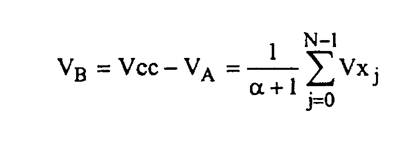
- the output of the operational amplifier 30 delivers, from the first programmed corrected analog voltage V A , the second programmed corrected analog voltage V B substantially equal in magnitude and as a sign to the weighted sum of the active values of the following electrical voltages.
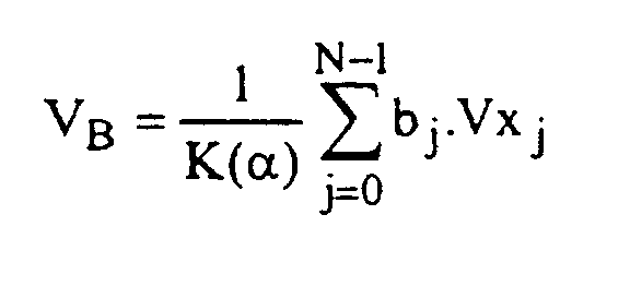
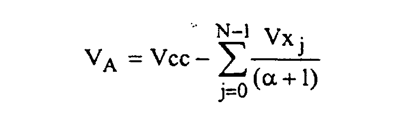
- the second programmed corrected analog voltage V B checks the relationship:
- K ( ⁇ ) weighting coefficient
- ⁇ denoting the number of bits equal to the value 1 of the numeric value to convert.
- third corrector circuits 4 thereof may include, considering the value of the second, corrected analogue voltage programmed V B, an operational amplifier 40 gain corrector which negative terminal is connected to the reference voltage V REF via a plurality of N series circuits each formed by a resistor of the same value, the value R, and by a programmable switch ensuring the same function as the programmable switches SW 0 , SW j to SW 3 previously mentioned in the description.
- the output terminal of the operational amplifier being connected in feedback to the negative terminal of the operational amplifier 40 by means of a resistor of the same value R
- the positive terminal of the operational amplifier 40 connected to the output of the second correcting circuits 3, receives the second programmed corrected analog voltage V B.
- the output of the operational amplifier 40 delivers by application of an inverse gain of the weighting term, that is to say a gain of the form K ( ⁇ ), at the second programmed corrected analog voltage, the analog output voltage denoted V OUT , the value of which is thus equal to the sum of the active values of electric voltages of the series of electric voltages.
- this termination divider bridge makes it possible to deliver, from the last aforementioned voltage value, another voltage value in the ratio 1 ⁇ 2 with respect to the previous one and which thus constitutes a value proportional to half the least significant bit LSB weight value.
- the voltage value delivered by the bridge R 0 / R 0 becomes Vcc / 32.
- the image current I i advantageously comprises an offset value, denoted I id , proportional to half the value of the weight of the least bit significant.
- This value is introduced as a permanent active pseudo-value in order to shift the zero value of the analog voltage obtained by a very low value which can be made as low as the value of the supply voltage Vcc divided by the power of two of the number of bits + 1 on which the digital value to be converted is coded.
- each plurality of series circuits, programmable generator circuits 1 and correcting circuits 2 further comprises a resistor, which may be permanent, of the same value R, connected directly in parallel to all of the corresponding series circuits.
- a resistor which may be permanent, of the same value R
- the resistor such as the permanent resistor R represented in FIG. 1a, is connected via a separating amplifier A at the midpoint of the aforementioned R 0 / R 0 termination bridge.
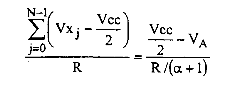
- V AT - Vcc / 2 R Vcc / 2 - V B R
- the device, object of the present invention, as described, thus makes it possible to obtain an analog voltage equal to the sum of the active values Vx j of the electric voltages of the above-mentioned series of electric voltages.
- the introduction of the offset value through permanent value resistors R represented in FIG. 1a can be understood as the introduction of a pseudo-bit of value 1, not relative to the encoded numeric value to be converted but relative to the value of the analog voltage finally obtained.
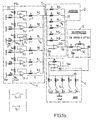
- a permanent resistor R can be added or, if appropriate, a pseudo-bit, denoted b -2 .
- the transcoding at the zero value of the pseudo-bit b -1 makes it possible to reduce to an operation similar to that of FIG. 1a in which, however, the offset value of voltage of analog voltage is no longer equal to half the value of the least significant bit, but to a quarter.
- the digital / analog converter object of the present invention, makes it possible to provide for operation on a variable number of bits , the number of bits thus being able to be brought to a value N + 2, the pseudo-bits b -1 and b -2 being able to participate effectively in the conversion of a value coded on N + 1 bits.
- the number of serial circuits of the plurality of serial circuits, both in the programmable generator circuits 1 and the first correcting circuits 2 is not limited.
Landscapes
- Engineering & Computer Science (AREA)
- Theoretical Computer Science (AREA)
- Analogue/Digital Conversion (AREA)
- Amplifiers (AREA)
- Networks Using Active Elements (AREA)
Description
Il comporte enfin des troisièmes circuits correcteurs recevant la deuxième tension analogique corrigée programmée et permettant d'appliquer un gain programmé, égal à l'inverse du terme de pondération, ceci permettant d'engendrer la tension analogique comprise entre la tension d'alimentation et la tension de référence, valeur égale à la somme des valeurs actives de tensions électriques de la suite de tensions électriques.
- la figure 1a représente, à titre d'exemple non limitatif, un premier exemple de réalisation du convertisseur numérique/analogique, objet de la présente invention ;
- la figure 1b représente, à titre d'exemple non limitatif, un deuxième exemple de réalisation du convertisseur numérique/analogique, objet de la présente invention.


Claims (6)
- Convertisseur numérique/analogique à exécution immédiate, recevant une valeur numérique à convertir, codée sur N bits, en une tension analogique de valeur comprise entre une tension électrique d'alimentation Vcc et une tension de référence, tension de masse, comportant :caractérisé en ce qu'il comporte au moins:des moyens générateurs programmables d'un courant électrique image proportionnel à la somme des valeurs actives de tensions électriques d'une suite de N tensions électriques constituant une progression géométrique de raison ½ et formant une image analogique du poids des bits entre le bit le plus significatif et le bit le moins significatif sur lesquels ladite valeur numérique à convertir est codée, lesdites valeurs actives correspondant auxdites valeurs de tensions électriques de cette suite de valeurs pour lesquelles l'image analogique du poids des bits de ladite valeur numérique à convertir correspond à un bit de valeur 1 ;des premiers moyens correcteurs programmables recevant ledit courant électrique image et permettant d'engendrer une première tension analogique corrigée programmée proportionnelle à la différence entre ladite tension d'alimentation Vcc et la somme pondérée desdites valeurs actives de tensions électriques de la suite de tensions électriques, le terme de pondération de ladite somme pondérée étant inversement proportionnel au nombre de bits à la valeur 1 de ladite valeur numérique à convertir ;des deuxièmes moyens correcteurs recevant ladite première tension analogique corrigée programmée et permettant d'engendrer une deuxième tension analogique corrigée programmée sensiblement égale en grandeur et en signe à ladite somme pondérée desdites valeurs actives de tensions électriques de ladite suite de tensions électriques ;des troisièmes moyens correcteurs recevant ladite deuxième tension analogique corrigée programmée et permettant d'appliquer un gain programmé, égal à l'inverse dudit terme de pondération, ce qui permet d'engendrer ladite tension analogique de valeur comprise entre ladite tension d'alimentation et ladite tension de référence, valeur égale à la somme desdites valeurs actives de tensions électriques de ladite suite de tensions électriques.
- Convertisseur numérique/analogique selon la revendication 1, caractérisé en ce que lesdits moyens générateurs programmables d'un courant image proportionnel à la somme des valeurs actives de tensions électriques comportent au moins :une pluralité de N ponts diviseurs de tension électrique R0/2R0 connectés en cascade, entre ladite tension d'alimentation et ladite tension de référence, R désignant une valeur de résistance déterminée, la borne d'entrée du premier pont diviseur étant connectée à la tension d'alimentation Vcc et la borne d'entrée de chaque pont diviseur successif étant connectée au point milieu du pont diviseur de rang voisin, le point milieu de chaque pont diviseur de rang j délivrant une tension électrique de valeur Vcc/2N-j constitutive de la suite de valeurs de tensions électriques ;une pluralité de N circuits série, formés chacun par une résistance de valeur déterminée et un interrupteur programmable(b0, bj à b3), la borne d'entrée de chaque circuit série étant connectée au point milieu d'un pont diviseur et recevant une tension électrique de valeur Vcc/2N-j, chaque circuit série délivrant, en fonction de la position programmée fermée ou ouverte de cet interrupteur, par un bit à la valeur 1 ou 0 de ladite valeur numérique à convertir, un courant électrique image élémentaire Iij proportionnel à ladite valeur Vcc/2N-j, correspondant à une valeur active des tensions électriques de ladite suite de tensions électriques pour un bit de valeur 1, et un courant électrique image élémentaire de valeur nulle, correspondant à une valeur non active des tensions électriques de la suite de tensions électriques pour un bit de valeur 0, la borne de sortie de ladite pluralité de circuits série étant connectée en parallèle, pour délivrer ledit courant électrique image Ii, somme des courants image élémentaires Iij, proportionnel à la somme desdites valeurs actives de tensions électriques.
- Convertisseur numérique/analogique selon l'une des revendications 1 ou 2, caractérisé en ce que lesdits premiers moyens correcteurs programmables comprennent un amplificateur opérationnel dont la borne d'entrée négative, montée en borne de pseudo-masse virtuelle reçoit ledit courant électrique image Ii délivré par lesdits moyens générateurs programmables, la borne de sortie dudit amplificateur opérationnel étant connectée en contre-réaction à ladite borne négative par l'intermédiaire d'une pluralité de N circuits série formés chacun par une résistance de même valeur et un interrupteur programmable, l'ensemble des N circuits série étant connectés en parallèle, la borne d'entrée positive dudit amplificateur opérationnel étant connectée à une tension de décalage, égale à la moitié de la tension d'alimentation, la sortie dudit amplificateur opérationnel délivrant, pour une programmation de chacun des interrupteurs programmables en position fermée ou ouverte, en fonction de la valeur des bits de ladite valeur numérique à convertir, ladite première tension analogique corrigée programmée VA.
- Convertisseur numérique/analogique selon l'une des revendications 1 à 3, caractérisé en ce que lesdits deuxièmes moyens correcteurs comprennent un amplificateur opérationnel dont la borne négative, montée en borne de pseudo-masse virtuelle, reçoit ladite première tension analogique corrigée programmée VA, par l'intermédiaire d'une résistance de valeur déterminée, la sortie dudit amplificateur opérationnel étant connectée en contre-réaction par une résistance de même valeur à ladite borne négative, la borne positive dudit amplificateur opérationnel étant connectée à une tension de décalage égale à la moitié de la tension d'alimentation, la sortie dudit amplificateur opérationnel délivrant ladite deuxième tension analogique corrigée programmée VB sensiblement égale en grandeur et en signe à ladite somme pondérée desdites valeurs actives de ladite suite de tensions électriques.
- Convertisseur numérique/analogique selon l'une des revendications 1 à 4, caractérisé en ce que lesdits troisièmes moyens correcteurs comprennent un amplificateur opérationnel correcteur de gain, dont la borne négative est connectée à ladite tension de référence, tension de masse, par l'intermédiaire d'une pluralité de N circuits série formés chacun par une résistance de même valeur et un interrupteur programmable, l'ensemble des N circuits série étant connectés en parallèle, la borne de sortie dudit amplificateur opérationnel étant connectée en contre-réaction à ladite borne négative par une résistance de même valeur, la borne positive dudit amplificateur opérationnel étant connectée à la sortie desdits deuxièmes moyens correcteurs et recevant ladite deuxième tension analogique corrigée programmée VB, la sortie dudit amplificateur opérationnel délivrant, par application d'un gain inverse du terme de pondération à ladite deuxième tension analogique corrigée programmée, ladite tension analogique VOUT de valeur égale à la somme desdites valeurs actives de tensions électriques de ladite suite de tensions électriques.
- Convertisseur numérique/analogique selon l'une des revendications précédentes, caractérisé en ce que pour une valeur numérique à convertir codée sur N bits, ledit courant image Ii comporte une valeur de décalage proportionnelle à la moitié de la valeur du poids du bit le moins significatif, cette valeur étant introduite comme pseudo-valeur active permanente, chaque pluralité de circuit série des moyens générateurs programmables et des premiers moyens correcteurs comportant en outre une résistance permanente de même valeur connectée directement en parallèle sur l'ensemble des circuits série, le terme de pondération étant inversement proportionnel au nombre de bits à la valeur 1 de ladite valeur numérique à convertir augmenté de 1 et le terme de gain étant proportionnel au nombre de bits à la valeur 1 augmenté de 1, de ladite valeur numérique à convertir.
Applications Claiming Priority (3)
| Application Number | Priority Date | Filing Date | Title |
|---|---|---|---|
| FR9911827 | 1999-09-22 | ||
| FR9911827A FR2798792B1 (fr) | 1999-09-22 | 1999-09-22 | Convertisseur numerique/analogique autoprogrammable a execution immediate |
| PCT/FR2000/002617 WO2001022596A1 (fr) | 1999-09-22 | 2000-09-21 | Convertisseur numerique/analogique |
Publications (2)
| Publication Number | Publication Date |
|---|---|
| EP1131890A1 EP1131890A1 (fr) | 2001-09-12 |
| EP1131890B1 true EP1131890B1 (fr) | 2004-11-03 |
Family
ID=9550110
Family Applications (1)
| Application Number | Title | Priority Date | Filing Date |
|---|---|---|---|
| EP00964339A Expired - Lifetime EP1131890B1 (fr) | 1999-09-22 | 2000-09-21 | Convertisseur numerique/analogique |
Country Status (6)
| Country | Link |
|---|---|
| US (1) | US6414617B1 (fr) |
| EP (1) | EP1131890B1 (fr) |
| AT (1) | ATE281711T1 (fr) |
| DE (1) | DE60015494T2 (fr) |
| FR (1) | FR2798792B1 (fr) |
| WO (1) | WO2001022596A1 (fr) |
Families Citing this family (2)
| Publication number | Priority date | Publication date | Assignee | Title |
|---|---|---|---|---|
| US9595974B1 (en) * | 2014-09-08 | 2017-03-14 | Lockheed Martin Corporation | Reconfigurable wideband sub-ranging analog-to-digital converter |
| CN116260465A (zh) * | 2023-03-21 | 2023-06-13 | 上海米硅科技有限公司 | 数模转换器输出电路及数模转换器 |
Family Cites Families (4)
| Publication number | Priority date | Publication date | Assignee | Title |
|---|---|---|---|---|
| JPS59160319A (ja) * | 1983-03-02 | 1984-09-11 | Nippon Gakki Seizo Kk | Daコンバ−タ |
| JPH03255722A (ja) * | 1990-03-06 | 1991-11-14 | Nec Corp | D/a変換器 |
| GB2333408A (en) * | 1998-01-17 | 1999-07-21 | Sharp Kk | Non-linear digital-to-analog converter |
| US6307490B1 (en) * | 1999-09-30 | 2001-10-23 | The Engineering Consortium, Inc. | Digital to analog converter trim apparatus and method |
-
1999
- 1999-09-22 FR FR9911827A patent/FR2798792B1/fr not_active Expired - Fee Related
-
2000
- 2000-09-21 DE DE60015494T patent/DE60015494T2/de not_active Expired - Lifetime
- 2000-09-21 WO PCT/FR2000/002617 patent/WO2001022596A1/fr not_active Ceased
- 2000-09-21 EP EP00964339A patent/EP1131890B1/fr not_active Expired - Lifetime
- 2000-09-21 AT AT00964339T patent/ATE281711T1/de not_active IP Right Cessation
- 2000-09-21 US US09/856,330 patent/US6414617B1/en not_active Expired - Lifetime
Also Published As
| Publication number | Publication date |
|---|---|
| FR2798792A1 (fr) | 2001-03-23 |
| US6414617B1 (en) | 2002-07-02 |
| DE60015494D1 (de) | 2004-12-09 |
| ATE281711T1 (de) | 2004-11-15 |
| WO2001022596A1 (fr) | 2001-03-29 |
| DE60015494T2 (de) | 2005-10-20 |
| EP1131890A1 (fr) | 2001-09-12 |
| FR2798792B1 (fr) | 2001-11-16 |
Similar Documents
| Publication | Publication Date | Title |
|---|---|---|
| FR2911737A1 (fr) | Procede pour numeriser une grandeur analogique, dispositif de numerisation mettant en oeuvre ce procede et detecteur de rayonnements electromagnetiques integrant un tel dispositif | |
| FR2509048A1 (fr) | Dispositif transducteur de pression capacitif a caracteristique lineaire | |
| FR2722040A1 (fr) | Circuit d'accord | |
| FR2689706A1 (fr) | Convertisseur numérique-analogique comportant un tampon de sortie à tension de décalage ajustable. | |
| EP0421896B1 (fr) | Convertisseur analogique/numérique à haute fréquence de conversion | |
| EP0278534B1 (fr) | Déphaseur large bande | |
| EP0606799A1 (fr) | Convertisseur analogique numérique avec échantillonneur bloqueur distribué | |
| EP1131890B1 (fr) | Convertisseur numerique/analogique | |
| EP2978127B1 (fr) | Procédé de compensation numérique des variations, en fonction de la température, d'une grandeur électrique d'un équipement de télécommunications radiofréquence spatial embarqué | |
| FR2791490A1 (fr) | Dispositif de conversion analogique/numerique a non-linearite differentielle constante | |
| EP0011534B1 (fr) | Procédé et dispositif de traitement d'un signal analogique, notamment pseudopériodique | |
| EP0463964B1 (fr) | Système d'émission-réception d'ultrasons | |
| EP0065901A1 (fr) | Système potentiométrique perfectionné | |
| EP0230809A1 (fr) | Caméra thermique à balayage parallèle | |
| EP0071505A1 (fr) | Procédé et dispositif pour l'échantillonnage d'un signal sinusoidal par un signal de fréquence multiple | |
| EP0195709B1 (fr) | Générateur numérique de forme d'onde et procédé associé | |
| EP0749234B1 (fr) | Capteur d'image à semi-conducteur à transformation intégrée d'histogramme de pixels | |
| FR2711792A1 (fr) | Dispositif de mesure de flux lumineux. | |
| FR2843250A1 (fr) | Convertisseur numerique-analogique comprenant des moyens pour ameliorer la linearite de conversion. | |
| FR2762162A1 (fr) | Dispositif d'alignement numerique | |
| EP4057514B1 (fr) | Dispositif de conversion numerique analogique a fort rapport signal/bruit | |
| EP1076417B1 (fr) | Circuit de répliement de signal, et cellule d'interpolation série d'un convertisseur analogique-numérique utilisant un tel circuit | |
| EP1975633A1 (fr) | Dispositif de mesure d`une charge électrique sous forme numérisée | |
| FR2723277A1 (fr) | Convertisseur analogique-numerique et systeme de conversion analogique-numerique mettant en oeuvre ledit convertisseur | |
| FR2755325A1 (fr) | Dispositif de conversion analogique/numerique a caracteristique de transfert programmable |
Legal Events
| Date | Code | Title | Description |
|---|---|---|---|
| PUAI | Public reference made under article 153(3) epc to a published international application that has entered the european phase |
Free format text: ORIGINAL CODE: 0009012 |
|
| 17P | Request for examination filed |
Effective date: 20010525 |
|
| AK | Designated contracting states |
Kind code of ref document: A1 Designated state(s): AT BE CH CY DE DK ES FI FR GB GR IE IT LI LU MC NL PT SE |
|
| AX | Request for extension of the european patent |
Free format text: AL;LT;LV;MK;RO;SI |
|
| GRAP | Despatch of communication of intention to grant a patent |
Free format text: ORIGINAL CODE: EPIDOSNIGR1 |
|
| RTI1 | Title (correction) |
Free format text: DIGITAL-TO-ANALOG CONVERTER |
|
| GRAS | Grant fee paid |
Free format text: ORIGINAL CODE: EPIDOSNIGR3 |
|
| GRAA | (expected) grant |
Free format text: ORIGINAL CODE: 0009210 |
|
| AK | Designated contracting states |
Kind code of ref document: B1 Designated state(s): AT BE CH CY DE DK ES FI FR GB GR IE IT LI LU MC NL PT SE |
|
| PG25 | Lapsed in a contracting state [announced via postgrant information from national office to epo] |
Ref country code: IE Free format text: LAPSE BECAUSE OF FAILURE TO SUBMIT A TRANSLATION OF THE DESCRIPTION OR TO PAY THE FEE WITHIN THE PRESCRIBED TIME-LIMIT Effective date: 20041103 Ref country code: FI Free format text: LAPSE BECAUSE OF FAILURE TO SUBMIT A TRANSLATION OF THE DESCRIPTION OR TO PAY THE FEE WITHIN THE PRESCRIBED TIME-LIMIT Effective date: 20041103 Ref country code: AT Free format text: LAPSE BECAUSE OF FAILURE TO SUBMIT A TRANSLATION OF THE DESCRIPTION OR TO PAY THE FEE WITHIN THE PRESCRIBED TIME-LIMIT Effective date: 20041103 |
|
| REG | Reference to a national code |
Ref country code: GB Ref legal event code: FG4D Free format text: NOT ENGLISH |
|
| REG | Reference to a national code |
Ref country code: CH Ref legal event code: EP |
|
| REF | Corresponds to: |
Ref document number: 60015494 Country of ref document: DE Date of ref document: 20041209 Kind code of ref document: P |
|
| REG | Reference to a national code |
Ref country code: IE Ref legal event code: FG4D Free format text: FRENCH |
|
| PG25 | Lapsed in a contracting state [announced via postgrant information from national office to epo] |
Ref country code: SE Free format text: LAPSE BECAUSE OF FAILURE TO SUBMIT A TRANSLATION OF THE DESCRIPTION OR TO PAY THE FEE WITHIN THE PRESCRIBED TIME-LIMIT Effective date: 20050203 Ref country code: DK Free format text: LAPSE BECAUSE OF FAILURE TO SUBMIT A TRANSLATION OF THE DESCRIPTION OR TO PAY THE FEE WITHIN THE PRESCRIBED TIME-LIMIT Effective date: 20050203 Ref country code: GR Free format text: LAPSE BECAUSE OF FAILURE TO SUBMIT A TRANSLATION OF THE DESCRIPTION OR TO PAY THE FEE WITHIN THE PRESCRIBED TIME-LIMIT Effective date: 20050203 |
|
| PG25 | Lapsed in a contracting state [announced via postgrant information from national office to epo] |
Ref country code: ES Free format text: LAPSE BECAUSE OF FAILURE TO SUBMIT A TRANSLATION OF THE DESCRIPTION OR TO PAY THE FEE WITHIN THE PRESCRIBED TIME-LIMIT Effective date: 20050214 |
|
| GBT | Gb: translation of ep patent filed (gb section 77(6)(a)/1977) |
Effective date: 20050224 |
|
| REG | Reference to a national code |
Ref country code: IE Ref legal event code: FD4D |
|
| PLBE | No opposition filed within time limit |
Free format text: ORIGINAL CODE: 0009261 |
|
| STAA | Information on the status of an ep patent application or granted ep patent |
Free format text: STATUS: NO OPPOSITION FILED WITHIN TIME LIMIT |
|
| PG25 | Lapsed in a contracting state [announced via postgrant information from national office to epo] |
Ref country code: CY Free format text: LAPSE BECAUSE OF FAILURE TO SUBMIT A TRANSLATION OF THE DESCRIPTION OR TO PAY THE FEE WITHIN THE PRESCRIBED TIME-LIMIT Effective date: 20050921 |
|
| PG25 | Lapsed in a contracting state [announced via postgrant information from national office to epo] |
Ref country code: MC Free format text: LAPSE BECAUSE OF NON-PAYMENT OF DUE FEES Effective date: 20050930 Ref country code: LU Free format text: LAPSE BECAUSE OF NON-PAYMENT OF DUE FEES Effective date: 20050930 Ref country code: LI Free format text: LAPSE BECAUSE OF NON-PAYMENT OF DUE FEES Effective date: 20050930 Ref country code: CH Free format text: LAPSE BECAUSE OF NON-PAYMENT OF DUE FEES Effective date: 20050930 Ref country code: BE Free format text: LAPSE BECAUSE OF NON-PAYMENT OF DUE FEES Effective date: 20050930 |
|
| 26N | No opposition filed |
Effective date: 20050804 |
|
| REG | Reference to a national code |
Ref country code: CH Ref legal event code: PL |
|
| BERE | Be: lapsed |
Owner name: S.A. *ATMEL NANTES Effective date: 20050930 |
|
| PG25 | Lapsed in a contracting state [announced via postgrant information from national office to epo] |
Ref country code: PT Free format text: LAPSE BECAUSE OF NON-PAYMENT OF DUE FEES Effective date: 20050403 |
|
| PGFP | Annual fee paid to national office [announced via postgrant information from national office to epo] |
Ref country code: GB Payment date: 20090904 Year of fee payment: 10 Ref country code: NL Payment date: 20090818 Year of fee payment: 10 |
|
| PGFP | Annual fee paid to national office [announced via postgrant information from national office to epo] |
Ref country code: IT Payment date: 20090919 Year of fee payment: 10 |
|
| REG | Reference to a national code |
Ref country code: NL Ref legal event code: V1 Effective date: 20110401 |
|
| GBPC | Gb: european patent ceased through non-payment of renewal fee |
Effective date: 20100921 |
|
| PG25 | Lapsed in a contracting state [announced via postgrant information from national office to epo] |
Ref country code: IT Free format text: LAPSE BECAUSE OF NON-PAYMENT OF DUE FEES Effective date: 20100921 |
|
| PG25 | Lapsed in a contracting state [announced via postgrant information from national office to epo] |
Ref country code: NL Free format text: LAPSE BECAUSE OF NON-PAYMENT OF DUE FEES Effective date: 20110401 Ref country code: GB Free format text: LAPSE BECAUSE OF NON-PAYMENT OF DUE FEES Effective date: 20100921 |
|
| PGFP | Annual fee paid to national office [announced via postgrant information from national office to epo] |
Ref country code: FR Payment date: 20121001 Year of fee payment: 13 |
|
| REG | Reference to a national code |
Ref country code: DE Ref legal event code: R082 Ref document number: 60015494 Country of ref document: DE Representative=s name: GRUENECKER, KINKELDEY, STOCKMAIR & SCHWANHAEUS, DE |
|
| PGFP | Annual fee paid to national office [announced via postgrant information from national office to epo] |
Ref country code: DE Payment date: 20130918 Year of fee payment: 14 |
|
| REG | Reference to a national code |
Ref country code: DE Ref legal event code: R082 Ref document number: 60015494 Country of ref document: DE Representative=s name: GRUENECKER, KINKELDEY, STOCKMAIR & SCHWANHAEUS, DE Effective date: 20131023 Ref country code: DE Ref legal event code: R081 Ref document number: 60015494 Country of ref document: DE Owner name: ATMEL CORPORATION, US Free format text: FORMER OWNER: ATMEL NANTES S.A., NANTES, FR Effective date: 20131023 Ref country code: DE Ref legal event code: R081 Ref document number: 60015494 Country of ref document: DE Owner name: ATMEL CORPORATION, SAN JOSE, US Free format text: FORMER OWNER: ATMEL NANTES S.A., NANTES, FR Effective date: 20131023 Ref country code: DE Ref legal event code: R082 Ref document number: 60015494 Country of ref document: DE Representative=s name: GRUENECKER PATENT- UND RECHTSANWAELTE PARTG MB, DE Effective date: 20131023 |
|
| REG | Reference to a national code |
Ref country code: FR Ref legal event code: ST Effective date: 20140530 |
|
| PG25 | Lapsed in a contracting state [announced via postgrant information from national office to epo] |
Ref country code: FR Free format text: LAPSE BECAUSE OF NON-PAYMENT OF DUE FEES Effective date: 20130930 |
|
| REG | Reference to a national code |
Ref country code: DE Ref legal event code: R119 Ref document number: 60015494 Country of ref document: DE |
|
| PG25 | Lapsed in a contracting state [announced via postgrant information from national office to epo] |
Ref country code: DE Free format text: LAPSE BECAUSE OF NON-PAYMENT OF DUE FEES Effective date: 20150401 |