EP1132964A2 - Anordnung zur Verschaltung von Leistungshalbleiterchips in Modulen - Google Patents
Anordnung zur Verschaltung von Leistungshalbleiterchips in Modulen Download PDFInfo
- Publication number
- EP1132964A2 EP1132964A2 EP01104998A EP01104998A EP1132964A2 EP 1132964 A2 EP1132964 A2 EP 1132964A2 EP 01104998 A EP01104998 A EP 01104998A EP 01104998 A EP01104998 A EP 01104998A EP 1132964 A2 EP1132964 A2 EP 1132964A2
- Authority
- EP
- European Patent Office
- Prior art keywords
- power semiconductor
- semiconductor chips
- module
- modules
- chips
- Prior art date
- Legal status (The legal status is an assumption and is not a legal conclusion. Google has not performed a legal analysis and makes no representation as to the accuracy of the status listed.)
- Withdrawn
Links
Images
Classifications
-
- H—ELECTRICITY
- H10—SEMICONDUCTOR DEVICES; ELECTRIC SOLID-STATE DEVICES NOT OTHERWISE PROVIDED FOR
- H10W—GENERIC PACKAGES, INTERCONNECTIONS, CONNECTORS OR OTHER CONSTRUCTIONAL DETAILS OF DEVICES COVERED BY CLASS H10
- H10W90/00—Package configurations
-
- H—ELECTRICITY
- H10—SEMICONDUCTOR DEVICES; ELECTRIC SOLID-STATE DEVICES NOT OTHERWISE PROVIDED FOR
- H10W—GENERIC PACKAGES, INTERCONNECTIONS, CONNECTORS OR OTHER CONSTRUCTIONAL DETAILS OF DEVICES COVERED BY CLASS H10
- H10W72/00—Interconnections or connectors in packages
- H10W72/50—Bond wires
- H10W72/541—Dispositions of bond wires
- H10W72/547—Dispositions of multiple bond wires
- H10W72/5475—Dispositions of multiple bond wires multiple bond wires connected to common bond pads at both ends of the wires
-
- H—ELECTRICITY
- H10—SEMICONDUCTOR DEVICES; ELECTRIC SOLID-STATE DEVICES NOT OTHERWISE PROVIDED FOR
- H10W—GENERIC PACKAGES, INTERCONNECTIONS, CONNECTORS OR OTHER CONSTRUCTIONAL DETAILS OF DEVICES COVERED BY CLASS H10
- H10W90/00—Package configurations
- H10W90/701—Package configurations characterised by the relative positions of pads or connectors relative to package parts
- H10W90/751—Package configurations characterised by the relative positions of pads or connectors relative to package parts of bond wires
- H10W90/754—Package configurations characterised by the relative positions of pads or connectors relative to package parts of bond wires between a chip and a stacked insulating package substrate, interposer or RDL
Definitions
- the present invention relates to an arrangement for interconnection of power semiconductor chips in modules where the power semiconductor chips at least two different ones Assigned function types and each via ceramic substrates are applied to a common base plate.
- IGBT bipolar transistor with isolated Gate
- IGBT bipolar transistor with isolated Gate
- DCB "sandwich substrate” copper-ceramic-copper.
- the ceramic substrates in turn are preferred soldered to a base plate.
- the ceramic substrate takes over in particular DCB, the function of an electrical one Isolation and thermal conduction in the power semiconductor chip arising heat. Also includes the ceramic substrate structures associated with bonded wires the electrical function of the power semiconductor chip realize.
- the base plate serves as a support mechanically and thermally as a heat capacity and heat conductor to one if necessary additionally provided heat sink on which the power semiconductor module is screwed.
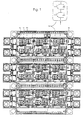
- IGBT power semiconductor chips and diode power semiconductor chips checkered pattern on the individual Substrates as well as overall on the bottom plate in the Module provided.
- Power semiconductor chips of the same Function types occupy fields of the same Color of the checkerboard pattern.
- IGBT power semiconductor chips are for example on "black” Fields provided while diode power semiconductor chips assigned to the "white” fields are.
- individual power semiconductor chips are in in the form of IGBT chips 1 and diode chips 2 over substrates 3 applied to a base plate 4 and in the manner of a checkerboard pattern arranged.
- substrates 3 preferably DCB used.
- Half bridges 4 Basic electrical functions are on the substrates 3 as Half bridges 4 realized and by means of a bus system 5 and corresponding bond wires connected in parallel to each other. To simplify the illustration, there are only one bus system at a time 5 and a half-bridge 4 particularly highlighted.
- individual substrates can be cut by current measuring resistors be replaced.
- additional functions that is, current measurements in, for example, linearly guided phase lines possible.
- Rectifier input bridges instead of individual substrates in the module can be installed.
Landscapes
- Power Conversion In General (AREA)
- Cooling Or The Like Of Semiconductors Or Solid State Devices (AREA)
- Semiconductor Integrated Circuits (AREA)
Abstract
Description
Claims (3)
- Anordnung zur Verschaltung von Leistungshalbleiterchips (1, 2) in Modulen, bei der die Leistungshalbleiterchips (1, 2) wenigstens zwei verschiedenen Funktionstypen zugeordnet und auf eine gemeinsame Bodenplatte (4) aufgebracht sind,
dadurch gekennzeichnet, daßdie Leistungshalbleiterchips (1, 2) schachbrettmusterartig angeordnet sind und möglichst gleiche Funktionstypen Felder der gleichen Farbe des Schachbrettmusters besetzen,die Leistungshalbleiterchips (1, 2) jeweils über keramische Substrate (3) aus DCB auf der gemeinsamen Bodenplatte (4) aufgebracht sind, undin dem Schachbrettmuster ein Bussystem symmetrisch angeordnet ist. - Anordnung nach Anspruch 1,
dadurch gekennzeichnet, daß
die Funktionstypen durch IGBT's und Leistungsdioden gegeben sind. - Anordnung nach Anspruch 1 oder 2,
dadurch gekennzeichnet, daß
Grundfunktionen des Moduls auf jeweils einem der Substrate (3) realisiert sind.
Applications Claiming Priority (2)
| Application Number | Priority Date | Filing Date | Title |
|---|---|---|---|
| DE10011633 | 2000-03-10 | ||
| DE10011633A DE10011633A1 (de) | 2000-03-10 | 2000-03-10 | Anordnung zur Verschaltung von Leistungshalbleiterchips in Modulen |
Publications (2)
| Publication Number | Publication Date |
|---|---|
| EP1132964A2 true EP1132964A2 (de) | 2001-09-12 |
| EP1132964A3 EP1132964A3 (de) | 2003-11-12 |
Family
ID=7634187
Family Applications (1)
| Application Number | Title | Priority Date | Filing Date |
|---|---|---|---|
| EP01104998A Withdrawn EP1132964A3 (de) | 2000-03-10 | 2001-03-01 | Anordnung zur Verschaltung von Leistungshalbleiterchips in Modulen |
Country Status (3)
| Country | Link |
|---|---|
| US (1) | US20010026434A1 (de) |
| EP (1) | EP1132964A3 (de) |
| DE (1) | DE10011633A1 (de) |
Families Citing this family (8)
| Publication number | Priority date | Publication date | Assignee | Title |
|---|---|---|---|---|
| DE10316356B4 (de) | 2003-04-10 | 2012-07-26 | Semikron Elektronik Gmbh & Co. Kg | Modular aufgebautes Leistungshalbleitermodul |
| DE10317018A1 (de) * | 2003-04-11 | 2004-11-18 | Infineon Technologies Ag | Multichipmodul mit mehreren Halbleiterchips sowie Leiterplatte mit mehreren Komponenten |
| WO2009093982A1 (en) | 2008-01-25 | 2009-07-30 | Iskralab D.O.O. | Power switching module |
| CN111048491B (zh) | 2012-03-01 | 2023-04-18 | 三菱电机株式会社 | 电力用半导体模块以及电力变换装置 |
| DE102015103667A1 (de) * | 2015-03-12 | 2016-09-15 | Infineon Technologies Bipolar Gmbh & Co. Kg | Leistungshalbleitermodul mit verbesserter Bondverbindungstruktur |
| CN113126703B (zh) * | 2020-01-14 | 2023-09-08 | 戴尔产品有限公司 | 电力传输系统 |
| CN113270374A (zh) * | 2021-04-30 | 2021-08-17 | 深圳芯能半导体技术有限公司 | Igbt功率器件 |
| CN116487337A (zh) * | 2023-05-31 | 2023-07-25 | 中国振华集团永光电子有限公司(国营第八七三厂) | 一种三相全桥igbt模块及其制作方法 |
Family Cites Families (4)
| Publication number | Priority date | Publication date | Assignee | Title |
|---|---|---|---|---|
| DE59107655D1 (de) * | 1991-02-22 | 1996-05-09 | Asea Brown Boveri | Abschaltbares Hochleistungs-Halbleiterbauelement |
| DE9313483U1 (de) * | 1993-09-07 | 1994-01-05 | SZE Microelectronics GmbH, 24220 Flintbek | Vorrichtung zur Aufnahme |
| EP0884781A3 (de) * | 1997-06-12 | 1999-06-30 | Hitachi, Ltd. | Leistungshalbleitermodul |
| JP3786320B2 (ja) * | 1997-09-29 | 2006-06-14 | 株式会社デンソー | モータ駆動用のインバータモジュール |
-
2000
- 2000-03-10 DE DE10011633A patent/DE10011633A1/de not_active Ceased
-
2001
- 2001-03-01 EP EP01104998A patent/EP1132964A3/de not_active Withdrawn
- 2001-03-12 US US09/803,759 patent/US20010026434A1/en not_active Abandoned
Also Published As
| Publication number | Publication date |
|---|---|
| EP1132964A3 (de) | 2003-11-12 |
| US20010026434A1 (en) | 2001-10-04 |
| DE10011633A1 (de) | 2001-09-20 |
Similar Documents
| Publication | Publication Date | Title |
|---|---|---|
| EP3942603B1 (de) | Elektronischer schaltkreis und verfahren zur herstellung eines elektronischen schaltkreises | |
| DE102012213407B4 (de) | Halbleiteranordnung | |
| DE102015101086B4 (de) | Leistungshalbleitermodulanordnung | |
| DE10393437T5 (de) | Halbleiterbauelementbaugruppe | |
| DE19900603A1 (de) | Elektronisches Halbleitermodul | |
| DE102007013186A1 (de) | Halbleitermodul mit Halbleiterchips und Verfahren zur Herstellung desselben | |
| DE102010002627A1 (de) | Niederinduktive Leistungshalbleiterbaugruppe | |
| DE102018112477A1 (de) | Halbleiterpackage mit leiterrahmen | |
| DE112016005574B4 (de) | Halbleitermodule | |
| EP0750345B1 (de) | Leistungs-Halbleitermodul | |
| DE102007046969B3 (de) | Elektronische Schaltung aus Teilschaltungen und Verfahren zu deren Herstellung und demgemäßer Umrichter oder Schalter | |
| DE212020000459U1 (de) | Halbleiterbauteil | |
| DE112020006374T5 (de) | Leistungsmodul mit verbesserten elektrischen und thermischen Charakteristiken | |
| EP1083599A2 (de) | Leistungshalbleitermodul | |
| DE102020127327A1 (de) | Gestapeltes Transistorchip-Package mit Source-Kopplung | |
| DE212020000458U1 (de) | Halbleiterbauteil | |
| DE102019112936A1 (de) | Halbleitermodul | |
| DE102018216399B4 (de) | Verfahren zum Herstellen eines Leistungs-Halbleitermoduls und Leistungs-Halbleitermodul | |
| DE60306040T2 (de) | Halbleitermodul und Leistungswandlervorrichtung | |
| EP1132964A2 (de) | Anordnung zur Verschaltung von Leistungshalbleiterchips in Modulen | |
| DE102023208490A1 (de) | Leistungselektronikmodul und Montageverfahren | |
| DE10101777A1 (de) | Einzelmodulsystem für elektrisches/elektronisches Gerät | |
| EP3949103A1 (de) | Elektronische schaltungseinheit | |
| DE112023004856T5 (de) | Elektronische vorrichtung mit einem chip, der zwischen einem ersten und einem zweiten substrat angeordnet ist | |
| DE102005049978A1 (de) | Schaltungsanordnung für Tiefsetzsteller und Verfahren zur Herstellung eines Leistungs-Halbleiterbauelements |
Legal Events
| Date | Code | Title | Description |
|---|---|---|---|
| PUAI | Public reference made under article 153(3) epc to a published international application that has entered the european phase |
Free format text: ORIGINAL CODE: 0009012 |
|
| AK | Designated contracting states |
Kind code of ref document: A2 Designated state(s): AT BE CH CY DE DK ES FI FR GB GR IE IT LI LU MC NL PT SE TR |
|
| AX | Request for extension of the european patent |
Free format text: AL;LT;LV;MK;RO;SI |
|
| PUAL | Search report despatched |
Free format text: ORIGINAL CODE: 0009013 |
|
| AK | Designated contracting states |
Kind code of ref document: A3 Designated state(s): AT BE CH CY DE DK ES FI FR GB GR IE IT LI LU MC NL PT SE TR |
|
| AX | Request for extension of the european patent |
Extension state: AL LT LV MK RO SI |
|
| RIC1 | Information provided on ipc code assigned before grant |
Ipc: 7H 01L 25/11 B Ipc: 7H 01L 25/07 A |
|
| AKX | Designation fees paid | ||
| REG | Reference to a national code |
Ref country code: DE Ref legal event code: 8566 |
|
| STAA | Information on the status of an ep patent application or granted ep patent |
Free format text: STATUS: THE APPLICATION IS DEEMED TO BE WITHDRAWN |
|
| 18D | Application deemed to be withdrawn |
Effective date: 20040513 |