EP1133166A2 - Verdoppeln des X-dimension eines Videorahmens mit Hardware - Google Patents
Verdoppeln des X-dimension eines Videorahmens mit Hardware Download PDFInfo
- Publication number
- EP1133166A2 EP1133166A2 EP00311371A EP00311371A EP1133166A2 EP 1133166 A2 EP1133166 A2 EP 1133166A2 EP 00311371 A EP00311371 A EP 00311371A EP 00311371 A EP00311371 A EP 00311371A EP 1133166 A2 EP1133166 A2 EP 1133166A2
- Authority
- EP
- European Patent Office
- Prior art keywords
- data
- image
- display
- image data
- original amount
- Prior art date
- Legal status (The legal status is an assumption and is not a legal conclusion. Google has not performed a legal analysis and makes no representation as to the accuracy of the status listed.)
- Withdrawn
Links
Images



Classifications
-
- H—ELECTRICITY
- H04—ELECTRIC COMMUNICATION TECHNIQUE
- H04N—PICTORIAL COMMUNICATION, e.g. TELEVISION
- H04N1/00—Scanning, transmission or reproduction of documents or the like, e.g. facsimile transmission; Details thereof
- H04N1/46—Colour picture communication systems
- H04N1/64—Systems for the transmission or the storage of the colour picture signal; Details therefor, e.g. coding or decoding means therefor
- H04N1/646—Transmitting or storing colour television type signals, e.g. PAL, Lab; Their conversion into additive or subtractive colour signals or vice versa therefor
-
- H—ELECTRICITY
- H04—ELECTRIC COMMUNICATION TECHNIQUE
- H04N—PICTORIAL COMMUNICATION, e.g. TELEVISION
- H04N23/00—Cameras or camera modules comprising electronic image sensors; Control thereof
- H04N23/60—Control of cameras or camera modules
- H04N23/63—Control of cameras or camera modules by using electronic viewfinders
Definitions
- This invention relates in general to using a computer hardware based scheme for doubling the X-dimension in a video frame such as that used in a Liquid Crystal Display (LCD) of a stand-alone digital still camera.
- LCD Liquid Crystal Display
- Display of captured image data may be provided on a variety of devices such as Liquid Crystal Display (LCD) or Cathode Ray Tube (CRT) display devices.
- LCD Liquid Crystal Display
- CRT Cathode Ray Tube
- captured image data is most often displayed on a built-in LCD screen for proposes of previewing materials, inspecting post-capture images, etcetera.
- External CRT devices may also be supported for purposes of visually sharing images with others.
- the captured image data of such cameras may be in various formats, such as RGB (red, green, blue format) or YCrCb format.
- a converter such as a National Television System Committee (NTSC) converter, Systeme Electronique Couleur Avec Memoire (SECAM) converter, or Phase Alteration by Line (PAL) converter, may be utilized for encoding the data to an appropriate video standard. Displaying data in this manner has an advantage over LCDs utilizing a direct digital interface in that it permits common drive signals to an internal LCD or a CRT device external to the stand-alone camera.
- NTSC converters are standardized 8-bit devices based on a so-called YCrCb 4:2:2 format wherein 4 complete pixels will consist of four "Y" (luminance) bytes of data, two Cr (chrominance) bytes of data and two Cb (chrominance) bytes of data.
- this format yields twice as much luminance data as chrominance data, all of which is represented according to the 4:2:2 ratio, the shorthand for which is represented as YCrCb 4:2:2.
- Bus bandwidth usually defined as the maximum amount of data that may be transferred over the system bus in a one second period of time, is always finite. In a typical digital still camera, bus bandwidth may have a theoretical limit on the order of a few tens of megabytes per second, and in practice will be less than this due to the arbitration time required to hand the bus off to various system modules. Since up to 29.5 megabytes per second on a limited bandwidth requires an intolerably high portion of the total bandwidth available, this necessarily compromises the availability of the bus to function in the camera.
- a stand-alone digital camera operating in preview mode one is necessarily constantly exposing the CCD to capture an image, while simultaneously doing image processing (e.g., demosaicing, filtering, color correction, etc.) on each image and sending data to the LCD for display.
- image processing e.g., demosaicing, filtering, color correction, etc.
- Most, if not all, of these functions require either writing image data across the bus to the SDRAM (e.g., for the CCD control module), reading data across the bus from the SDRAM (e.g., for the LCD control module), or both (e.g., for the CPU and image processing modules).
- Such preview function is particularly taxing on the system because unlike other functions, such as post-capture and post-view mode, multiple tasks are required simultaneously. Thus, particularly where the system is trying to multitask, as it necessarily does when utilizing the capturing, storing and processing modes simultaneously, the prior art level of performance is unacceptable.
- the image stored in the SDRAM could be half as big as that required by the NTSC/PAL/SECAM encoder, for example.
- the CPU would still have to read this image out of SDRAM, upsample it to the required size, and send it to the display module over the system bus.
- such an approach actually requires more bus bandwidth.
- a desire for a system and method for efficiently communicating captured image data between components of a stand-alone digital camera that is, a desire exists for a system and method that allows for captured image data to be communicated along a system bus to various components of a digital camera, without requiring an unnecessarily large amount of bandwidth. For example, it is desirable to reduce the bandwidth required for communicating image data within a digital camera when operating in a mode that requires multi-tasking, such as a preview mode.
- a system and method that efficiently communicates image data within a digital camera, while still providing a sufficient amount of data to a display, such as a LCD, for an acceptable display quality.
- a preferred embodiment provides a hardware based implementation, which can reduce the bandwidth usage in a stand-alone digital still image camera when transmitting a data stream to an encoder (e.g., a NTSC/PAL/SECAM encoder) for the purpose of displaying an image on a LCD display and/or a CRT.
- an encoder e.g., a NTSC/PAL/SECAM encoder
- the above goals are accomplished through the use of a particular internal logic configuration in a display block equipped with registers.
- the configuration of the particular display block is structured on an Application Specific Integrated Circuit (ASIC) scheme so as to interact with a NTSC/PAL/SECAM encoder in such a manner as to minimize the bandwidth requirements of the display block while presenting data at the necessary rate to an NTSC/PAL/SECAM encoder.
- ASIC Application Specific Integrated Circuit
- the X-dimension data is halved, and the image data having a halved X-dimension is communicated within the camera for processing, thereby reducing the bandwidth required for communicating the image data along the camera's system bus.
- a display block e.g., Display Module
- a "doubling module” doubles the X-dimension to provide the data stream expected by the encoder and display (e.g., LCD).
- the impact on the bandwidth of the camera's system bus is minimized by manipulation of the YCrCb 4:2:2 data format so as to halve the X-direction data before communicating the image data along the system bus, and then "double" the X-direction data presented to the display block prior to passing it to the NTSC/PAL encoder.
- This has the effect of reducing (halving) the amount of data transmitted to the display block, thereby reducing the impact on the system bus bandwidth for running the LCD.
- a technical advantage of one aspect of the present invention is that a system and method for reducing the bandwidth required for communicating captured image data along a stand-alone digital camera's system bus are provided. That is, the communication of image data along a system bus for running a LCD (or other display) is accomplished in a manner that has a minimal impact on the system bus bandwidth. Accordingly, the impact on the bandwidth when communicating image data in a multi-tasking operation mode, for example, is minimized.
- a further technical advantage of one aspect of the present invention is that the image data is provided to an encoder and display with sufficient data to allow for display of an image having an acceptable quality. Thus, captured image data may be communicated along a camera's system bus in an efficient manner, while still providing an acceptable quality image to the camera's display.
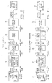
- FIGURE 1 shows a block diagram of the hardware system 100 used in a stand-alone digital still camera of a preferred embodiment of the present invention.
- This system is comprised of an image capture device 1 (preferably a CCD or CMOS sensor); an analog-to-digital (A/D) converter 2; ASIC 10 which preferably includes an image capture control module 3, CPU 4, image processing module 5, memory controller module 7, system bus 6, and display module 11; a memory device 9 (preferably SDRAM), which is connected to ASIC 10 via bus 8; an encoder 13 (preferably NTSC/PAL format, although may be another format such as SECAM); and a display device 14 (preferably LCD). Additionally, a provision is made for displaying an image on TV or CRT 16, which is external to the system, via the video out signal 15.
- ASIC 10 which preferably includes an image capture control module 3, CPU 4, image processing module 5, memory controller module 7, system bus 6, and display module 11
- a memory device 9 preferably SDRAM
- an encoder 13 preferably NTSC/PAL format, although may be another format such
- the above-detailed elements are provided with specific interconnection therebetween.
- the image capture device 1 and A/D converter 2 for converting the captured analog signals to digital signals are connected directly to the ASIC 10 via digital data bus 22 and A/D control bus 21.
- the output of the image capture device 1 is connected directly to the input of the A/D converter 2.
- the output of the A/D converter 2 is connected directly to the ASIC 10 by means of a digital data bus 22, whose width is dependent on the resolution of A/D converter 2.
- this digital data enters the ASIC 10 at image capture control module 3.
- the image capture control module 3 controls the A/D converter 2 and the image capture device 1.
- Communication between the memory controller 7 and memory device 9 is via memory bus 8.
- Communication between the display module 11 and the encoder module 13 is via NTSC control bus 12.
- the encoder module 13 drives the display device 14 and/or an optional TV/CRT device 16 via the analog video out signal 15.
- connection link 12 is preferably a NTSC control bus, which is most preferably a 24.5-29.5 megabyte/second digital-type bus.
- Encoder module 13 is connected to display device 14 and optional TV/CRT device 16 via connection link 15 (preferably composite video out 15).
- an image i.e., video/image data
- the hardware of a preferred embodiment operates in the following fashion: an image (i.e., video/image data) is captured by the image capture device 1.
- an image capture device 1 a sampled analog signal is then passed to the A/D converter 2 to be converted to a digital signal ("the data") which is transmitted to ASIC 10 via communication link 22, and passes through image capture control module 3.
- the image capture control module 3 optionally manipulates data for quality purposes prior to passing it through memory controller 7 to memory device 9 via bus 8.
- Alternative embodiments of the present invention also contemplate further retrieving the stored data from memory device 9 for processing within the CPU 4 and other units, but the preferred embodiment, in its simplest sense, provides for a peripheral role of the CPU 4 in the overall scheme.
- image processing module 5 is in communication with CPU 4 via system bus 6.
- a preferred embodiment of the described system and method is preferably a hardware instantiation because a similarly fashioned software approach must still send the whole image across the system bus 6 because the image is processed in the CPU 4.
- system bus bandwidth problems of the prior art are alleviated.
- display module 11 retrieves the data out of memory device 8 via bus connection link 6 for temporary residence therein.
- the internal logic 17 is critical to the preferred embodiment because the YCrCb 4:2:2 format requires quantitatively and qualitatively more logic to output the data which comes out in the target sequence.
- the internal logic 17 is purposely structured as to produce output in the required sequence, specifically, the internal logic will double the X-dimension (i.e., "X * 2") of the data stream which has been processed, in the various stages, through image capture control module 3, CPU 4 and image processing module 5, all of which are inter-connected via system bus 6.
- the X-dimension is doubled because, during processing, e.g., via CPU 4, the X-dimension is "halved" (i.e., "X/2") so that, when passing through system bus 6, the reduced X-dimension reduces the bandwidth required therein as indicated within modules 18, 19 and 20.
- this drops every other column of data, thereby reducing bandwidth. Therefore, the internal logic 17 doubles the X-dimension data to allow for the data to be in the sequence expected by the encoder module 13.
- One of image capture control module 3, CPU 4, image processing 5, will have an X-dimension halving module shown as X/2 18, 19, 20 for reducing the data input stream.
- There are two methods for halving the X-dimension data the first is to halve the data prior to storage in the memory device. This halving would be performed by the halving module 18 in the image capture control module 3.
- the X-dimension data would be halved prior to inputting the data on system bus 6 and storage in memory device 9 through memory controller 7. This would result in a greatly reduced bus bandwidth usage as both inputting and retrieving from memory device 9 would have reduced bandwidth usage.
- the other method is to store all of the X-dimension data in memory device 9 and use either CPU 4 or image processing module 5 with halving modules 19, 20 to reduce the X-dimension data.
- Halving modules 19, 20 may reduce the data and re-store that data to memory device 9 for later retrieval for display on the built-in display device 14 and/or TV/CRT device 16.
- the resulting data having a halved X-dimension is stored in memory device 9 separate from the full resolution data originally captured and stored therein. Reducing the data in this manner allows for reduced bandwidth for system bus 6, while providing the required amount of data at NTSC bus 12 at the time of display.
- one of halving modules 19, 20 could halve the X-dimension data as it is being retrieved from memory device 9 for other purposes prior to delivery to display module 11. Reducing the data in this manner allows for reduced bandwidth during a portion of the transfer of data across system bus 6, i.e., the bandwidth is reduced as it is being transferred to memory module 11. Note that in a preferred embodiment only one halving module 18, 19, or 20 is needed in ASIC 10 as this function would only need to be carried out once on the data.
- FIGURE 2 is a conceptual representation of various color formats for a four pixel, two-dimensional image.
- FIGURE 2 depicts equivalent representations in different color spaces (i.e., different color formats).
- the image capture device 1 may capture an image as RGB data, in which after demosaicing and/or other processing each Red is represented at 32 (R 1 , R 2 , R 3 and R 4 ), each green represented at 34 (G 1 , G 2 , G 3 and G 4 ), and each Blue represented at 36 (B 1 , B 2 , B 3 and B 4 ).
- RGB data is typically translated into a format such as YCrCb 4:4:4 shown at 38, which details the illuminance values at 40 (Y 1 , Y 2 , Y 3 and Y 4 ) and chrominances at 42 (Cb 1 , Cb 2 , C b3 and C b4 ) and at 44 (Cr 1 , Cr 2 , Cr 3 and Cr 4 ), all of which are in groupings of the two-dimensional, four pixel images (i.e., each box represents one byte of data).
- YCrCb 4:4:4 the same number of bytes are required to represent an image in YCrCb 4:4:4 format as are required for RGB format.
- YCrCb 4:2:2 format includes illuminance values 46 (Y 1 , Y 2 , Y 3 and Y 4 ), chrominance values 48 (Cb 1 and Cb 3 ), and chrominance values 50 (Cr 1 and Cr 3 ), all of which are in groupings according to the two-dimensional, four pixels images (i.e., each box represents one byte of data).
- the image data in YCrCb 4:2:2 format having size NxM is communicated from Memory Device 62 across system bus 64 to Display Module 66, then further across bus 68 to NTSC/PAL Encoder 70 which sends a composite analog signal out 72 to NxM LCD display 74.
- a preferred embodiment of the present invention specifically allows for data captured by the image capture device 1 as RGB data to be converted to YCrCb 4:2:2.
- the process of a preferred embodiment is illustrated in the context of hardware blocks shown in FIGURE 4 where the image capture device 78 captures the data in RGB format according to the number of N pixels by M lines (for an image size of NxM) and communicates the captured RGB data across bus 80 to Image Transformation and Resizing module 82.
- the image data is then converted to YCrCb 4:2:2 data format having (N/2)xM size. That is, the X-dimension of the data is divided in half, thereby reducing the amount of data required to be communicated over the system bus to various hardware blocks of the system.
- the image data having size (N/2)xM is communicated through bus 84 to Memory Device 86, wherein the image data is stored. Thereafter, the image data having size (N/2)xM is communicated across system bus 88 to Display Module 90.
- the image data is then transformed to size NxM. That is, the X-doubling module 91 doubles the X-dimension of the image data, resulting in the NxM size of data expected by the Encoder 94 and LCD display 98.
- Display Module 90 then communicates the image data having size NxM across bus 92 to NTSC/PAL Encoder 94, which sends a composite analog signal out 96 to NxM LCD display 98.
- the respective processing of the systems described above will yield the byte streams represented in FIGURES 5 and 6.
- the prior art display processing 100 will send the byte stream at 102 of Cb 1 , Y 1 , Cr 1 , Y 2 , Cb 3 Y 3 Cr 3 , Y 4 , Cb 5 ...Cb n-1 , Y n-1 , Cr n-1 , Y n into Display Module 104 and will result in the byte stream 106, which is Cb 1 , Y 1 , Cr 1 , Y 2 , Cb 3 ,Y 3 Cr 3 , Y 3 , Cr 3 , Y 3 , Cb 5 ...Cb n-1 , Y n-1 , Cr n-1 , Y n , all of which are 2n bytes of output per n pixel LCD line.
- the sequence of bytes 102 communicated across the system bus as input to Display Module 104 are 2n bytes of output per n
- FIGURE 6 depicts the X-doubling display processing where byte stream 110, which represents n bytes of input data per n pixel LCD line is represented as Cb' 1 , Y' 1 , Cr' 1 , Y' 2 , Cb' 3 , Y' 3 , Cr' 3 , Y' 4 ...
- bandwidth usage is necessarily reduced via the n/2 inventive methodology, given that the prior art byte stream involves 2n bytes of input data per n pixel LCD line, while the inventive byte stream 110 simply entails n bytes of input data per n pixel LCD line. This results, of course, in a smaller quantity of bytes which need to be transmitted across system bus 6. Additionally, feeding the data 110 through X-doubling logic unit 116 results in a data stream 114 which is 2n bytes of output data per n pixel LCD line.
- the data stream from display Module 112 will resemble data stream 114, which will have a fundamental base unit called quad (e.g., quad 113) which is determined in sequence by a successive "Y.'"
- quad e.g., quad 113
- Y' 1 will describe the first quad 113
- Y' 2 will describe the second quad
- Y' 3 the third quad
- each successive Y' 1 value will be doubled so as to make up for the value not present in the n bytes of data input stream 110.
- the "Cb"' values will be repeated (i.e., in a preferred embodiment, the system will utilize only two instances of chrominance values, Cb' 1 and Cb' 3 , rather than the four instances of Cb' 1 , Cb' 2 , Cb' 3 and Cb' 4 ) and the pattern of which is likewise repeated for the "Cr" values.
- the bytes will comprise Cb' 1 , Y' 1 , Cr' 1 (indicated at 115), and having Y' 1 repeated or doubled (indicated at 117) will comprise the total quad 113 (i.e., Cb' 1 , Y' 1 , Cr' 1 , Y' 1) .
- This technique is repeated at next data quad 118, which is dictated by the next successive "Y'” (i.e., Y' 2 ) and repeats the same "Cb"' and "Cr”' value as previously indicated (i.e., the system repeats "Cb' 1 " and "Cr' 1 ").
- this technique is utilized in Preview mode of a camera, wherein a user previews an image using a built-in display device (e.g., a LCD device). It will be recalled from the above discussion that it is desirable to reduce the bandwidth usage during such a preview operation because of the multi-tasking that is performed in that mode.
- a preferred embodiment utilizes the method of halving the X-dimension to transfer image data across the system bus during preview mode, thereby reducing the amount of bandwidth required for the image data during such a multi-tasking mode.
- the system may be implemented to utilize this method to reduce the required bandwidth during any mode of operation, and the scope of the present invention is intended to encompass any such implementation.
- Provision for X-doubling is provided in a preferred embodiment according to the above-described manner, but nevertheless, if one were, say, to provide pixel 1, pixel 3, pixel 1, pixel 3 within the above-described methodology, certain adverse effects might be propagated, such as ghosted images, etcetera. Notwithstanding this, it is possible for alternative embodiments to utilize other techniques such as sampling (odd, even, pairing, etc.) combined with filtering (low pass, etc.) as known in the art of sampling and filtering, in conjunction with the above methodology. As such, the alternating pixel replication process described above eliminates much of the redundancy called for by the NTSC encoder 13 from being communicated across the system bus 6.
Landscapes
- Engineering & Computer Science (AREA)
- Multimedia (AREA)
- Signal Processing (AREA)
- Digital Computer Display Output (AREA)
- Color Television Systems (AREA)
- Transforming Electric Information Into Light Information (AREA)
- Processing Of Color Television Signals (AREA)
- Studio Devices (AREA)
- Controls And Circuits For Display Device (AREA)
Applications Claiming Priority (2)
| Application Number | Priority Date | Filing Date | Title |
|---|---|---|---|
| US47768700A | 2000-01-06 | 2000-01-06 | |
| US477687 | 2000-01-06 |
Publications (2)
| Publication Number | Publication Date |
|---|---|
| EP1133166A2 true EP1133166A2 (de) | 2001-09-12 |
| EP1133166A3 EP1133166A3 (de) | 2003-08-06 |
Family
ID=23896928
Family Applications (1)
| Application Number | Title | Priority Date | Filing Date |
|---|---|---|---|
| EP00311371A Withdrawn EP1133166A3 (de) | 2000-01-06 | 2000-12-19 | Verdoppeln des X-dimension eines Videorahmens mit Hardware |
Country Status (2)
| Country | Link |
|---|---|
| EP (1) | EP1133166A3 (de) |
| JP (1) | JP2001238117A (de) |
Family Cites Families (5)
| Publication number | Priority date | Publication date | Assignee | Title |
|---|---|---|---|---|
| GB8630887D0 (en) * | 1986-12-24 | 1987-02-04 | Philips Electronic Associated | Encoding & displaying pictures |
| CA1261069A (en) * | 1986-12-08 | 1989-09-26 | Mohamed S. Sabri | Two-channel coding of digital signals |
| US4774562A (en) * | 1987-06-02 | 1988-09-27 | Eastman Kodak Company | Image transmission system with preview mode |
| US5596659A (en) * | 1992-09-01 | 1997-01-21 | Apple Computer, Inc. | Preprocessing and postprocessing for vector quantization |
| US5453844A (en) * | 1993-07-21 | 1995-09-26 | The University Of Rochester | Image data coding and compression system utilizing controlled blurring |
-
2000
- 2000-12-19 EP EP00311371A patent/EP1133166A3/de not_active Withdrawn
- 2000-12-25 JP JP2000392276A patent/JP2001238117A/ja active Pending
Also Published As
| Publication number | Publication date |
|---|---|
| EP1133166A3 (de) | 2003-08-06 |
| JP2001238117A (ja) | 2001-08-31 |
Similar Documents
| Publication | Publication Date | Title |
|---|---|---|
| US6348925B1 (en) | Method and apparatus for block data transfer to reduce on-chip storage for interpolative video resizing | |
| US20120194735A1 (en) | System And Method For An Image Sensor Operable In Multiple Video Standards | |
| JP2004515981A (ja) | 携帯電話用の最適化されたカメラセンサ構造 | |
| JP2002111989A (ja) | 画像処理回路 | |
| US7701466B2 (en) | Method and system for providing accelerated video processing in a communication device | |
| KR100483191B1 (ko) | 전자 줌기능을 갖는 디지털 카메라 및 이미지 처리방법 | |
| EP1575278A1 (de) | Mobiles endgerät mit kamera | |
| EP2008238A1 (de) | Verfahren zur erleichterung der verwendung kleinzeiliger puffer zur bearbeitung kleiner oder grosser bilder | |
| US20050190270A1 (en) | Method and apparatus for processing image signal | |
| US11431941B2 (en) | Method, apparatus, and system for processing digital images | |
| US7212214B2 (en) | Apparatuses and methods for interpolating missing colors | |
| KR101016490B1 (ko) | 화상 데이터의 변환 방법 및 변환 회로와, 전자 카메라 | |
| US7236194B2 (en) | Image signal processing apparatus | |
| US20020074481A1 (en) | Dual-mode CMOS integrated imager | |
| WO2001011460A1 (en) | System and method for producing a video signal | |
| US20030080984A1 (en) | Method and apparatus for digital image processing | |
| CN101175193B (zh) | 图像信号产生单元、数码相机以及图像信号产生方法 | |
| US6348950B1 (en) | Video signal processing circuit and image pickup apparatus using the circuit | |
| US20070065022A1 (en) | Image signal processing apparatus and method | |
| EP1133166A2 (de) | Verdoppeln des X-dimension eines Videorahmens mit Hardware | |
| US6646686B1 (en) | Managing alpha values for video mixing operations | |
| EP1401203A1 (de) | Verfahren zum realisieren einer kombination von mehrfachmengen mehrerer digitaler bilder und busschnittstellentechnik | |
| KR100486494B1 (ko) | 디지털스틸카메라의데이터전송장치및방법 | |
| KR20050094445A (ko) | 프레임 변환 방법, 프레임 변환 회로 및 전자 카메라 | |
| JPH0944634A (ja) | 映像入力装置 |
Legal Events
| Date | Code | Title | Description |
|---|---|---|---|
| PUAI | Public reference made under article 153(3) epc to a published international application that has entered the european phase |
Free format text: ORIGINAL CODE: 0009012 |
|
| AK | Designated contracting states |
Kind code of ref document: A2 Designated state(s): AT BE CH CY DE DK ES FI FR GB GR IE IT LI LU MC NL PT SE TR |
|
| AX | Request for extension of the european patent |
Free format text: AL;LT;LV;MK;RO;SI |
|
| PUAL | Search report despatched |
Free format text: ORIGINAL CODE: 0009013 |
|
| AK | Designated contracting states |
Designated state(s): AT BE CH CY DE DK ES FI FR GB GR IE IT LI LU MC NL PT SE TR |
|
| AX | Request for extension of the european patent |
Extension state: AL LT LV MK RO SI |
|
| RIC1 | Information provided on ipc code assigned before grant |
Ipc: 7H 04N 5/232 B Ipc: 7H 04N 1/41 B Ipc: 7H 04N 1/64 A |
|
| 17P | Request for examination filed |
Effective date: 20031020 |
|
| 17Q | First examination report despatched |
Effective date: 20031229 |
|
| AKX | Designation fees paid |
Designated state(s): GB |
|
| REG | Reference to a national code |
Ref country code: DE Ref legal event code: 8566 |
|
| STAA | Information on the status of an ep patent application or granted ep patent |
Free format text: STATUS: THE APPLICATION IS DEEMED TO BE WITHDRAWN |
|
| 18D | Application deemed to be withdrawn |
Effective date: 20050701 |