EP1138683A2 - Composé du bore, procédé pour le préparer, et dispositif organique électroluminescent le contenant - Google Patents
Composé du bore, procédé pour le préparer, et dispositif organique électroluminescent le contenant Download PDFInfo
- Publication number
- EP1138683A2 EP1138683A2 EP01108056A EP01108056A EP1138683A2 EP 1138683 A2 EP1138683 A2 EP 1138683A2 EP 01108056 A EP01108056 A EP 01108056A EP 01108056 A EP01108056 A EP 01108056A EP 1138683 A2 EP1138683 A2 EP 1138683A2
- Authority
- EP
- European Patent Office
- Prior art keywords
- compound
- organic
- formula
- layer
- represented
- Prior art date
- Legal status (The legal status is an assumption and is not a legal conclusion. Google has not performed a legal analysis and makes no representation as to the accuracy of the status listed.)
- Granted
Links
- 238000004020 luminiscence type Methods 0.000 title claims abstract description 90
- 150000001639 boron compounds Chemical class 0.000 title claims abstract description 37
- 238000000034 method Methods 0.000 title claims abstract description 17
- 230000008569 process Effects 0.000 title claims abstract description 17
- 150000001875 compounds Chemical class 0.000 title claims description 59
- -1 aromatic ketone compound Chemical class 0.000 claims abstract description 68
- 125000000623 heterocyclic group Chemical group 0.000 claims abstract description 24
- 125000000217 alkyl group Chemical group 0.000 claims abstract description 17
- 125000003118 aryl group Chemical group 0.000 claims abstract description 14
- 125000002924 primary amino group Chemical group [H]N([H])* 0.000 claims abstract description 14
- 125000003710 aryl alkyl group Chemical group 0.000 claims abstract description 12
- 239000004327 boric acid Substances 0.000 claims abstract description 11
- 125000003545 alkoxy group Chemical group 0.000 claims abstract description 10
- 150000002367 halogens Chemical class 0.000 claims abstract description 9
- NLXLAEXVIDQMFP-UHFFFAOYSA-N Ammonia chloride Chemical compound [NH4+].[Cl-] NLXLAEXVIDQMFP-UHFFFAOYSA-N 0.000 claims abstract description 8
- 125000003435 aroyl group Chemical group 0.000 claims abstract description 8
- 125000002485 formyl group Chemical group [H]C(*)=O 0.000 claims abstract description 8
- 229910052736 halogen Inorganic materials 0.000 claims abstract description 8
- 150000002825 nitriles Chemical class 0.000 claims abstract description 8
- 125000003107 substituted aryl group Chemical group 0.000 claims abstract description 8
- 125000003342 alkenyl group Chemical group 0.000 claims abstract description 6
- 229910052739 hydrogen Inorganic materials 0.000 claims abstract description 5
- 239000001257 hydrogen Substances 0.000 claims abstract description 5
- 235000019270 ammonium chloride Nutrition 0.000 claims abstract description 4
- 150000002894 organic compounds Chemical class 0.000 claims description 19
- 125000001424 substituent group Chemical group 0.000 claims description 18
- HUMNYLRZRPPJDN-UHFFFAOYSA-N benzenecarboxaldehyde Natural products O=CC1=CC=CC=C1 HUMNYLRZRPPJDN-UHFFFAOYSA-N 0.000 claims description 4
- 125000004435 hydrogen atom Chemical class [H]* 0.000 claims description 4
- KGBXLFKZBHKPEV-UHFFFAOYSA-N boric acid Chemical compound OB(O)O KGBXLFKZBHKPEV-UHFFFAOYSA-N 0.000 claims description 3
- QNGNSVIICDLXHT-UHFFFAOYSA-N para-ethylbenzaldehyde Natural products CCC1=CC=C(C=O)C=C1 QNGNSVIICDLXHT-UHFFFAOYSA-N 0.000 claims description 3
- 239000002346 layers by function Substances 0.000 abstract description 3
- 150000002431 hydrogen Chemical class 0.000 abstract 1
- 239000010410 layer Substances 0.000 description 79
- QTBSBXVTEAMEQO-UHFFFAOYSA-N Acetic acid Chemical compound CC(O)=O QTBSBXVTEAMEQO-UHFFFAOYSA-N 0.000 description 24
- 239000000758 substrate Substances 0.000 description 20
- HEDRZPFGACZZDS-UHFFFAOYSA-N Chloroform Chemical compound ClC(Cl)Cl HEDRZPFGACZZDS-UHFFFAOYSA-N 0.000 description 18
- 239000000463 material Substances 0.000 description 15
- 238000001771 vacuum deposition Methods 0.000 description 14
- 235000019557 luminance Nutrition 0.000 description 13
- 238000006243 chemical reaction Methods 0.000 description 11
- 229920005989 resin Polymers 0.000 description 11
- 239000011347 resin Substances 0.000 description 11
- VQGHOUODWALEFC-UHFFFAOYSA-N 2-phenylpyridine Chemical compound C1=CC=CC=C1C1=CC=CC=N1 VQGHOUODWALEFC-UHFFFAOYSA-N 0.000 description 10
- KFZMGEQAYNKOFK-UHFFFAOYSA-N Isopropanol Chemical compound CC(C)O KFZMGEQAYNKOFK-UHFFFAOYSA-N 0.000 description 9
- USFZMSVCRYTOJT-UHFFFAOYSA-N Ammonium acetate Chemical compound N.CC(O)=O USFZMSVCRYTOJT-UHFFFAOYSA-N 0.000 description 8
- 239000005695 Ammonium acetate Substances 0.000 description 8
- 235000019257 ammonium acetate Nutrition 0.000 description 8
- 229940043376 ammonium acetate Drugs 0.000 description 8
- XLYOFNOQVPJJNP-UHFFFAOYSA-N water Substances O XLYOFNOQVPJJNP-UHFFFAOYSA-N 0.000 description 7
- UHOVQNZJYSORNB-UHFFFAOYSA-N Benzene Chemical compound C1=CC=CC=C1 UHOVQNZJYSORNB-UHFFFAOYSA-N 0.000 description 6
- 239000002244 precipitate Substances 0.000 description 6
- 238000003756 stirring Methods 0.000 description 6
- 0 c1c[n]c(-c2cc(-c(cccc3)c3O*3(c(cc4)ccc4-c4ccccc4)Oc4ccccc4-4)*3c-4c2)c1 Chemical compound c1c[n]c(-c2cc(-c(cccc3)c3O*3(c(cc4)ccc4-c4ccccc4)Oc4ccccc4-4)*3c-4c2)c1 0.000 description 5
- 230000001747 exhibiting effect Effects 0.000 description 5
- JVZRCNQLWOELDU-UHFFFAOYSA-N gamma-Phenylpyridine Natural products C1=CC=CC=C1C1=CC=NC=C1 JVZRCNQLWOELDU-UHFFFAOYSA-N 0.000 description 5
- 238000004519 manufacturing process Methods 0.000 description 5
- 229910052751 metal Inorganic materials 0.000 description 5
- 239000002184 metal Substances 0.000 description 5
- 125000001997 phenyl group Chemical group [H]C1=C([H])C([H])=C(*)C([H])=C1[H] 0.000 description 5
- ZUOUZKKEUPVFJK-UHFFFAOYSA-N diphenyl Chemical compound C1=CC=CC=C1C1=CC=CC=C1 ZUOUZKKEUPVFJK-UHFFFAOYSA-N 0.000 description 4
- 238000010438 heat treatment Methods 0.000 description 4
- 125000002496 methyl group Chemical group [H]C([H])([H])* 0.000 description 4
- 239000000203 mixture Substances 0.000 description 4
- JUJWROOIHBZHMG-UHFFFAOYSA-N pyridine Substances C1=CC=NC=C1 JUJWROOIHBZHMG-UHFFFAOYSA-N 0.000 description 4
- UMJSCPRVCHMLSP-UHFFFAOYSA-N pyridine Natural products COC1=CC=CN=C1 UMJSCPRVCHMLSP-UHFFFAOYSA-N 0.000 description 4
- 239000002356 single layer Substances 0.000 description 4
- 239000002904 solvent Substances 0.000 description 4
- 125000000999 tert-butyl group Chemical group [H]C([H])([H])C(*)(C([H])([H])[H])C([H])([H])[H] 0.000 description 4
- FNXGULSNFIUEMT-UHFFFAOYSA-N 2-[4-[4-(dimethylamino)phenyl]-6-(2-hydroxyphenyl)pyridin-2-yl]phenol Chemical compound C1=CC(N(C)C)=CC=C1C1=CC(C=2C(=CC=CC=2)O)=NC(C=2C(=CC=CC=2)O)=C1 FNXGULSNFIUEMT-UHFFFAOYSA-N 0.000 description 3
- 125000005427 anthranyl group Chemical group 0.000 description 3
- 239000011230 binding agent Substances 0.000 description 3
- 238000000576 coating method Methods 0.000 description 3
- 230000000052 comparative effect Effects 0.000 description 3
- 239000002019 doping agent Substances 0.000 description 3
- 230000000694 effects Effects 0.000 description 3
- 239000003480 eluent Substances 0.000 description 3
- 125000001495 ethyl group Chemical group [H]C([H])([H])C([H])([H])* 0.000 description 3
- 239000011521 glass Substances 0.000 description 3
- AMGQUBHHOARCQH-UHFFFAOYSA-N indium;oxotin Chemical compound [In].[Sn]=O AMGQUBHHOARCQH-UHFFFAOYSA-N 0.000 description 3
- 238000002347 injection Methods 0.000 description 3
- 239000007924 injection Substances 0.000 description 3
- 125000001449 isopropyl group Chemical group [H]C([H])([H])C([H])(*)C([H])([H])[H] 0.000 description 3
- 229910044991 metal oxide Inorganic materials 0.000 description 3
- 150000004706 metal oxides Chemical class 0.000 description 3
- 125000002911 monocyclic heterocycle group Chemical group 0.000 description 3
- VLKZOEOYAKHREP-UHFFFAOYSA-N n-Hexane Chemical compound CCCCCC VLKZOEOYAKHREP-UHFFFAOYSA-N 0.000 description 3
- 125000001624 naphthyl group Chemical group 0.000 description 3
- HXITXNWTGFUOAU-UHFFFAOYSA-N phenylboronic acid Chemical compound OB(O)C1=CC=CC=C1 HXITXNWTGFUOAU-UHFFFAOYSA-N 0.000 description 3
- 239000000047 product Substances 0.000 description 3
- 125000000168 pyrrolyl group Chemical group 0.000 description 3
- 238000010992 reflux Methods 0.000 description 3
- 238000010898 silica gel chromatography Methods 0.000 description 3
- 125000001544 thienyl group Chemical group 0.000 description 3
- NAWXUBYGYWOOIX-SFHVURJKSA-N (2s)-2-[[4-[2-(2,4-diaminoquinazolin-6-yl)ethyl]benzoyl]amino]-4-methylidenepentanedioic acid Chemical compound C1=CC2=NC(N)=NC(N)=C2C=C1CCC1=CC=C(C(=O)N[C@@H](CC(=C)C(O)=O)C(O)=O)C=C1 NAWXUBYGYWOOIX-SFHVURJKSA-N 0.000 description 2
- YJTKZCDBKVTVBY-UHFFFAOYSA-N 1,3-Diphenylbenzene Chemical group C1=CC=CC=C1C1=CC=CC(C=2C=CC=CC=2)=C1 YJTKZCDBKVTVBY-UHFFFAOYSA-N 0.000 description 2
- SIKHTEKQDSNUOA-UHFFFAOYSA-N 2-[6-(2-hydroxyphenyl)-4-(4-methylphenyl)pyridin-2-yl]phenol Chemical compound C1=CC(C)=CC=C1C1=CC(C=2C(=CC=CC=2)O)=NC(C=2C(=CC=CC=2)O)=C1 SIKHTEKQDSNUOA-UHFFFAOYSA-N 0.000 description 2
- CSCPPACGZOOCGX-UHFFFAOYSA-N Acetone Chemical compound CC(C)=O CSCPPACGZOOCGX-UHFFFAOYSA-N 0.000 description 2
- 229910001148 Al-Li alloy Inorganic materials 0.000 description 2
- LFQSCWFLJHTTHZ-UHFFFAOYSA-N Ethanol Chemical compound CCO LFQSCWFLJHTTHZ-UHFFFAOYSA-N 0.000 description 2
- PXHVJJICTQNCMI-UHFFFAOYSA-N Nickel Chemical compound [Ni] PXHVJJICTQNCMI-UHFFFAOYSA-N 0.000 description 2
- CBENFWSGALASAD-UHFFFAOYSA-N Ozone Chemical compound [O-][O+]=O CBENFWSGALASAD-UHFFFAOYSA-N 0.000 description 2
- KDLHZDBZIXYQEI-UHFFFAOYSA-N Palladium Chemical compound [Pd] KDLHZDBZIXYQEI-UHFFFAOYSA-N 0.000 description 2
- XLOMVQKBTHCTTD-UHFFFAOYSA-N Zinc monoxide Chemical compound [Zn]=O XLOMVQKBTHCTTD-UHFFFAOYSA-N 0.000 description 2
- 125000000641 acridinyl group Chemical group C1(=CC=CC2=NC3=CC=CC=C3C=C12)* 0.000 description 2
- 238000007259 addition reaction Methods 0.000 description 2
- 229910045601 alloy Inorganic materials 0.000 description 2
- 239000000956 alloy Substances 0.000 description 2
- 125000003277 amino group Chemical group 0.000 description 2
- QVGXLLKOCUKJST-UHFFFAOYSA-N atomic oxygen Chemical compound [O] QVGXLLKOCUKJST-UHFFFAOYSA-N 0.000 description 2
- 125000001797 benzyl group Chemical group [H]C1=C([H])C([H])=C(C([H])=C1[H])C([H])([H])* 0.000 description 2
- 239000004305 biphenyl Substances 0.000 description 2
- 235000010290 biphenyl Nutrition 0.000 description 2
- 125000001246 bromo group Chemical group Br* 0.000 description 2
- 238000005266 casting Methods 0.000 description 2
- 239000007795 chemical reaction product Substances 0.000 description 2
- 125000001309 chloro group Chemical group Cl* 0.000 description 2
- 239000011248 coating agent Substances 0.000 description 2
- 229920000547 conjugated polymer Polymers 0.000 description 2
- VBVAVBCYMYWNOU-UHFFFAOYSA-N coumarin 6 Chemical compound C1=CC=C2SC(C3=CC4=CC=C(C=C4OC3=O)N(CC)CC)=NC2=C1 VBVAVBCYMYWNOU-UHFFFAOYSA-N 0.000 description 2
- 238000001914 filtration Methods 0.000 description 2
- 125000001153 fluoro group Chemical group F* 0.000 description 2
- 125000002883 imidazolyl group Chemical group 0.000 description 2
- 125000003387 indolinyl group Chemical group N1(CCC2=CC=CC=C12)* 0.000 description 2
- 125000002346 iodo group Chemical group I* 0.000 description 2
- 239000007788 liquid Substances 0.000 description 2
- 150000002739 metals Chemical class 0.000 description 2
- 125000002950 monocyclic group Chemical group 0.000 description 2
- 125000004123 n-propyl group Chemical group [H]C([H])([H])C([H])([H])C([H])([H])* 0.000 description 2
- 230000007935 neutral effect Effects 0.000 description 2
- 229910052760 oxygen Inorganic materials 0.000 description 2
- 239000001301 oxygen Substances 0.000 description 2
- BASFCYQUMIYNBI-UHFFFAOYSA-N platinum Chemical compound [Pt] BASFCYQUMIYNBI-UHFFFAOYSA-N 0.000 description 2
- 229920000553 poly(phenylenevinylene) Polymers 0.000 description 2
- 239000011241 protective layer Substances 0.000 description 2
- 125000004076 pyridyl group Chemical group 0.000 description 2
- 125000005493 quinolyl group Chemical group 0.000 description 2
- 238000001953 recrystallisation Methods 0.000 description 2
- 238000007789 sealing Methods 0.000 description 2
- 229920002050 silicone resin Polymers 0.000 description 2
- 239000000243 solution Substances 0.000 description 2
- TVIVIEFSHFOWTE-UHFFFAOYSA-K tri(quinolin-8-yloxy)alumane Chemical compound [Al+3].C1=CN=C2C([O-])=CC=CC2=C1.C1=CN=C2C([O-])=CC=CC2=C1.C1=CN=C2C([O-])=CC=CC2=C1 TVIVIEFSHFOWTE-UHFFFAOYSA-K 0.000 description 2
- 229920002554 vinyl polymer Polymers 0.000 description 2
- 238000005406 washing Methods 0.000 description 2
- DHKHKXVYLBGOIT-UHFFFAOYSA-N 1,1-Diethoxyethane Chemical compound CCOC(C)OCC DHKHKXVYLBGOIT-UHFFFAOYSA-N 0.000 description 1
- CVWDDWVACSEAJS-UHFFFAOYSA-N 1-(2-hydroxyphenyl)-2-pyridin-1-ium-1-ylethanone;iodide Chemical compound [I-].OC1=CC=CC=C1C(=O)C[N+]1=CC=CC=C1 CVWDDWVACSEAJS-UHFFFAOYSA-N 0.000 description 1
- DWPLEOPKBWNPQV-UHFFFAOYSA-N 1-(2-methoxyphenyl)ethanone Chemical compound COC1=CC=CC=C1C(C)=O DWPLEOPKBWNPQV-UHFFFAOYSA-N 0.000 description 1
- KXGFMDJXCMQABM-UHFFFAOYSA-N 2-methoxy-6-methylphenol Chemical compound [CH]OC1=CC=CC([CH])=C1O KXGFMDJXCMQABM-UHFFFAOYSA-N 0.000 description 1
- 125000003903 2-propenyl group Chemical group [H]C([*])([H])C([H])=C([H])[H] 0.000 description 1
- NSBRMLGDDBWATL-UHFFFAOYSA-N 3-[4-(dimethylamino)phenyl]-1-(2-hydroxyphenyl)prop-2-en-1-one Chemical compound C1=CC(N(C)C)=CC=C1C=CC(=O)C1=CC=CC=C1O NSBRMLGDDBWATL-UHFFFAOYSA-N 0.000 description 1
- BMYNFMYTOJXKLE-UHFFFAOYSA-N 3-azaniumyl-2-hydroxypropanoate Chemical compound NCC(O)C(O)=O BMYNFMYTOJXKLE-UHFFFAOYSA-N 0.000 description 1
- 239000004925 Acrylic resin Substances 0.000 description 1
- 229920000178 Acrylic resin Polymers 0.000 description 1
- OYPRJOBELJOOCE-UHFFFAOYSA-N Calcium Chemical compound [Ca] OYPRJOBELJOOCE-UHFFFAOYSA-N 0.000 description 1
- YBBKBPZUTBEKSL-UHFFFAOYSA-N Cc1ccc([B+]2(Oc3ccccc3-3)Oc4ccccc4-c4cc(-c5ccc[s]5)cc-3[n+]24)cc1 Chemical compound Cc1ccc([B+]2(Oc3ccccc3-3)Oc4ccccc4-c4cc(-c5ccc[s]5)cc-3[n+]24)cc1 YBBKBPZUTBEKSL-UHFFFAOYSA-N 0.000 description 1
- YXFVVABEGXRONW-UHFFFAOYSA-N Cc1ccccc1 Chemical compound Cc1ccccc1 YXFVVABEGXRONW-UHFFFAOYSA-N 0.000 description 1
- VYZAMTAEIAYCRO-UHFFFAOYSA-N Chromium Chemical compound [Cr] VYZAMTAEIAYCRO-UHFFFAOYSA-N 0.000 description 1
- 239000004641 Diallyl-phthalate Substances 0.000 description 1
- YCKRFDGAMUMZLT-UHFFFAOYSA-N Fluorine atom Chemical compound [F] YCKRFDGAMUMZLT-UHFFFAOYSA-N 0.000 description 1
- DGAQECJNVWCQMB-PUAWFVPOSA-M Ilexoside XXIX Chemical compound C[C@@H]1CC[C@@]2(CC[C@@]3(C(=CC[C@H]4[C@]3(CC[C@@H]5[C@@]4(CC[C@@H](C5(C)C)OS(=O)(=O)[O-])C)C)[C@@H]2[C@]1(C)O)C)C(=O)O[C@H]6[C@@H]([C@H]([C@@H]([C@H](O6)CO)O)O)O.[Na+] DGAQECJNVWCQMB-PUAWFVPOSA-M 0.000 description 1
- WHXSMMKQMYFTQS-UHFFFAOYSA-N Lithium Chemical compound [Li] WHXSMMKQMYFTQS-UHFFFAOYSA-N 0.000 description 1
- FYYHWMGAXLPEAU-UHFFFAOYSA-N Magnesium Chemical compound [Mg] FYYHWMGAXLPEAU-UHFFFAOYSA-N 0.000 description 1
- FUHQMKJPOILBJN-UHFFFAOYSA-N N#Cc1ccc(B(Oc2ccccc2-2)Oc3ccccc3-c3cc(-c4ccccc4)cc-2n3)cc1 Chemical compound N#Cc1ccc(B(Oc2ccccc2-2)Oc3ccccc3-c3cc(-c4ccccc4)cc-2n3)cc1 FUHQMKJPOILBJN-UHFFFAOYSA-N 0.000 description 1
- CYAOPUDICKFZKR-UHFFFAOYSA-N O=C(c(cc1)c(c2ccc3-4)c3c1-c1ccc(-c3nc5ccccc5[n]33)c5c1c-4ccc5C3=O)N1C2=[N]=C2C=CC=CC12 Chemical compound O=C(c(cc1)c(c2ccc3-4)c3c1-c1ccc(-c3nc5ccccc5[n]33)c5c1c-4ccc5C3=O)N1C2=[N]=C2C=CC=CC12 CYAOPUDICKFZKR-UHFFFAOYSA-N 0.000 description 1
- 239000004698 Polyethylene Substances 0.000 description 1
- 239000004734 Polyphenylene sulfide Substances 0.000 description 1
- 239000004793 Polystyrene Substances 0.000 description 1
- ZLMJMSJWJFRBEC-UHFFFAOYSA-N Potassium Chemical compound [K] ZLMJMSJWJFRBEC-UHFFFAOYSA-N 0.000 description 1
- BUGBHKTXTAQXES-UHFFFAOYSA-N Selenium Chemical compound [Se] BUGBHKTXTAQXES-UHFFFAOYSA-N 0.000 description 1
- BQCADISMDOOEFD-UHFFFAOYSA-N Silver Chemical compound [Ag] BQCADISMDOOEFD-UHFFFAOYSA-N 0.000 description 1
- ATJFFYVFTNAWJD-UHFFFAOYSA-N Tin Chemical compound [Sn] ATJFFYVFTNAWJD-UHFFFAOYSA-N 0.000 description 1
- 229920001807 Urea-formaldehyde Polymers 0.000 description 1
- 239000011354 acetal resin Substances 0.000 description 1
- 125000002777 acetyl group Chemical group [H]C([H])([H])C(*)=O 0.000 description 1
- 239000002253 acid Substances 0.000 description 1
- 230000002378 acidificating effect Effects 0.000 description 1
- 239000012790 adhesive layer Substances 0.000 description 1
- 125000001931 aliphatic group Chemical group 0.000 description 1
- 229910052782 aluminium Inorganic materials 0.000 description 1
- XAGFODPZIPBFFR-UHFFFAOYSA-N aluminium Chemical compound [Al] XAGFODPZIPBFFR-UHFFFAOYSA-N 0.000 description 1
- 239000012080 ambient air Substances 0.000 description 1
- 239000007864 aqueous solution Substances 0.000 description 1
- 239000012298 atmosphere Substances 0.000 description 1
- 125000004429 atom Chemical group 0.000 description 1
- 125000005605 benzo group Chemical group 0.000 description 1
- 125000003236 benzoyl group Chemical group [H]C1=C([H])C([H])=C(C([H])=C1[H])C(*)=O 0.000 description 1
- QUDWYFHPNIMBFC-UHFFFAOYSA-N bis(prop-2-enyl) benzene-1,2-dicarboxylate Chemical compound C=CCOC(=O)C1=CC=CC=C1C(=O)OCC=C QUDWYFHPNIMBFC-UHFFFAOYSA-N 0.000 description 1
- 238000009835 boiling Methods 0.000 description 1
- 229910052791 calcium Inorganic materials 0.000 description 1
- 239000011575 calcium Substances 0.000 description 1
- 125000004432 carbon atom Chemical group C* 0.000 description 1
- 125000002915 carbonyl group Chemical group [*:2]C([*:1])=O 0.000 description 1
- 239000000969 carrier Substances 0.000 description 1
- 239000000919 ceramic Substances 0.000 description 1
- 239000012295 chemical reaction liquid Substances 0.000 description 1
- 239000003153 chemical reaction reagent Substances 0.000 description 1
- 229910052804 chromium Inorganic materials 0.000 description 1
- 239000011651 chromium Substances 0.000 description 1
- 238000004140 cleaning Methods 0.000 description 1
- 229910017052 cobalt Inorganic materials 0.000 description 1
- 239000010941 cobalt Substances 0.000 description 1
- GUTLYIVDDKVIGB-UHFFFAOYSA-N cobalt atom Chemical compound [Co] GUTLYIVDDKVIGB-UHFFFAOYSA-N 0.000 description 1
- 239000003086 colorant Substances 0.000 description 1
- 229920001577 copolymer Polymers 0.000 description 1
- 125000006639 cyclohexyl carbonyl group Chemical group 0.000 description 1
- 238000000151 deposition Methods 0.000 description 1
- 230000008021 deposition Effects 0.000 description 1
- SWXVUIWOUIDPGS-UHFFFAOYSA-N diacetone alcohol Natural products CC(=O)CC(C)(C)O SWXVUIWOUIDPGS-UHFFFAOYSA-N 0.000 description 1
- 239000010432 diamond Substances 0.000 description 1
- 229910003460 diamond Inorganic materials 0.000 description 1
- 239000003822 epoxy resin Substances 0.000 description 1
- 125000001301 ethoxy group Chemical group [H]C([H])([H])C([H])([H])O* 0.000 description 1
- 239000000706 filtrate Substances 0.000 description 1
- 229910052731 fluorine Inorganic materials 0.000 description 1
- 239000011737 fluorine Substances 0.000 description 1
- 125000002541 furyl group Chemical group 0.000 description 1
- PCHJSUWPFVWCPO-UHFFFAOYSA-N gold Chemical compound [Au] PCHJSUWPFVWCPO-UHFFFAOYSA-N 0.000 description 1
- 229910052737 gold Inorganic materials 0.000 description 1
- 239000010931 gold Substances 0.000 description 1
- 230000005283 ground state Effects 0.000 description 1
- 125000001188 haloalkyl group Chemical group 0.000 description 1
- 230000007062 hydrolysis Effects 0.000 description 1
- 238000006460 hydrolysis reaction Methods 0.000 description 1
- 230000006872 improvement Effects 0.000 description 1
- 229910052738 indium Inorganic materials 0.000 description 1
- APFVFJFRJDLVQX-UHFFFAOYSA-N indium atom Chemical compound [In] APFVFJFRJDLVQX-UHFFFAOYSA-N 0.000 description 1
- 125000001041 indolyl group Chemical group 0.000 description 1
- 125000000959 isobutyl group Chemical group [H]C([H])([H])C([H])(C([H])([H])[H])C([H])([H])* 0.000 description 1
- 238000003475 lamination Methods 0.000 description 1
- 239000011133 lead Substances 0.000 description 1
- 229910052744 lithium Inorganic materials 0.000 description 1
- 239000011777 magnesium Substances 0.000 description 1
- 229910052749 magnesium Inorganic materials 0.000 description 1
- 239000000113 methacrylic resin Substances 0.000 description 1
- 125000000956 methoxy group Chemical group [H]C([H])([H])O* 0.000 description 1
- 238000012986 modification Methods 0.000 description 1
- 230000004048 modification Effects 0.000 description 1
- 125000001038 naphthoyl group Chemical group C1(=CC=CC2=CC=CC=C12)C(=O)* 0.000 description 1
- 229910052759 nickel Inorganic materials 0.000 description 1
- 150000004767 nitrides Chemical class 0.000 description 1
- 125000000449 nitro group Chemical group [O-][N+](*)=O 0.000 description 1
- 229910052757 nitrogen Inorganic materials 0.000 description 1
- 125000006501 nitrophenyl group Chemical group 0.000 description 1
- 239000012044 organic layer Substances 0.000 description 1
- 125000001181 organosilyl group Chemical group [SiH3]* 0.000 description 1
- 150000004866 oxadiazoles Chemical class 0.000 description 1
- 125000001820 oxy group Chemical group [*:1]O[*:2] 0.000 description 1
- 238000004806 packaging method and process Methods 0.000 description 1
- 229910052763 palladium Inorganic materials 0.000 description 1
- 229920001568 phenolic resin Polymers 0.000 description 1
- 239000005011 phenolic resin Substances 0.000 description 1
- 239000004033 plastic Substances 0.000 description 1
- 229920003023 plastic Polymers 0.000 description 1
- 229910052697 platinum Inorganic materials 0.000 description 1
- 229920003227 poly(N-vinyl carbazole) Polymers 0.000 description 1
- 229920002492 poly(sulfone) Polymers 0.000 description 1
- 229920002037 poly(vinyl butyral) polymer Polymers 0.000 description 1
- 229920000767 polyaniline Polymers 0.000 description 1
- 229920001230 polyarylate Polymers 0.000 description 1
- 229920005668 polycarbonate resin Polymers 0.000 description 1
- 239000004431 polycarbonate resin Substances 0.000 description 1
- 229920000647 polyepoxide Polymers 0.000 description 1
- 229920001225 polyester resin Polymers 0.000 description 1
- 239000004645 polyester resin Substances 0.000 description 1
- 229920000573 polyethylene Polymers 0.000 description 1
- 229920000642 polymer Polymers 0.000 description 1
- 229920006254 polymer film Polymers 0.000 description 1
- 229920006324 polyoxymethylene Polymers 0.000 description 1
- 229920000069 polyphenylene sulfide Polymers 0.000 description 1
- 229920000128 polypyrrole Polymers 0.000 description 1
- 229920002223 polystyrene Polymers 0.000 description 1
- 229920005990 polystyrene resin Polymers 0.000 description 1
- 229920000123 polythiophene Polymers 0.000 description 1
- 229910052700 potassium Inorganic materials 0.000 description 1
- 239000011591 potassium Substances 0.000 description 1
- 125000001436 propyl group Chemical group [H]C([*])([H])C([H])([H])C([H])([H])[H] 0.000 description 1
- 125000003226 pyrazolyl group Chemical group 0.000 description 1
- 125000005344 pyridylmethyl group Chemical group [H]C1=C([H])C([H])=C([H])C(=N1)C([H])([H])* 0.000 description 1
- 238000004445 quantitative analysis Methods 0.000 description 1
- 239000010453 quartz Substances 0.000 description 1
- 239000011541 reaction mixture Substances 0.000 description 1
- 230000004043 responsiveness Effects 0.000 description 1
- 125000000467 secondary amino group Chemical group [H]N([*:1])[*:2] 0.000 description 1
- 229910052711 selenium Inorganic materials 0.000 description 1
- 239000011669 selenium Substances 0.000 description 1
- 238000000926 separation method Methods 0.000 description 1
- VYPSYNLAJGMNEJ-UHFFFAOYSA-N silicon dioxide Inorganic materials O=[Si]=O VYPSYNLAJGMNEJ-UHFFFAOYSA-N 0.000 description 1
- 229910052709 silver Inorganic materials 0.000 description 1
- 239000004332 silver Substances 0.000 description 1
- 229910052708 sodium Inorganic materials 0.000 description 1
- 239000011734 sodium Substances 0.000 description 1
- CDBYLPFSWZWCQE-UHFFFAOYSA-L sodium carbonate Substances [Na+].[Na+].[O-]C([O-])=O CDBYLPFSWZWCQE-UHFFFAOYSA-L 0.000 description 1
- 229910000029 sodium carbonate Inorganic materials 0.000 description 1
- 239000011877 solvent mixture Substances 0.000 description 1
- 238000004544 sputter deposition Methods 0.000 description 1
- 125000000547 substituted alkyl group Chemical group 0.000 description 1
- 238000006467 substitution reaction Methods 0.000 description 1
- 239000011135 tin Substances 0.000 description 1
- XOLBLPGZBRYERU-UHFFFAOYSA-N tin dioxide Chemical compound O=[Sn]=O XOLBLPGZBRYERU-UHFFFAOYSA-N 0.000 description 1
- 229910001887 tin oxide Inorganic materials 0.000 description 1
- 125000003944 tolyl group Chemical group 0.000 description 1
- 150000003918 triazines Chemical class 0.000 description 1
- 125000006617 triphenylamine group Chemical group 0.000 description 1
- 229910052720 vanadium Inorganic materials 0.000 description 1
- GPPXJZIENCGNKB-UHFFFAOYSA-N vanadium Chemical compound [V]#[V] GPPXJZIENCGNKB-UHFFFAOYSA-N 0.000 description 1
- 125000000391 vinyl group Chemical group [H]C([*])=C([H])[H] 0.000 description 1
- YVTHLONGBIQYBO-UHFFFAOYSA-N zinc indium(3+) oxygen(2-) Chemical compound [O--].[Zn++].[In+3] YVTHLONGBIQYBO-UHFFFAOYSA-N 0.000 description 1
- 239000011787 zinc oxide Substances 0.000 description 1
Images

Classifications
-
- C—CHEMISTRY; METALLURGY
- C07—ORGANIC CHEMISTRY
- C07F—ACYCLIC, CARBOCYCLIC OR HETEROCYCLIC COMPOUNDS CONTAINING ELEMENTS OTHER THAN CARBON, HYDROGEN, HALOGEN, OXYGEN, NITROGEN, SULFUR, SELENIUM OR TELLURIUM
- C07F5/00—Compounds containing elements of Groups 3 or 13 of the Periodic Table
- C07F5/02—Boron compounds
-
- C—CHEMISTRY; METALLURGY
- C07—ORGANIC CHEMISTRY
- C07F—ACYCLIC, CARBOCYCLIC OR HETEROCYCLIC COMPOUNDS CONTAINING ELEMENTS OTHER THAN CARBON, HYDROGEN, HALOGEN, OXYGEN, NITROGEN, SULFUR, SELENIUM OR TELLURIUM
- C07F5/00—Compounds containing elements of Groups 3 or 13 of the Periodic Table
- C07F5/02—Boron compounds
- C07F5/025—Boronic and borinic acid compounds
-
- Y—GENERAL TAGGING OF NEW TECHNOLOGICAL DEVELOPMENTS; GENERAL TAGGING OF CROSS-SECTIONAL TECHNOLOGIES SPANNING OVER SEVERAL SECTIONS OF THE IPC; TECHNICAL SUBJECTS COVERED BY FORMER USPC CROSS-REFERENCE ART COLLECTIONS [XRACs] AND DIGESTS
- Y10—TECHNICAL SUBJECTS COVERED BY FORMER USPC
- Y10S—TECHNICAL SUBJECTS COVERED BY FORMER USPC CROSS-REFERENCE ART COLLECTIONS [XRACs] AND DIGESTS
- Y10S428/00—Stock material or miscellaneous articles
- Y10S428/917—Electroluminescent
Definitions
- the present invention relates to a novel organic boron compound, a process for production thereof and an organic (electro-)luminescence device using the organic boron compound.
- An organic luminescence device generally comprises a pair of electrodes (comprising an anode and a cathode) and a film comprising a fluorescent organic compound disposed between the electrodes.
- a pair of electrodes comprising an anode and a cathode
- a film comprising a fluorescent organic compound disposed between the electrodes.
- holes and electrons are injected from the anode and the cathode, respectively, thus forming excitons of the fluorescent organic compound.
- the organic luminescence device emits light or causes luminescence.
- an organic luminescence device using a conjugated polymer has been reported by a research group of Cambridge University ("Nature", vol. 347, pp. 539- (1990)). According to this report, a single layer of polyphenylenevinylene (PPV) is formed through a wet-coating process and luminescence from the single layer is confirmed.
- PSV polyphenylenevinylene
- Such an organic luminescence device using a conjugated polymer has also been proposed by, e.g., U.S. Patent Nos. 5,247,190, 5,514,878 and 5,672,678, JP-A 4-145192, and JP-A 5-247460.
- organic luminescence devices are characterized by high luminance (brightness) under application of a low voltage, various (light-)emission wavelengths, high-speed responsiveness, small thickness and light weight, thus suggesting possibility of wide applications.
- organic luminescence devices are still required to effect light output (emission) at a higher luminance and/or a higher conversion efficiency in the present state.
- These organic luminescence devices are also still insufficient in terms of durability such that the devices are liable to be changed in their properties with time when used for a long period or liable to be deteriorated by the influence of ambient air containing oxygen or of humidity.
- a generic object of the present invention is to provide an improvement to the above-mentioned state of the art.
- a more specific object of the present invention is to provide a novel organic boron compound and a process for production thereof.
- Another object of the present invention is to provide an organic luminescence device capable of high luminance light emission at a high efficiency while exhibiting a long life.
- Another object of the present invention is to provide an organic luminescence device capable of emitting a diversity of luminescence wavelengths and exhibiting various luminescence hues with a very excellent durability.
- a further object of the present invention is to provide an organic luminescence device which can be produced easily and relatively inexpensive.
- the present invention further provides an organic luminescence device, comprising: a pair of electrodes comprising an anode and a cathode, and a layer of organic compound disposed between the electrodes; wherein the organic compound layer comprises an organic boron compound of the above formula (1).
- the organic boron compound of the present invention exhibits a strong fluorescence characteristic and is useful as a luminescent material for a luminescence device.
- the process of the present invention allows easy production of the organic boron compound.
- the organic boron compound of the present invention is useful for constituting an electron-transporting layer or/and a luminescence layer, and is also useful for constituting an electron-injecting layer.
- the organic luminescence device of the present invention is characterized by capability of extremely high-luminance luminescence at a low application voltage, excellent durability, and also capable of emitting luminescence of various hues.
- the organic luminescence device can cause luminance of primary colors, red, blue and green, and is therefore promising as a display device.
- the device can be produced generally through vacuum deposition or casting, so that a large-area device can be easily produced relatively inexpensively.
- Figures 1 to 3 are schematic sectional views each illustrating a basic structure of an organic luminescence device according to an embodiment of the present invention.
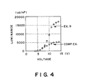
- Figure 4 is a graph showing voltage-luminescence characteristics of organic luminescence device of Example 9 and Comparative Example.
- organic boron compound of the present invention is represented by formula (1) below:
- Ar 1 denotes an optionally substituted aryl group or heterocyclic group.
- aryl group may include: monocyclic groups, such as phenyl, tolyl, aminophenyl, nitrophenyl, and halogenated phenyl; and polycyclic aromatic group, such as biphenyl, terphenyl, naphthyl, and anthranyl.
- heterocyclic group may include: monocyclic heterocyclic groups, inclusive of pyridyl, and 5-membered ring groups, such as pyrrolyl, thienyl, imidazolyl and pyrazolyl; and condensed heterocyclic group inclusive of 6,6-condensed heterocyclic groups, such as quinolyl and acridinyl, and 6,5-condensed heterocyclic groups, such as indolinyl.
- substituents optionally possessed by the aryl or heterocyclic group may include: halogen, alkyl, alkoxy, amino, imino, acetyl, formyl, nitro, silyl, aryl, heterocyclic group, and nitrile.
- the halogen substituents may include chloro, bromo, fluoro and iodo;
- the alkyl substituents may include linear alkyls such as methyl, ethyl and propyl; branched alkyls such as isobutyl and isopropyl, and substituted alkyls inclusive of aralkyl, such as benzyl;
- the aminoalkoxy substituents may include methoxy and ethoxy;
- the amino substituents may include secondary amino groups and ternary amino groups;
- the silyl substituents may includes dimethylsilyl, diphenylsilyl and t-butyldiphenylsilyl;
- the aryl substituents may include optionally substituted monocyclic groups such as phenyl, and optionally substituted polycyclic aromatic group such as biphenyl, terphenyl, naphthyl and anthranyl.
- the heterocyclic group substituents may include monocyclic heterocyclic groups such as quinolyl, pyrrolyl and thienyl, and condensed heterocyclic groups inclusive of 6,6-condensed heterocyclic groups such as acridinyl, and 6,5-condensed heterocyclic groups such as indolinyl.
- the substituents R 1 - R 11 independently denote hydrogen, halogen alkyl, alkenyl, amino, alkoxy, formyl, nitrile, aroyl, alkyloyl, aryl, aralkyl or heterocyclic group, each optionally substituted with the proviso that an adjacent one or more pairs of R 1 - R 11 , i.e., a pair of R 1 and R 2 , R 2 and R 3 , R 3 and R 4 , R 4 and R 5 , R 5 and R 6 , R 6 and R 7 , R 8 and R 9 , R 9 and R 10 , R 10 and R 11 , or R 11 and R 1 , can form a condensed ring.
- halogen examples include: chloro, bromo, fluoro and iodo.
- alkyl may include linear or branched alkyl groups having 1 to 20 carbon atoms, inclusive of linear alkyl groups, such as methyl, ethyl, n-propyl, n-octyl and n-decyl; and branched alkyl groups, such as isopropyl and t-butyl.
- alkenyl examples include: vinyl.
- Examples of the amino may include: non-substituted amino; mono-substituted amino groups substituted with one alkyl, aralkyl or aryl; and disubstituted amino groups substituted with two of alkyl, aralkyl and aryl groups.
- Examples of the substituent alkyl groups may include: linear alkyls, such as methyl, ethyl, n-propyl, n-octyl and n-decyl; and branched alkyls, such as isopropyl and t-butyl.
- alkoxy may include: alkyloxy groups and aromatic oxy groups, such as methoxy, ethoxy and phenyloxy.
- Examples of the aroyl may include: benzoyl, naphthoyl and anthroyl.
- alkyloyl may include: linear or branched aliphatic carbonyl groups, such as acetyl, n-propionyl, and isobutyroyl; and cyclic aliphatic carbonyl groups, such as cyclohexylcarbonyl.
- aryl may include: monocyclic aromatic groups and aromatic condensed ring groups, such as phenyl, naphthyl and anthranyl.
- Examples of the aralkyl may include: benzyl, pyridylmethyl and naphthomethyl.
- heterocyclic group may include: monocyclic heterocyclic groups, such as furyl, thienyl, pyrrolyl, imidazolyl and pyridyl; and condensed heterocyclic groups, such as indolyl, and amidinyl.
- substituents can be further substituted.
- substituents may include: halogen, alkyl, amino, alkoxy, formyl, nitrile, nitro, aroyl, alkyloyl, optionally substituted aryl, optionally substituted aralkyl, and optionally substituted heterocyclic group, wherein the substituents for the optionally substituted aryl, aralkyl and heterocyclic group may include: halogen, allyl, amino, alkoxy, formyl, nitrile, aroyl, alkylonyl, optionally substituted aryl, optionally substituted aralkyl and optionally substituted heterocyclic groups, but these are to exhaustive. Specific examples thereof may include those enumerated above.
- examples of the condensed ring which can be formed by a combination of the above-mentioned adjacent one or more pairs of R 1 - R 11 may include: single-ring structures and condensed ring structures, such as benzo, anthro, pyrido, pyrazino, imidazo, thieno, pyrazolo, and carbazolo.
- organic boron compound represented by the formula (1) are enumerated below by way of structural formulae, but they are not exhaustive. In the following structural formulae, some symbols are used for representing substituent groups, e.g., Me for methyl, Ph for phenyl and t-Bu for tert-butyl.
- the above-mentioned organic boron compound of the formula (1) may be produced through a step of reacting an aromatic ketone compound, preferably a benzoyl ketone compound, with an aromatic ketone compound, preferably a benzoyl ketone compound, or an aromatic aldehyde compound, preferably a benzaldehyde compound, in the presence of ammonium acetate, and a step of reacting the reaction product of the above step with an organic boric acid compound, preferably an aromatic boric acid compound.
- an aromatic ketone compound preferably a benzoyl ketone compound
- an aromatic ketone compound preferably a benzoyl ketone compound
- an aromatic aldehyde compound preferably a benzaldehyde compound
- the organic boron compound of the formula (1) may be synthesized by subjecting a ketone compound X and a ketone compound Y to a ring-addition reaction together with ammonium acetate to form a pyridine compound and reacting the pyridine compound with a boric acid compound to cause an addition reaction.
- the pyridine compound of the formula (4) above can also be synthesized through the following steps.
- the compound of the formula (7) is hydrolyzed under an acidic condition to form a compound of formula (8) below (which can also be represented by the above formula (4)): (wherein R 21 - R 29 are identified above).
- the compound of the formula (10) or (11) is substantially identical to the one represented by the formula (1).
- the compound of formula (2) and the compound of formula (3) may preferably be reacted in a mol ratio of 2:5 to 5:2.
- the ammonium acetate may preferably be used in an amount of at least 10 times the compound of formula (2) in terms of a mol ratio.
- the reaction may preferably be effected in a solvent, such as acetic acid, at 70 - 100 °C for 3 - 20 hours.
- the compound of formula (5) and the compound of formula (6) may preferably be reacted in a mol ratio of 1:1 to 4:1.
- the ammonium acetate may preferably be used in an amount of at least 10 times the compound of formula (5) in terms of a mol ratio.
- the reaction may preferably be effected in a solvent, such as acetic acid, at 70 - 100 °C for 3 - 20 hours.
- the hydrolysis of the compound of formula (7) may preferably be effected by using an acid, such as hydrobromic acid at 70 - 100 °C for 3 - 10 hours.
- the compound of formula (4) or (8) and the compound of formula (9) may preferably be reacted in a mol ratio of 1:1 to 1:4.
- the reaction may preferably be effected in a solvent, such as acetic acid at 20 - 100 °C for 1 - 10 hours.
- the organic boron compound of the present invention exhibits a strong fluorescence emission characteristic and accordingly is suitably used not only in an organic luminescence device as described below but also useful, e.g., as a reagent for quantitative analysis of boric acid, etc.
- an organic luminescence device comprising a pair of electrodes and a layer comprising the organic boron compound of the formula
- the organic compound layer comprising the above-mentioned organic boron compound of the formula (1) may be formed between the pair of anode and cathode (electrodes) by vacuum deposition or wet-coating process.
- the organic compound layer may preferably be formed in a thickness of at most 10 ⁇ m, more preferably at most 0.5 ⁇ m, further preferably 0.01 - 0.5 ⁇ m.
- a luminescence device of the present invention by disposing between a pair of electrodes a plurality of layers including at least one layer comprising the above-mentioned, organic boron compound of the formula (1). According to the present invention, by appropriately selecting an organic boron compound from a range of compounds represented by the formula (1), it is possible to provide a luminescence device emitting a desired color of luminescence.
- the organic compound layer constituting the organic luminescence device of the present invention may have a single-layer structure as shown in Figure 1 or a laminate structure of two or more layers as shown in Figures 2 and 3.
- Figure 1 is a schematic sectional view illustrating an embodiment of the organic luminescence device of the present invention.
- the organic luminescence device includes a substrate 1, and an anode 2, a luminescence layer 3 and a cathode disposed in this order on the substrate 1 so as to form a laminate structure.
- the luminescence layer 3 may comprise a single species of luminescent material exhibiting a hole-transporting function, an electron-transporting function and a luminescence function in combination or a mixture of plural compounds exhibiting these functions, respectively.
- the luminescence layer 3 may have a thickness of 5 nm to 1 ⁇ m, preferably 10 - 500 nm.
- Figure 2 is a sectional view showing a laminate structure of another embodiment of the organic luminescence device.
- the organic luminescence device includes a substrate 1, and an anode 2, a hole-transporting layer 5, an electron-transporting layer 6 and a cathode 4 disposed successively in this order on the substrate 1 so as to form a laminate structure, either one or both of the hole-transporting layer 5 and the electron-transporting layer 6 may contain a luminescent material also having a hole-transporting function and/or an electron-transporting function, respectively, for constituting a luminescence layer 3 in combination.
- One of the layers 6 and 5 may contain a material having no luminescent function but having a good electron-transporting or hole-transporting function.
- Each of the hole-transporting layer 5 and the electron-transporting layer 6 may have a thickness of 5 nm to 1 ⁇ m, preferably 10 - 500 nm.
- FIG. 3 is a sectional view showing still another embodiment of the organic luminescence device of the present invention.
- the organic luminescence device includes a substrate 1, and an anode 2, a hole-transporting layer 5, a luminescence layer 3, an electron-transporting layer 6 and a cathode 4 disposed successively in this order on the substrate 1 to form a laminate structure.
- the carrier transporting functions and the luminescent function of the organic compound layer are separated and assigned to the respective layers.
- Each of the hole-transporting layer 5, the luminescence layer 3 and the electron-transporting layer 6 may contain a single species or plural species of compounds showing respectively expected functions so as to exhibit desired performances. More specifically, in the case of using plural species of compounds in combination, a lot of latitude is provided in selection of materials for each layer, and various compounds having different emission wavelengths can be used to provide a variety of luminescence hues.
- each of the hole-transporting layer 5, the luminescence layer 3 and the electron-transporting layer 6 may have a thickness of 5 nm - 1 ⁇ m, preferably 10 - 500 nm.
- Figures 1 - 3 described above merely show basic structures of the organic luminescence device according to the present invention, and various modifications thereof are possible.
- an electron injection layer on the cathode side
- a hole injection layer on the anode side
- an insulating layer on the anode side
- an adhesive layer on the adhesive layer
- an interference layer on the hole-transporting layer 5
- the hole-transporting layer 5 can be divided into two layers with different ionization potentials.
- the layer comprising the organic boron compound of the formula (1) can be used to constitute any of the hole-injecting and transporting layer, the electron-transporting layer and the luminescence layer.
- the organic boron compound of the formula (1) can also be used to constitute such a functional layer, as desired in combination with a known hole-transporting compound, electron-transporting compound or luminescent compound, examples of which are enumerated hereinbelow.
- the organic compound layer containing the organic boron compound of the formula (1) or other organic compound layers may be formed into film by vacuum deposition or coating of a solution of the relevant compound in an appropriate solvent.
- the organic compound can be used in mixture with an appropriate binder resin to form a film.
- the organic compound, inclusive of the organic boron compound of the formula (1) may for example be used in 0.01 - 20 wt. parts, preferably, 0.1 - 10 wt. parts, per 1 wt. part of the binder resin.
- the binder resin used for the above purpose may be selected from a wide variety of scope. Examples thereof may include: polyvinyl carbazole resin, polycarbonate resin, polyester resin, polyarylate resin, polystyrene resin, acrylic resin, methacrylic resin, butyral resin, polyvinyl acetal resin, diallyl phthalate resin, phenolic resin, epoxy resin, silicone resin, polysulfone resin, and urea resin. These resins may be used singly or in combination of two or more species or in the form of copolymers.
- the anode As a material for the anode (2 shown in Figures 1 - 3), it is preferred to use one having as large a work function as possible, examples of which may include: metals, such as gold, platinum, nickel, palladium, cobalt, selenium and vanadium, and their alloys; metal oxides, such as tin oxide, zinc oxide, indium tin oxide (ITO), and indium zinc oxide; and electroconductive polymers, such as polyaniline, polypyrrole, polythiophene, and polyphenylene sulfide. These compounds may be used singly or in combination of two or more species.
- metals such as gold, platinum, nickel, palladium, cobalt, selenium and vanadium, and their alloys
- metal oxides such as tin oxide, zinc oxide, indium tin oxide (ITO), and indium zinc oxide
- electroconductive polymers such as polyaniline, polypyrrole, polythiophene, and polyphenylene sulfide.
- the cathode 4 shown in Figures 1 - 3 it is preferred to use one having a small work function, examples of which may include: metals, such as lithium, sodium, potassium, calcium, magnesium, aluminum, indium, silver, lead, tin and chromium, and their alloys. It is also possible to use metal oxide, such as indium tin oxide (ITO).
- ITO indium tin oxide
- the cathode may be formed in a single layer or a lamination of plural layers.
- the substrate 1 shown in Figures 1 - 3 for the organic luminescence device of the present invention may include an opaque substrate of metal, ceramics, etc., and a transparent substrate of glass, quartz, plastics, etc. It is possible to form the substrate with a color filter film, a fluorescent color conversion film, a dielectric reflection film, etc., thus controlling emitted luminescent light.
- the organic luminescence device of the present invention may further include a protective layer or a sealing layer.
- the protective layer may include: an inorganic film of diamond, metal oxide, metal nitride, etc.; a polymer film of fluorine-containing resin, polyparaxylene, polyethylene, silicone resin, polystyrene, etc., and a film of light-curable resin. It is also possible to effect packaging of the organic luminescence device per se with a sealing resin while covering the organic luminescence device with glass, gas-impermeable film, metal, etc.
- the reaction scheme is represented as follows.
- a 1.1 mm-thick glass substrate coated with a 120 nm-thick film of ITO (indium tin oxide) formed by sputtering was successively washed with acetone and isopropyl alcohol (IPA) under application of ultrasonic wave and then washed with IPA under boiling, followed by cleaning by UV/ozone (i.e., irradiation with ultraviolet rays in the ozone-containing atmosphere), to obtain a transparent conductive substrate (including a substrate 1 and an ITO anode 2 formed thereon).
- ITO indium tin oxide
- the transparent conductive substrate was coated by vacuum deposition first with N,N-diphenyl-N,N'-m-tolyl-4,4'-diamino-1,1'-biphenyl (hereinafter called "TPD") (hole-transporting material) in a thickness of 500 ⁇ (layer 5), then the above-listed Compound No. 2 in a thickness of 500 ⁇ (layer 6) and then Al in a thickness of 1500 ⁇ (cathode 4) to prepare a luminescence device.
- TPD N,N-diphenyl-N,N'-m-tolyl-4,4'-diamino-1,1'-biphenyl
- the device caused luminescence of green at luminances of 150 cd/m 2 at 9 volts.
- An ITO-coated transparent conductive substrate identical to the one used in Example 4 was first coated by vacuum deposition first with TPD in a thickness of 500 ⁇ (layer 5), then with Compound No. 16 in a thickness of 500 ⁇ (layer 6) and then with Al in a thickness of 1500 ⁇ (cathode 4) to prepare an organic luminescence device.
- the device caused luminescence of green at luminances of 200 cd/m 2 at 5 volts and 1500 cd/m 2 at 9 volts.
- An ITO-coated transparent conductive substrate identical to the one used in Example 4 was coated first by vacuum deposition with TPD in a thickness of 500 ⁇ , then by co-vavcuum deposition with Compound No. 16 and 1 % thereof of coumarin 6 (as dopant) in a thickness of 300 ⁇ , further by vacuum deposition with Compound No. 16 in a thickness of 200 ⁇ and then by vacuum deposition with Al in a thickness of 1500 ⁇ (cathode) to prepare an organic luminescence device.
- the device caused luminescence of green at luminances of 240 cd/m 2 at 5 volts and 300 cd/m 2 at 9 volts. As is understood from comparison with Example 5, the luminance at 9 volts was remarkably increased by adding coumarin 6 as a dopant.
- An ITO-coated transparent conductive substrate was coated by vacuum deposition first with TPD in a thickness of 500 ⁇ , then with Compound No. 17 in a thickness of 500 ⁇ and then with Al in a thickness of 1500 ⁇ (cathode) to prepare an organic luminescence device.
- the device caused luminescence of yellow at luminances of 40 cd/m 2 at 5 volts and 500 cd/m 2 at 9 volts.
- An ITO-coated transparent conductive substrate was coated by vacuum deposition first with TPD in a thickness of 500 ⁇ , then with Compound No. 17 in a thickness of 500 ⁇ , then with Al-Li alloy (Li content: 1 atom %) in a thickness of 100 ⁇ (as an electron-injecting layer) and then with Al in a thickness of 1500 ⁇ (cathode) to prepare an organic luminescence device.
- the device caused luminescence of green at luminances of 40 cd/m 2 at 5 volts and 500 cd/m at 9 volts.
- An ITO-coated transparent conductive substrate was coated by vacuum deposition first with TPD in a thickness of 500 ⁇ (layer 5), then with tris(8-quinolinolato)aluminum complex in a thickness of 500 ⁇ (luminescence layer 3 in Figure 3), then with Compound No. 17 in a thickness of 20 ⁇ (electron-injecting layer 6) and then with Al in a thickness of 1500 ⁇ (cathode 4) to prepare an organic luminescence device.
- An ITO-coated transparent conductive substrate was coated by vacuum deposition first with TPD in a thickness of 500 ⁇ (layer 5), tris(8-quinolinolato) aluminum complex in a thickness of 500 ⁇ (luminescence layer 3 or electron-injecting layer 6) and then with Al in a thickness of 1500 ⁇ (cathode 4) to provide an organic luminescence device.
- Example 9 and Comparative Example prepared above both caused luminescence of green and exhibited voltage-luminance characteristics shown in Figure 4, which show that Compound No. 17 (as an example of the organic boron compound of the present invention) provided a very effective electron-injecting layer.
- an organic boron compound of the formula (1) which is useful as a luminescence device material, particularly excellent in charge-transporting characteristics and useful for constituting a luminescence layer and/or an electron-transporting layer exhibiting excellent performances.
- the above organic boron compound can be produced easily and relatively inexpensively by the process for production thereof according to the present invention.
- the organic luminescence device of the present invention including a layer of the organic boron compound can exhibit luminescence of very high luminance at a low application voltage and thus exhibits excellent durability.
- An organic layer comprising the organic boron compound of the present invention is useful as an electron-transporting layer and a luminescence layer and is also useful as an electron-injecting layer.
- the layer can be easily formed by vacuum deposition or casting and therefore allows easy and inexpensive production of a large area device.
- An organic boron compound effective for constituting a functional layer in an organic luminescence device is represented by formula (1) below: wherein Ar 1 denotes an optionally substituted aryl group or heterocyclic group; R 1 - R 11 independently denote hydrogen, halogen, alkyl, alkenyl, amino, alkoxy, formyl, nitrile, aroyl, alkyloyl, aryl, aralkyl or heterocyclic group, each optionally substituted with the proviso that an adjacent one or more pairs of R 1 - R 11 can form a condensed ring.
- Ar 1 denotes an optionally substituted aryl group or heterocyclic group
- R 1 - R 11 independently denote hydrogen, halogen, alkyl, alkenyl, amino, alkoxy, formyl, nitrile, aroyl, alkyloyl, aryl, aralkyl or heterocyclic group, each optionally substituted with the proviso that an adjacent one or
- the organic boron compound can be produced through a process including (A) a step of reacting an aromatic ketone compound X with an aromatic ketone compound or an aromatic aldehyde compound in the presence of ammonium chloride, and (B) a step of reacting a product of the step (A) with an aromatic boric acid compound.
Landscapes
- Chemical & Material Sciences (AREA)
- Organic Chemistry (AREA)
- Electroluminescent Light Sources (AREA)
Applications Claiming Priority (2)
| Application Number | Priority Date | Filing Date | Title |
|---|---|---|---|
| JP2000096322 | 2000-03-31 | ||
| JP2000096322 | 2000-03-31 |
Publications (3)
| Publication Number | Publication Date |
|---|---|
| EP1138683A2 true EP1138683A2 (fr) | 2001-10-04 |
| EP1138683A3 EP1138683A3 (fr) | 2003-04-16 |
| EP1138683B1 EP1138683B1 (fr) | 2005-11-09 |
Family
ID=18611106
Family Applications (1)
| Application Number | Title | Priority Date | Filing Date |
|---|---|---|---|
| EP01108056A Expired - Lifetime EP1138683B1 (fr) | 2000-03-31 | 2001-03-29 | Dispositif organique luminescent contenant des nouveaux composés du bore et procédé pour préparer les composés |
Country Status (3)
| Country | Link |
|---|---|
| US (1) | US6461749B2 (fr) |
| EP (1) | EP1138683B1 (fr) |
| DE (1) | DE60114686T2 (fr) |
Cited By (3)
| Publication number | Priority date | Publication date | Assignee | Title |
|---|---|---|---|---|
| US7033681B2 (en) | 2004-03-18 | 2006-04-25 | Eastman Kodak Company | Organic element for electroluminescent devices |
| CN103649268A (zh) * | 2011-08-19 | 2014-03-19 | 第一毛织株式会社 | 用于有机光电子装置的化合物、包括该化合物的有机发光元件和包括该有机发光二极管的显示装置 |
| CN110446770A (zh) * | 2017-04-07 | 2019-11-12 | 百乐墨水株式会社 | 可逆热变色性组合物及内包有该组合物的可逆热变色性微胶囊颜料 |
Families Citing this family (1)
| Publication number | Priority date | Publication date | Assignee | Title |
|---|---|---|---|---|
| MY136312A (en) * | 2003-05-21 | 2008-09-30 | Ciba Holding Inc | Borate ester lubricant additives |
Family Cites Families (26)
| Publication number | Priority date | Publication date | Assignee | Title |
|---|---|---|---|---|
| US4539507A (en) | 1983-03-25 | 1985-09-03 | Eastman Kodak Company | Organic electroluminescent devices having improved power conversion efficiencies |
| US4885211A (en) | 1987-02-11 | 1989-12-05 | Eastman Kodak Company | Electroluminescent device with improved cathode |
| US4720432A (en) | 1987-02-11 | 1988-01-19 | Eastman Kodak Company | Electroluminescent device with organic luminescent medium |
| JP2922212B2 (ja) | 1989-02-17 | 1999-07-19 | パイオニア株式会社 | 電界発光素子 |
| JPH07119407B2 (ja) | 1989-03-20 | 1995-12-20 | 出光興産株式会社 | エレクトロルミネッセンス素子 |
| US5130603A (en) | 1989-03-20 | 1992-07-14 | Idemitsu Kosan Co., Ltd. | Organic electroluminescence device |
| GB8909011D0 (en) | 1989-04-20 | 1989-06-07 | Friend Richard H | Electroluminescent devices |
| JP2815472B2 (ja) | 1990-01-22 | 1998-10-27 | パイオニア株式会社 | 電界発光素子 |
| JP2998187B2 (ja) | 1990-10-04 | 2000-01-11 | 住友化学工業株式会社 | 有機エレクトロルミネッセンス素子 |
| DE69110922T2 (de) | 1990-02-23 | 1995-12-07 | Sumitomo Chemical Co | Organisch elektrolumineszente Vorrichtung. |
| GB9018698D0 (en) | 1990-08-24 | 1990-10-10 | Lynxvale Ltd | Semiconductive copolymers for use in electroluminescent devices |
| JP2721441B2 (ja) | 1991-02-27 | 1998-03-04 | 株式会社リコー | 電界発光素子 |
| US5382477A (en) | 1991-02-27 | 1995-01-17 | Sanyo Electric Co., Ltd. | Organic electroluminescent element and process for producing the same |
| US5151629A (en) | 1991-08-01 | 1992-09-29 | Eastman Kodak Company | Blue emitting internal junction organic electroluminescent device (I) |
| JPH05202356A (ja) | 1991-09-11 | 1993-08-10 | Pioneer Electron Corp | 有機エレクトロルミネッセンス素子 |
| JP3255190B2 (ja) | 1991-12-03 | 2002-02-12 | 日本電気株式会社 | 音声符号化装置並びにその分析器及び合成器 |
| JP3328731B2 (ja) | 1991-12-05 | 2002-09-30 | 住友化学工業株式会社 | 有機エレクトロルミネッセンス素子 |
| JP2734341B2 (ja) | 1993-03-26 | 1998-03-30 | 住友電気工業株式会社 | 有機エレクトロルミネッセンス素子 |
| EP0647694B1 (fr) | 1993-03-26 | 1999-09-15 | Sumitomo Electric Industries, Ltd. | Elements organiques electroluminescents |
| US5514878A (en) | 1994-03-18 | 1996-05-07 | Holmes; Andrew B. | Polymers for electroluminescent devices |
| JP2937015B2 (ja) | 1993-07-28 | 1999-08-23 | 住友電気工業株式会社 | 有機エレクトロルミネッセンス素子 |
| US5409783A (en) | 1994-02-24 | 1995-04-25 | Eastman Kodak Company | Red-emitting organic electroluminescent device |
| JPH09202878A (ja) | 1996-01-25 | 1997-08-05 | Nippon Telegr & Teleph Corp <Ntt> | 近紫外・紫外波長帯発光素子 |
| JPH09227576A (ja) | 1996-02-23 | 1997-09-02 | Sony Corp | 金属複核錯体、その製造方法及び光学的素子 |
| JPH09289081A (ja) * | 1996-04-23 | 1997-11-04 | Mitsubishi Chem Corp | 有機電界発光素子 |
| CN1107098C (zh) * | 1999-09-05 | 2003-04-30 | 吉林大学 | 酚基-吡啶或其衍生物的金属配合物和它们作为电致发光材料的应用 |
-
2001
- 2001-03-28 US US09/818,661 patent/US6461749B2/en not_active Expired - Fee Related
- 2001-03-29 DE DE60114686T patent/DE60114686T2/de not_active Expired - Lifetime
- 2001-03-29 EP EP01108056A patent/EP1138683B1/fr not_active Expired - Lifetime
Non-Patent Citations (1)
| Title |
|---|
| None |
Cited By (4)
| Publication number | Priority date | Publication date | Assignee | Title |
|---|---|---|---|---|
| US7033681B2 (en) | 2004-03-18 | 2006-04-25 | Eastman Kodak Company | Organic element for electroluminescent devices |
| CN103649268A (zh) * | 2011-08-19 | 2014-03-19 | 第一毛织株式会社 | 用于有机光电子装置的化合物、包括该化合物的有机发光元件和包括该有机发光二极管的显示装置 |
| CN110446770A (zh) * | 2017-04-07 | 2019-11-12 | 百乐墨水株式会社 | 可逆热变色性组合物及内包有该组合物的可逆热变色性微胶囊颜料 |
| CN110446770B (zh) * | 2017-04-07 | 2023-08-08 | 百乐墨水株式会社 | 可逆热变色性组合物及内包有该组合物的可逆热变色性微胶囊颜料 |
Also Published As
| Publication number | Publication date |
|---|---|
| EP1138683B1 (fr) | 2005-11-09 |
| EP1138683A3 (fr) | 2003-04-16 |
| DE60114686T2 (de) | 2006-08-03 |
| DE60114686D1 (de) | 2005-12-15 |
| US20020008465A1 (en) | 2002-01-24 |
| US6461749B2 (en) | 2002-10-08 |
Similar Documents
| Publication | Publication Date | Title |
|---|---|---|
| US11393989B2 (en) | Organic electroluminescent devices and metal complex compounds | |
| US6838194B2 (en) | Efficient organic electroluminescent devices with red fluorescent dopants | |
| JP4261855B2 (ja) | フェナントロリン化合物及びそれを用いた有機発光素子 | |
| EP1099744B1 (fr) | Dispositif organique électroluminescent | |
| KR100761621B1 (ko) | 플루오렌화합물 및 이것을 이용한 유기발광소자 | |
| US7101632B2 (en) | Cyclocondensed polycyclic hydrocarbon compound and light-emitting device using the same | |
| US7691492B2 (en) | Fluorene compound and organic light-emitting device using same | |
| US7923129B2 (en) | Carbazole derivative and organic light emitting device using the same | |
| JP4585750B2 (ja) | 縮合多環化合物及びそれを用いた有機発光素子 | |
| KR101188461B1 (ko) | 축합환 방향족 화합물 및 이것을 이용한 유기 발광소자 | |
| EP2132157B1 (fr) | Nouveau compose aromatique a cycle condense, et dispositif electroluminescent organique le comprenant | |
| US20020177009A1 (en) | Fused polynuclear compound and organic luminescence device | |
| EP0757088A2 (fr) | Elément électroluminescent organique et dispositif émettant de la lumière utilisant cet élément | |
| US7749617B2 (en) | Organic compound and organic light-emitting device | |
| JP4224252B2 (ja) | 有機el素子用化合物、有機el素子 | |
| US20090001880A1 (en) | Organic electroluminescent device, an azepine compound, and a method for making the same | |
| JP3475620B2 (ja) | 有機エレクトロルミネッセンス素子材料およびそれを使用した有機エレクトロルミネッセンス素子 | |
| JP2003109763A (ja) | 有機発光素子 | |
| EP1138683B1 (fr) | Dispositif organique luminescent contenant des nouveaux composés du bore et procédé pour préparer les composés | |
| US6649089B2 (en) | Red organic electroluminescent materials | |
| JP3990869B2 (ja) | 有機ほう素化合物、該有機ほう素化合物の製造方法、及び該有機ほう素化合物を用いた有機発光素子 | |
| KR100492243B1 (ko) | 새로운 유기붕소화합물을 사용하는 유기발광소자 및 해당 소자의 제조방법 | |
| JP4256556B2 (ja) | 発光素子材料、それを使用した発光素子およびアミン化合物 | |
| JP2003077671A (ja) | 有機発光素子 | |
| JP3741341B2 (ja) | 有機発光素子材料およびそれを使用した有機発光素子 |
Legal Events
| Date | Code | Title | Description |
|---|---|---|---|
| PUAI | Public reference made under article 153(3) epc to a published international application that has entered the european phase |
Free format text: ORIGINAL CODE: 0009012 |
|
| 17P | Request for examination filed |
Effective date: 20010329 |
|
| AK | Designated contracting states |
Kind code of ref document: A2 Designated state(s): AT BE CH CY DE DK ES FI FR GB GR IE IT LI LU MC NL PT SE TR |
|
| AX | Request for extension of the european patent |
Free format text: AL;LT;LV;MK;RO;SI |
|
| PUAL | Search report despatched |
Free format text: ORIGINAL CODE: 0009013 |
|
| AK | Designated contracting states |
Designated state(s): AT BE CH CY DE DK ES FI FR GB GR IE IT LI LU MC NL PT SE TR |
|
| AX | Request for extension of the european patent |
Extension state: AL LT LV MK RO SI |
|
| 17Q | First examination report despatched |
Effective date: 20030617 |
|
| AKX | Designation fees paid |
Designated state(s): DE FI FR GB IT |
|
| GRAP | Despatch of communication of intention to grant a patent |
Free format text: ORIGINAL CODE: EPIDOSNIGR1 |
|
| RIC1 | Information provided on ipc code assigned before grant |
Ipc: 7H 01L 51/20 A Ipc: 7C 07F 5/02 B |
|
| RTI1 | Title (correction) |
Free format text: ORGANIC LUMINESCENCE DEVICE USING NOVEL ORGANIC BORON COMPOUNDS AND PROCESS FOR PRODUCING THE COMPOUNDS |
|
| RTI1 | Title (correction) |
Free format text: ORGANIC LUMINESCENCE DEVICE USING NOVEL ORGANIC BORON COMPOUNDS AND PROCESS FOR PRODUCING THESE COMPOUNDS |
|
| GRAS | Grant fee paid |
Free format text: ORIGINAL CODE: EPIDOSNIGR3 |
|
| GRAA | (expected) grant |
Free format text: ORIGINAL CODE: 0009210 |
|
| AK | Designated contracting states |
Kind code of ref document: B1 Designated state(s): DE FI FR GB IT |
|
| PG25 | Lapsed in a contracting state [announced via postgrant information from national office to epo] |
Ref country code: IT Free format text: LAPSE BECAUSE OF FAILURE TO SUBMIT A TRANSLATION OF THE DESCRIPTION OR TO PAY THE FEE WITHIN THE PRESCRIBED TIME-LIMIT;WARNING: LAPSES OF ITALIAN PATENTS WITH EFFECTIVE DATE BEFORE 2007 MAY HAVE OCCURRED AT ANY TIME BEFORE 2007. THE CORRECT EFFECTIVE DATE MAY BE DIFFERENT FROM THE ONE RECORDED. Effective date: 20051109 Ref country code: FI Free format text: LAPSE BECAUSE OF FAILURE TO SUBMIT A TRANSLATION OF THE DESCRIPTION OR TO PAY THE FEE WITHIN THE PRESCRIBED TIME-LIMIT Effective date: 20051109 |
|
| REG | Reference to a national code |
Ref country code: GB Ref legal event code: FG4D |
|
| REF | Corresponds to: |
Ref document number: 60114686 Country of ref document: DE Date of ref document: 20051215 Kind code of ref document: P |
|
| PG25 | Lapsed in a contracting state [announced via postgrant information from national office to epo] |
Ref country code: GB Free format text: LAPSE BECAUSE OF NON-PAYMENT OF DUE FEES Effective date: 20060329 |
|
| PLBE | No opposition filed within time limit |
Free format text: ORIGINAL CODE: 0009261 |
|
| STAA | Information on the status of an ep patent application or granted ep patent |
Free format text: STATUS: NO OPPOSITION FILED WITHIN TIME LIMIT |
|
| 26N | No opposition filed |
Effective date: 20060810 |
|
| PG25 | Lapsed in a contracting state [announced via postgrant information from national office to epo] |
Ref country code: FR Free format text: LAPSE BECAUSE OF FAILURE TO SUBMIT A TRANSLATION OF THE DESCRIPTION OR TO PAY THE FEE WITHIN THE PRESCRIBED TIME-LIMIT Effective date: 20061020 |
|
| GBPC | Gb: european patent ceased through non-payment of renewal fee |
Effective date: 20060329 |
|
| EN | Fr: translation not filed | ||
| PG25 | Lapsed in a contracting state [announced via postgrant information from national office to epo] |
Ref country code: FR Free format text: LAPSE BECAUSE OF FAILURE TO SUBMIT A TRANSLATION OF THE DESCRIPTION OR TO PAY THE FEE WITHIN THE PRESCRIBED TIME-LIMIT Effective date: 20051109 |
|
| PGFP | Annual fee paid to national office [announced via postgrant information from national office to epo] |
Ref country code: DE Payment date: 20140331 Year of fee payment: 14 |
|
| REG | Reference to a national code |
Ref country code: DE Ref legal event code: R119 Ref document number: 60114686 Country of ref document: DE |
|
| PG25 | Lapsed in a contracting state [announced via postgrant information from national office to epo] |
Ref country code: DE Free format text: LAPSE BECAUSE OF NON-PAYMENT OF DUE FEES Effective date: 20151001 |