EP1139323A2 - Dispositif d'affichage à plasma et méthode de fabrication - Google Patents
Dispositif d'affichage à plasma et méthode de fabrication Download PDFInfo
- Publication number
- EP1139323A2 EP1139323A2 EP00309848A EP00309848A EP1139323A2 EP 1139323 A2 EP1139323 A2 EP 1139323A2 EP 00309848 A EP00309848 A EP 00309848A EP 00309848 A EP00309848 A EP 00309848A EP 1139323 A2 EP1139323 A2 EP 1139323A2
- Authority
- EP
- European Patent Office
- Prior art keywords
- sustaining
- circuit
- electrodes
- electrode
- plasma display
- Prior art date
- Legal status (The legal status is an assumption and is not a legal conclusion. Google has not performed a legal analysis and makes no representation as to the accuracy of the status listed.)
- Withdrawn
Links
- 238000004519 manufacturing process Methods 0.000 title claims description 11
- 238000011084 recovery Methods 0.000 claims abstract description 31
- 239000003990 capacitor Substances 0.000 claims description 30
- 230000000630 rising effect Effects 0.000 claims 4
- 230000007257 malfunction Effects 0.000 abstract description 6
- 230000001976 improved effect Effects 0.000 abstract description 3
- 230000006866 deterioration Effects 0.000 abstract description 2
- 238000000034 method Methods 0.000 description 16
- 238000009966 trimming Methods 0.000 description 6
- 230000007423 decrease Effects 0.000 description 4
- 230000003247 decreasing effect Effects 0.000 description 4
- 238000010586 diagram Methods 0.000 description 4
- 230000000694 effects Effects 0.000 description 4
- 238000001514 detection method Methods 0.000 description 3
- 238000010276 construction Methods 0.000 description 2
- 230000003111 delayed effect Effects 0.000 description 2
- 238000005401 electroluminescence Methods 0.000 description 2
- 230000010363 phase shift Effects 0.000 description 2
- 230000002159 abnormal effect Effects 0.000 description 1
- 230000001934 delay Effects 0.000 description 1
- 238000011835 investigation Methods 0.000 description 1
- 230000010355 oscillation Effects 0.000 description 1
- 239000002699 waste material Substances 0.000 description 1
Images







Classifications
-
- G—PHYSICS
- G09—EDUCATION; CRYPTOGRAPHY; DISPLAY; ADVERTISING; SEALS
- G09G—ARRANGEMENTS OR CIRCUITS FOR CONTROL OF INDICATING DEVICES USING STATIC MEANS TO PRESENT VARIABLE INFORMATION
- G09G3/00—Control arrangements or circuits, of interest only in connection with visual indicators other than cathode-ray tubes
- G09G3/20—Control arrangements or circuits, of interest only in connection with visual indicators other than cathode-ray tubes for presentation of an assembly of a number of characters, e.g. a page, by composing the assembly by combination of individual elements arranged in a matrix no fixed position being assigned to or needed to be assigned to the individual characters or partial characters
- G09G3/22—Control arrangements or circuits, of interest only in connection with visual indicators other than cathode-ray tubes for presentation of an assembly of a number of characters, e.g. a page, by composing the assembly by combination of individual elements arranged in a matrix no fixed position being assigned to or needed to be assigned to the individual characters or partial characters using controlled light sources
- G09G3/28—Control arrangements or circuits, of interest only in connection with visual indicators other than cathode-ray tubes for presentation of an assembly of a number of characters, e.g. a page, by composing the assembly by combination of individual elements arranged in a matrix no fixed position being assigned to or needed to be assigned to the individual characters or partial characters using controlled light sources using luminous gas-discharge panels, e.g. plasma panels
- G09G3/288—Control arrangements or circuits, of interest only in connection with visual indicators other than cathode-ray tubes for presentation of an assembly of a number of characters, e.g. a page, by composing the assembly by combination of individual elements arranged in a matrix no fixed position being assigned to or needed to be assigned to the individual characters or partial characters using controlled light sources using luminous gas-discharge panels, e.g. plasma panels using AC panels
- G09G3/296—Driving circuits for producing the waveforms applied to the driving electrodes
-
- G—PHYSICS
- G09—EDUCATION; CRYPTOGRAPHY; DISPLAY; ADVERTISING; SEALS
- G09G—ARRANGEMENTS OR CIRCUITS FOR CONTROL OF INDICATING DEVICES USING STATIC MEANS TO PRESENT VARIABLE INFORMATION
- G09G3/00—Control arrangements or circuits, of interest only in connection with visual indicators other than cathode-ray tubes
- G09G3/20—Control arrangements or circuits, of interest only in connection with visual indicators other than cathode-ray tubes for presentation of an assembly of a number of characters, e.g. a page, by composing the assembly by combination of individual elements arranged in a matrix no fixed position being assigned to or needed to be assigned to the individual characters or partial characters
- G09G3/22—Control arrangements or circuits, of interest only in connection with visual indicators other than cathode-ray tubes for presentation of an assembly of a number of characters, e.g. a page, by composing the assembly by combination of individual elements arranged in a matrix no fixed position being assigned to or needed to be assigned to the individual characters or partial characters using controlled light sources
- G09G3/28—Control arrangements or circuits, of interest only in connection with visual indicators other than cathode-ray tubes for presentation of an assembly of a number of characters, e.g. a page, by composing the assembly by combination of individual elements arranged in a matrix no fixed position being assigned to or needed to be assigned to the individual characters or partial characters using controlled light sources using luminous gas-discharge panels, e.g. plasma panels
- G09G3/288—Control arrangements or circuits, of interest only in connection with visual indicators other than cathode-ray tubes for presentation of an assembly of a number of characters, e.g. a page, by composing the assembly by combination of individual elements arranged in a matrix no fixed position being assigned to or needed to be assigned to the individual characters or partial characters using controlled light sources using luminous gas-discharge panels, e.g. plasma panels using AC panels
- G09G3/296—Driving circuits for producing the waveforms applied to the driving electrodes
- G09G3/2965—Driving circuits for producing the waveforms applied to the driving electrodes using inductors for energy recovery
-
- G—PHYSICS
- G09—EDUCATION; CRYPTOGRAPHY; DISPLAY; ADVERTISING; SEALS
- G09G—ARRANGEMENTS OR CIRCUITS FOR CONTROL OF INDICATING DEVICES USING STATIC MEANS TO PRESENT VARIABLE INFORMATION
- G09G3/00—Control arrangements or circuits, of interest only in connection with visual indicators other than cathode-ray tubes
- G09G3/20—Control arrangements or circuits, of interest only in connection with visual indicators other than cathode-ray tubes for presentation of an assembly of a number of characters, e.g. a page, by composing the assembly by combination of individual elements arranged in a matrix no fixed position being assigned to or needed to be assigned to the individual characters or partial characters
- G09G3/22—Control arrangements or circuits, of interest only in connection with visual indicators other than cathode-ray tubes for presentation of an assembly of a number of characters, e.g. a page, by composing the assembly by combination of individual elements arranged in a matrix no fixed position being assigned to or needed to be assigned to the individual characters or partial characters using controlled light sources
- G09G3/28—Control arrangements or circuits, of interest only in connection with visual indicators other than cathode-ray tubes for presentation of an assembly of a number of characters, e.g. a page, by composing the assembly by combination of individual elements arranged in a matrix no fixed position being assigned to or needed to be assigned to the individual characters or partial characters using controlled light sources using luminous gas-discharge panels, e.g. plasma panels
- G09G3/288—Control arrangements or circuits, of interest only in connection with visual indicators other than cathode-ray tubes for presentation of an assembly of a number of characters, e.g. a page, by composing the assembly by combination of individual elements arranged in a matrix no fixed position being assigned to or needed to be assigned to the individual characters or partial characters using controlled light sources using luminous gas-discharge panels, e.g. plasma panels using AC panels
- G09G3/298—Control arrangements or circuits, of interest only in connection with visual indicators other than cathode-ray tubes for presentation of an assembly of a number of characters, e.g. a page, by composing the assembly by combination of individual elements arranged in a matrix no fixed position being assigned to or needed to be assigned to the individual characters or partial characters using controlled light sources using luminous gas-discharge panels, e.g. plasma panels using AC panels using surface discharge panels
- G09G3/299—Control arrangements or circuits, of interest only in connection with visual indicators other than cathode-ray tubes for presentation of an assembly of a number of characters, e.g. a page, by composing the assembly by combination of individual elements arranged in a matrix no fixed position being assigned to or needed to be assigned to the individual characters or partial characters using controlled light sources using luminous gas-discharge panels, e.g. plasma panels using AC panels using surface discharge panels using alternate lighting of surface-type panels
-
- G—PHYSICS
- G09—EDUCATION; CRYPTOGRAPHY; DISPLAY; ADVERTISING; SEALS
- G09G—ARRANGEMENTS OR CIRCUITS FOR CONTROL OF INDICATING DEVICES USING STATIC MEANS TO PRESENT VARIABLE INFORMATION
- G09G2330/00—Aspects of power supply; Aspects of display protection and defect management
- G09G2330/02—Details of power systems and of start or stop of display operation
- G09G2330/021—Power management, e.g. power saving
-
- G—PHYSICS
- G09—EDUCATION; CRYPTOGRAPHY; DISPLAY; ADVERTISING; SEALS
- G09G—ARRANGEMENTS OR CIRCUITS FOR CONTROL OF INDICATING DEVICES USING STATIC MEANS TO PRESENT VARIABLE INFORMATION
- G09G3/00—Control arrangements or circuits, of interest only in connection with visual indicators other than cathode-ray tubes
- G09G3/20—Control arrangements or circuits, of interest only in connection with visual indicators other than cathode-ray tubes for presentation of an assembly of a number of characters, e.g. a page, by composing the assembly by combination of individual elements arranged in a matrix no fixed position being assigned to or needed to be assigned to the individual characters or partial characters
- G09G3/22—Control arrangements or circuits, of interest only in connection with visual indicators other than cathode-ray tubes for presentation of an assembly of a number of characters, e.g. a page, by composing the assembly by combination of individual elements arranged in a matrix no fixed position being assigned to or needed to be assigned to the individual characters or partial characters using controlled light sources
- G09G3/28—Control arrangements or circuits, of interest only in connection with visual indicators other than cathode-ray tubes for presentation of an assembly of a number of characters, e.g. a page, by composing the assembly by combination of individual elements arranged in a matrix no fixed position being assigned to or needed to be assigned to the individual characters or partial characters using controlled light sources using luminous gas-discharge panels, e.g. plasma panels
- G09G3/288—Control arrangements or circuits, of interest only in connection with visual indicators other than cathode-ray tubes for presentation of an assembly of a number of characters, e.g. a page, by composing the assembly by combination of individual elements arranged in a matrix no fixed position being assigned to or needed to be assigned to the individual characters or partial characters using controlled light sources using luminous gas-discharge panels, e.g. plasma panels using AC panels
- G09G3/291—Control arrangements or circuits, of interest only in connection with visual indicators other than cathode-ray tubes for presentation of an assembly of a number of characters, e.g. a page, by composing the assembly by combination of individual elements arranged in a matrix no fixed position being assigned to or needed to be assigned to the individual characters or partial characters using controlled light sources using luminous gas-discharge panels, e.g. plasma panels using AC panels controlling the gas discharge to control a cell condition, e.g. by means of specific pulse shapes
- G09G3/294—Control arrangements or circuits, of interest only in connection with visual indicators other than cathode-ray tubes for presentation of an assembly of a number of characters, e.g. a page, by composing the assembly by combination of individual elements arranged in a matrix no fixed position being assigned to or needed to be assigned to the individual characters or partial characters using controlled light sources using luminous gas-discharge panels, e.g. plasma panels using AC panels controlling the gas discharge to control a cell condition, e.g. by means of specific pulse shapes for lighting or sustain discharge
Definitions
- the present invention relates to a plasma display apparatus and a method of manufacturing the same.
- the present invention relates to a plasma display apparatus equipped with a power recovery circuit in a sustaining circuit that reduces power consumption, a plasma display panel employing the ALIS (Alternate Lighting of Surfaces) system, in which plural first and second electrodes are arranged adjacently and display lines are formed between every pair of adjacent electrodes, and to control circuitry for a plasma display panel.
- ALIS Alternate Lighting of Surfaces
- the plasma display panel has good visibility because it generates its own light, is thin and can be made with a large and high-speed display, therefore, it is attracting interest as a replacement for the CRT display. Since the structure of a typical PDP has been disclosed in Japanese Unexamined Patent Publication (Kokai) No. 7-160219, Japanese Unexamined Patent Publication (Kokai) No. 9-160525, and Japanese Unexamined Patent Publication (Kokai) No. 9-325735, a detailed explanation is omitted here and, instead, only points relating directly to the present invention are explained.
- FIG.1 is a block diagram showing the overall structure of a general PDP apparatus.
- n X electrodes 11 and Y electrodes 12 are arranged adjacently by turns, forming n pairs each of one X and one Y electrode 12, and light is emitted for display between the X electrode 11 and Y electrode 12 of each pair.
- Y electrodes and X electrodes are called display electrodes or sustaining electrodes.
- Address electrodes 13 which are normal to the display electrodes are provided, and display cells are formed at crossings of the address electrodes and X-Y electrode pairs.
- the Y electrodes 12 are connected to a scan driver 14 (see Figure 2); this is equipped with switches 16, the number of which being equal to that of the Y electrodes and the switches are switched so that scan pulses from a scan signal generating circuit 15 are applied sequentially during the address period, and sustaining pulses from a Y sustaining circuit 19 are applied simultaneously during the sustaining discharge period.
- the X electrodes 11 are connected commonly to an X sustaining circuit 18, and the address electrodes 13 are connected to an address driver circuit 17.
- image signals are converted so as suit the operation in the PDP apparatus, and are then supplied to the address driver circuit 17.
- a drive control circuit 20 generates and supplies signals that control each part of the PDP apparatus.
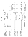
- FIG.2 is a time chart showing drive signals of the PDP apparatus.
- a display frame is refreshed at predetermined intervals, and a display period is called a field.
- a field is divided into a plurality of subfields and the subfields that emit light are selected for each display cell.
- Each subfield consists of the reset period during which all display cells are initialized, the address period during which all display cells are put into the status corresponding to the display image, and the sustaining discharge period during which each display cell emits light according to the set status.
- sustaining pulses are applied to X electrodes and Y electrodes alternately and sustaining discharges are performed in the display cell specified to emit light during the address period, resulting in light emission for display.
- FIG.3 is a schematic showing an example of a typical construction of a sustaining circuit equipped with a power recovery circuit, in which a circuit to recover power (i.e. electrical charge) and a circuit to apply the accumulated power is separated. Circuits to-generate signals V1 to V4 are also provided, but they are omitted here.
- Reference code Cp refers to a drive capacitance of a display cell, formed by the X electrode and Y electrode of a PDP. Though a sustaining circuit of one of the electrodes is shown here, the other electrode is also connected to a similar sustaining circuit.
- the part consisting of output devices (transistors) 31 and 33, and drive circuits 32 and 34 is a sustaining circuit without a power recovery circuit
- the part consisting of output devices (transistors) 37 and 40, drive circuits 38 and 41, inductance devices 35 and 43, capacitor 39, and diodes 36 and 42 is a power recovery circuit.
- the signals V1 and V2 are supplied to the drive circuits 32 and 34, respectively, and the signals VG1 and VG2 output therefrom are supplied to the gates of the output devices (transistors) 31 and 33.
- the signal V1 is "High (H)"
- the output device 31 turns on and an H level signal is applied to the electrode.
- the signal V2 is "Low (L)", and the output device 33 is off.
- the signal V1 turns to L and the output device 31 turns off, the signal V2 turns to H and the output device 33 turns on, and the ground level is applied to the electrode.
- the signal V1 turns to L first and after the output device 31 turns off, the signal V4 turns to H, the output device 37 turns on, and a resonant circuit is formed by the capacitor 39, diode 36, inductor 35, and capacitor Cp, and the charge stored in the capacitor Cp is supplied to the capacitor 39, thus the voltage of the capacitor 39 is raised. Therefore, the charge stored in the capacitor Cp is transferred to the capacitor 39 by the sustaining pulses applied to the electrode.
- the signal V4 turns to L, the output device 37 turns off, then the signal V2 turns to H, the output device 33 turns on, and the potential of the electrode is fixed at ground level.
- the above-mentioned operation is repeated a number of times equal to that of the sustaining pulses. In the structure mentioned above, the power consumption caused by the sustaining discharge can be suppressed.
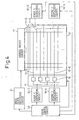
- FIG.4 is a general block diagram of a PDP employing the ALIS system.
- n Y electrodes (second electrodes) 12 - O and 12 - E and n+1 X electrodes (first electrodes) 11 - O and 11 - E are arranged adjacently in turn and light is emitted between every adjacent display electrode (Y electrode and X electrode). Therefore, 2n+1 display electrodes form 2n display lines. This means that the precision can be doubled with the same number of the display electrodes as that in FIG.1, in the ALIS system.
- the ALIS system is also characterized by a high luminance because the discharge space can be used efficiently without any waste and a high opening ratio can be obtained to give a small loss of light due to electrodes or the like.
- Light is emitted between every adjacent display electrode for display in the ALIS system, but it is impossible to cause all discharges to occur at the same time. Therefore, so-called interlaced scanning, in which odd-numbered lines and even-numbered lines are used in a time-shared manner for display, is employed. In the odd field, odd-numbered display lines are used for display, and even-numbered display lines are used for display in the even field, and the display combining the odd field and the even field is obtained as a total display.
- Y electrodes are connected to the scan driver 14.
- the scan driver 14 is equipped with switches 16, and the switches are switched so that scan pulses are applied sequentially during the address period, and in the sustaining discharge period, the odd-numbered Y electrode 12 - O is connected to the first Y sustaining circuit 19 - O and the even-numbered Y electrode 12 - E is connected to the second Y sustaining circuit 19 - E.
- the odd-numbered X electrode 11 - O is connected to the first X sustaining circuit 18 - O, and the even-numbered X electrode 11 - E is connected to the second X sustaining circuit 18 - E.
- the address electrodes 13 are connected to the address driver circuit 17.
- the image signal processing circuit 21 and the drive control circuit 20 work in the similar manner as explained in FIG.1.
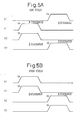
- FIGs.5A and 5B show drive signals during the sustaining discharge period in the ALIS system.
- FIG.5A shows waveforms in the odd field and FIG.5B shows those in the even field.
- a voltage Vs is applied to the electrodes Y1 and X2, X1 and Y2 are grounded, and discharge is caused to occur between X1 and Y1, and X2 and Y2, that is, at the odd-numbered display lines.
- the voltage difference between Y1 and X2, which form the even-numbered display line is zero and no discharge is caused to occur.
- a voltage Vs is applied to the electrodes X1 and Y2, Y1 and X2 are grounded, and discharge is caused to occur between Y1 and X2, and Y2 and X1, that is, at the even-numbered display lines.
- the explanation about the drive signals during the reset period and the address period is omitted.
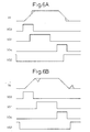
- FIG.6A shows a case where the clamp timing is advanced and FIG.6B shows a case where the clamp timing is delayed.
- the output device 40 turns on and the charge accumulated in the capacitor 39 is supplied to the electrode, and just before the increase of the potential of the electrode is completed, the signal V3 turns to L, the output device 40 turns off, and at the same time, the signal V1 turns to H, the output device 31 turns on, thus the potential of the electrode is clamped to Vs.
- the electrode is connected to the power source of voltage Vs halfway through the potential of the electrode being raised by the charge accumulated in the capacitor 39 because of the turn-on of the output device 31.
- the power for the rest of the process is supplied from the power source and a part of the charge stored on the capacitor 39 is wasted and not utilized.
- the output device 37 turns on to cause the output device 33 to turn on while the power is being recovered into the capacitor 39, the electrode is clamped to the ground level before the power is recovered sufficiently, therefore the recovery of power is not completed.
- the on/off timing of output devices 31, 33, 37, and 40 is the timing of the change of the signals V1, V2, V3, and V4 plus delay times of the drive circuits 32, 34, 38, and 41, and further plus delay times of the output devices 31, 33, 37, and 40.
- the timing of change of the signals V1, V2, V3, and V4 can be determined with a comparatively high precision, the delay times of the drive circuits 32, 34, 38, and 41, and those of the output devices 31, 33, 37, and 40 are dispersed depending on variations in characteristics of the devices used. Therefore, the power recovery rate for each PDP apparatus varies between units, becoming lower than that in an ideal case, and a problem occurs that the power consumption increases.
- the difference ⁇ Vs which is called the operation margin, of the maximum value Vs (max) and the minimum value Vs (min) in the operational range of the operating voltage Vs is reduced when the delay times of the circuit devices are dispersed and the shapes and timing of the sustaining pulses are altered. This means a deterioration in the operation stability of the apparatus.
- discharge for light emission does not take place between adjacent electrodes to which the same voltage is applied, respectively. If, however, the timing of application is shifted, a problem may arise when discharge for light emission takes place temporarily at the display lines not for display and wall-charge accumulated during the address period decreases, resulting in an abnormal display.
- FIG.5A if sustaining pulses are applied to Y1 electrodes and to X2 electrodes after a delay, a situation may occur, temporarily, in which a Y1 electrode is H and at the same time that an X2 electrode is L, and erroneous discharge for light emission may take place between a Y1 electrode and an X2 electrode. Though such erroneous discharge for light emission ceases when sustaining pulses are applied to X2 electrode, the wall-charges of Y1 electrode and X2 electrode decrease and the normal light emission for display may be reduced.
- the present invention has been developed in view of these problems and an embodiment of the present invention aims to realize a sustaining circuit in which the on/off timing and the shapes of the sustaining pulses are not shifted or changed, and a PDP apparatus with low power consumption and free from malfunctions is provided.
- the PDP apparatus of the present invention is provided with a sustaining circuit having phase adjusting circuits that adjust the timing of the changing edge of the sustaining pulse.
- a power recovery circuit can work efficiently and the power consumption will be reduced.
- the on/off timingsof the sustaining pulses applied from each sustaining circuit are optimized to each other, malfunctions or erroneous discharge can be avoided.
- the present invention is employed in a PDP apparatus equipped with the sustaining circuit having a power recovery circuit, or one employing an ALIS system.
- phase adjusting circuit In the case of the sustaining circuit equipped with a power recovery circuit, as shown in FIG.3, it is required for the phase adjusting circuit to be able to adjust the time differences from turn-on of the third output device to that of the first output device, and from turn-on of the fourth output device to that of the second output device.
- the difference of the rise timing or the fall timing between the sustaining pulse output by the first X sustaining circuit and that of the first or the second Y sustaining circuit, and the difference of the rise timing or the fall timing between the sustaining pulse output by the second X sustaining circuit and that of the first or the second Y sustaining circuit are adjusted to be lower than a predetermined value, for example, within ⁇ 30 ns.
- the optimized state can be obtained according to the actual capacity of the electrode of the PDP.
- the present invention also embraces control circuitry for a PDP.
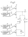
- the PDP apparatus of the present invention has the general structure as shown in FIG.4, and the first and the second X sustaining circuits 18 - O and 18 - E, and the first and the second Y sustaining circuits 19 - O and 19 - E have the structures as shown in FIG.7. Similarly, as in FIG.3, the circuits that generate the signals V1 through V4 are not shown.
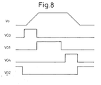
- the sustaining circuit in the embodiment is different from the structure as shown in FIG.3 in that the first phase adjusting circuit 51 to the fourth phase adjusting circuit 54 are provided in the former stage of each drive circuit 32, 34, 38, and 41. Even though the delay times of the output devices 31, 33, 37, and 40, and those of the drive circuits 32, 34, 38, and 41 are dispersed, it is still possible to achieve the optimized state of the on/off timing of the output devices 31, 33, 37, and 40 as shown in FIG.8 by adjusting the delay in the first phase adjusting circuit 51 through the fourth phase adjusting circuit 54.
- FIG.9 is a schematic showing the effect of decreasing the power consumption in the present invention.
- the power consumption increases in proportion to the number of sustaining pulses in the sustaining circuit.
- the constant of proportionality of the increase is largest when the power recovery circuit is not employed. It can be decreased considerably by employing the power recovery circuit as shown in FIG.3, and it can be decreased further along with power consumption by employing the present invention.
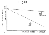
- FIG.10 is a schematic showing the improved effect of the operation margin of the present invention.
- the difference ⁇ Vs of the maximum value Vs (max) and the minimum value Vs (min) of the aforementioned operating voltage is used as the operation margin.
- the discharge current increases the operation margin decreases, but the decrease of the operation margin is smaller compared to the structure in FIG.3 when the present invention is applied.
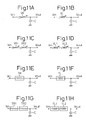
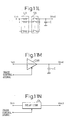
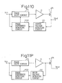
- FIGS. 11A through 11P are schematics showing the phase adjusting circuits.
- FIG.11A shows a delay circuit consisting of a variable resistor VR and a capacitor C
- FIG.11B shows that of a variable inductor VL and capacitor C
- FIG.11C shows that of a variable resistor VR1 for coarse adjustment, a variable resistor VR2 for fine adjustment, and a capacitor C
- FIG.11D shows that of a variable inductor VL1 for coarse adjustment, a variable inductor VL2 for fine adjustment
- FIG.11E shows that of a resistor TR whose resistance value can be adjusted by trimming and a capacitor C
- FIG.11F shows that of an inductor TL whose inductance value can be adjusted by trimming and a capacitor
- FIG.11G shows that of a trimming resistor TR1 for coarse adjustment, a trimming
- FIG.12 is a flow chart showing the process of setting the phase adjusting circuit.
- a delay time of an output device is measured in step 101
- a delay time of a drive circuit, which is used with the above-mentioned output device is measured in step 102
- a delay time of a phase adjusting circuit to be used together is calculated by subtracting the above-mentioned two delay times from a predetermined delay time in step 103
- the delay time of the phase adjusting circuit to be used together is set based on the calculated delay time in step 104.
- Such a process is applied to all sets. As a result, each output device turns on or off with a predetermined timing. Therefore, the power consumption can be reduced to the minimum and erroneous charge and malfunctions can be avoided.
- FIG.12 compensates for variation in delay times of the output devices and the drive circuits, and is performed before the sustaining circuit is put in the PDP apparatus. It is preferable, however, to optimize the timing of the sustaining pulses according to the PDP apparatus because there may be a variation in capacitances between electrodes of the PDP apparatus due to the manufacturing process, thus changing the time constant of the oscillation circuit in the power recovery circuit.
- FIG.13 is a flow chart showing a process of setting the delayed time of the phase adjusting circuit to the optimum value, with the variation in the PDP apparatuses driven by the sustaining circuit taken into account.
- step 111 the sustaining circuit is assembled while being set to the device including the PDP apparatus. In this step, just an operating status is required, not a complete assembly.
- a circuit for adjusting is selected among from the first X sustaining circuit 18 - O, the second X sustaining circuit 18 - E, the first Y sustaining circuit 19 - O, and the second X sustaining circuit 18 - E.
- step 113 a set for adjusting is selected, to be more specific, a phase adjusting circuit for adjusting is selected from the first to the fourth phase adjusting circuits 51 through 54.
- step 114 the waveforms relating to the selected sets of the PDP apparatus are measured, in step 115, it is established whether or not the results are within the allowed ranges with respect to the specified reference signal, and if the results are not within the allowed ranges, the phase adjusting circuit is adjusted in step 116, and steps 114 through 116 are repeated until the results are within the allowed ranges.
- step 117 whether the above-mentioned process is finished for all sets is determined, and if not, the set for adjusting is changed in step 118 and the procedure returns to step 114.
- the adjustment of the four phase adjusting circuits of the circuit for adjusting is completed, and the sustaining pulses output from the circuit turn on and off with a predetermined timing.
- step 119 whether the above-mentioned process is completed for all circuits is determined, and if not, the circuit for adjusting is changed in step 120 and the procedure returns to step 114. Finally the adjustment of all the circuits is completed.
- the timing of the sustaining pulse can be optimized by measuring the delay times of circuit devices to be used in the sustaining circuit, selecting a set in which the sum of delay times are within allowed ranges or, to be more specific, a set in which the sum of the delay times of the output devices and the drive circuit are within allowed ranges with respect to a predetermined value, and installing that set in the PDP apparatus.
- FIG.14 is a flow chart showing the manufacturing process mentioned above.
- step 131 a delay time of an output device is measured, and the devices are classified according to the delay times in step 132.
- a delay time of a drive circuit is measured in step 133 and the circuits are classified according to the delay times in step 134.
- step 135 sets are made so that the sum of the delay times for each set is equal.
- a PDP apparatus employing the ALIS system has four sustaining circuits, and each sustaining circuit has four sets of the output device and the drive circuit. That is, it is necessary to select 16 sets with the same sum of delay times because the PDP apparatus has 16 sets of the output device and the drive circuit.
- the sets of the output device and the drive circuits are set (installed) in step 136.
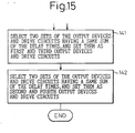
- FIG.15 is a flow chart showing the manufacturing process in this case.
- two sets of the output device and the drive circuit with the same sum of delay times are selected and used as the first output device 31 and drive circuit 32, and the third output device 40 and drive circuit 53 in step 141.
- two sets of the output device and the drive circuit with the same sum of delay times are selected and used as the second output device 33 and drive circuit 34, and the fourth output device 37 and drive circuit 54 in step 142.
- the occurrence rate of erroneous discharge is small when the difference between the sustaining pulses applied to the adjacent electrodes is within ⁇ 30 ns.
- FIG.16 is a flow chart showing 'the manufacturing process in this case.
- step 151 the capacitance of the PDP, which the sustaining circuit drives, is measured, and the best delay time of the sustaining circuit to be set thereto is calculated.
- step 152 a set of the classified output device and drive circuit is selected so that the delay time is optimized and is set in step 153.
- the on/off timing of the sustaining pulse that is influenced by the variation in delay time of the drive circuit in the sustaining circuit and that of the output devices, and the on/off timing of the output devices of the power recovery circuit can be optimized, therefore, the variation in power recovery rate in each PDP apparatus can be reduced, the power consumption on average can be also reduced, and the variation in operation margin can be improved, and moreover, the possibility of occurrence of erroneous discharge can be reduced in an ALIS-system PDP.
Landscapes
- Engineering & Computer Science (AREA)
- Physics & Mathematics (AREA)
- Power Engineering (AREA)
- Plasma & Fusion (AREA)
- Computer Hardware Design (AREA)
- General Physics & Mathematics (AREA)
- Theoretical Computer Science (AREA)
- Control Of Indicators Other Than Cathode Ray Tubes (AREA)
- Control Of Gas Discharge Display Tubes (AREA)
Applications Claiming Priority (2)
| Application Number | Priority Date | Filing Date | Title |
|---|---|---|---|
| JP2000092131A JP3644867B2 (ja) | 2000-03-29 | 2000-03-29 | プラズマディスプレイ装置及びその製造方法 |
| JP2000092131 | 2000-03-29 |
Publications (2)
| Publication Number | Publication Date |
|---|---|
| EP1139323A2 true EP1139323A2 (fr) | 2001-10-04 |
| EP1139323A3 EP1139323A3 (fr) | 2003-09-10 |
Family
ID=18607509
Family Applications (1)
| Application Number | Title | Priority Date | Filing Date |
|---|---|---|---|
| EP00309848A Withdrawn EP1139323A3 (fr) | 2000-03-29 | 2000-11-06 | Dispositif d'affichage à plasma et méthode de fabrication |
Country Status (5)
| Country | Link |
|---|---|
| US (1) | US7224329B1 (fr) |
| EP (1) | EP1139323A3 (fr) |
| JP (1) | JP3644867B2 (fr) |
| KR (1) | KR100712023B1 (fr) |
| TW (1) | TW580676B (fr) |
Cited By (12)
| Publication number | Priority date | Publication date | Assignee | Title |
|---|---|---|---|---|
| EP1341145A1 (fr) * | 2002-02-28 | 2003-09-03 | Pioneer Corporation | Circuit de commande des lignes de données d'un panneau d'affichage |
| US6781322B2 (en) | 2002-05-16 | 2004-08-24 | Fujitsu Hitachi Plasma Display Limited | Capacitive load drive circuit and plasma display apparatus |
| EP1324303A3 (fr) * | 2001-12-27 | 2006-01-11 | Fujitsu Hitachi Plasma Display Limited | Module de puissance et dispositif d'affichage |
| US7015905B2 (en) | 2003-04-10 | 2006-03-21 | Fujitsu Hitachi Plasma Display Limited | Capacitive load driving circuit driving capacitive loads such as pixels in plasma display panels and plasma display apparatus having the capacitive load driving circuit |
| US7084839B2 (en) * | 2003-02-18 | 2006-08-01 | Fujitsu Hitachi Plasma Display Limited | Pre-drive circuit, capacitive load drive circuit and plasma display apparatus |
| KR100636060B1 (ko) | 2004-07-01 | 2006-10-20 | 후지츠 히다찌 플라즈마 디스플레이 리미티드 | 표시 장치의 구동 회로 및 플라즈마 디스플레이 장치 |
| US7211963B2 (en) | 2004-05-18 | 2007-05-01 | Fujitsu Hitachi Plasma Display Limited | Capacitive load driving circuit for driving capacitive loads such as pixels in plasma display panel, and plasma display apparatus |
| KR100712023B1 (ko) * | 2000-03-29 | 2007-05-02 | 후지츠 히다찌 플라즈마 디스플레이 리미티드 | 플라즈마 디스플레이 장치 및 그 제조방법 |
| US7242399B2 (en) | 2002-03-26 | 2007-07-10 | Fujitsu Hitachi Plasma Display Limited | Capacitive load drive circuit and plasma display apparatus |
| EP1227463A3 (fr) * | 2001-01-19 | 2007-09-12 | Fujitsu Hitachi Plasma Display Limited | Dispositif d'affichage d'image par plasma et son procédé de commande |
| CN100419830C (zh) * | 2004-11-19 | 2008-09-17 | 富士通日立等离子显示器股份有限公司 | 等离子显示装置以及电容性负载驱动电路 |
| US7511441B2 (en) | 2004-06-28 | 2009-03-31 | Fujitsu Hitachi Plasma Display Limited | Semiconductor integrated circuit, drive circuit, and plasma display apparatus |
Families Citing this family (12)
| Publication number | Priority date | Publication date | Assignee | Title |
|---|---|---|---|---|
| KR100489876B1 (ko) * | 2002-06-29 | 2005-05-17 | 엘지전자 주식회사 | 플라즈마 디스플레이 패널 |
| KR100472372B1 (ko) * | 2002-08-01 | 2005-02-21 | 엘지전자 주식회사 | 플라즈마 디스플레이 패널의 구동방법 |
| KR100509602B1 (ko) * | 2002-09-27 | 2005-08-23 | 삼성에스디아이 주식회사 | 온도에 기인한 펄스 왜곡이 보상되는 플라즈마 디스플레이패널의 구동 방법 |
| KR100551051B1 (ko) * | 2003-11-27 | 2006-02-09 | 삼성에스디아이 주식회사 | 플라즈마 표시 패널의 구동 방법 및 플라즈마 표시 장치 |
| KR20050081012A (ko) * | 2004-02-12 | 2005-08-18 | 엘지전자 주식회사 | 플라즈마 표시 패널의 구동 장치 |
| KR20050112862A (ko) * | 2004-05-28 | 2005-12-01 | 삼성에스디아이 주식회사 | 플라즈마 디스플레이 패널의 구동 방법 및 그 장치 |
| JP2006058799A (ja) * | 2004-08-24 | 2006-03-02 | Fuji Electric Device Technology Co Ltd | 表示装置駆動用集積回路 |
| CN101136165A (zh) | 2006-10-12 | 2008-03-05 | 乐金电子(南京)等离子有限公司 | 等离子显示装置 |
| KR20080048893A (ko) * | 2006-11-29 | 2008-06-03 | 엘지전자 주식회사 | 플라즈마 디스플레이 장치 |
| JP2010171643A (ja) * | 2009-01-21 | 2010-08-05 | Toshiba Corp | 通信装置、制御方法および制御プログラム |
| US9378930B2 (en) * | 2009-03-05 | 2016-06-28 | Applied Materials, Inc. | Inductively coupled plasma reactor having RF phase control and methods of use thereof |
| JP4811501B2 (ja) * | 2009-06-26 | 2011-11-09 | セイコーエプソン株式会社 | 容量性負荷駆動回路、液体噴射装置及び印刷装置 |
Citations (1)
| Publication number | Priority date | Publication date | Assignee | Title |
|---|---|---|---|---|
| KR100222203B1 (ko) * | 1997-03-17 | 1999-10-01 | 구자홍 | AC 플라즈마 디스플레이 패널을 위한 에너지 리커버리(recovery) 서스테인 회로 |
Family Cites Families (29)
| Publication number | Priority date | Publication date | Assignee | Title |
|---|---|---|---|---|
| US4067047A (en) * | 1976-03-29 | 1978-01-03 | Owens-Illinois, Inc. | Circuit and method for generating gray scale in gaseous discharge panels |
| US4594588A (en) * | 1983-03-07 | 1986-06-10 | International Business Machines Corporation | Plasma display margin control |
| JPH04181809A (ja) | 1990-07-23 | 1992-06-29 | Fuji Electric Co Ltd | 集積回路装置の負荷駆動回路 |
| KR950003132B1 (ko) * | 1992-03-26 | 1995-04-01 | 삼성전관 주식회사 | 플라즈마 디스플레이 판넬의 구조 및 구동방법 |
| JP2770657B2 (ja) | 1992-06-09 | 1998-07-02 | 日本電気株式会社 | プラズマディスプレイの駆動装置 |
| JP3279704B2 (ja) * | 1993-03-19 | 2002-04-30 | 富士通株式会社 | フラットパネルディスプレイ装置の駆動方法 |
| JP2891280B2 (ja) | 1993-12-10 | 1999-05-17 | 富士通株式会社 | 平面表示装置の駆動装置及び駆動方法 |
| JP2888176B2 (ja) | 1995-07-14 | 1999-05-10 | 日本電気株式会社 | プラズマディスプレイ及びその駆動方法 |
| US6373452B1 (en) | 1995-08-03 | 2002-04-16 | Fujiitsu Limited | Plasma display panel, method of driving same and plasma display apparatus |
| JP2801893B2 (ja) | 1995-08-03 | 1998-09-21 | 富士通株式会社 | プラズマディスプレイパネル駆動方法及びプラズマディスプレイ装置 |
| US5642018A (en) * | 1995-11-29 | 1997-06-24 | Plasmaco, Inc. | Display panel sustain circuit enabling precise control of energy recovery |
| TW369674B (en) * | 1996-05-15 | 1999-09-11 | Daihen Corp | Plasma processing apparatus |
| JP3672669B2 (ja) | 1996-05-31 | 2005-07-20 | 富士通株式会社 | 平面表示装置の駆動装置 |
| JP2771527B2 (ja) * | 1997-03-28 | 1998-07-02 | 株式会社日立製作所 | 表示装置及び表示部駆動用回路 |
| US6160530A (en) * | 1997-04-02 | 2000-12-12 | Nec Corporation | Method and device for driving a plasma display panel |
| JP2976923B2 (ja) | 1997-04-25 | 1999-11-10 | 日本電気株式会社 | 容量性負荷の駆動装置 |
| JP3633761B2 (ja) | 1997-04-30 | 2005-03-30 | パイオニア株式会社 | プラズマディスプレイパネルの駆動装置 |
| JPH11327505A (ja) | 1998-05-20 | 1999-11-26 | Fujitsu Ltd | プラズマディスプレイ装置の駆動方法 |
| FR2763735B1 (fr) | 1997-05-22 | 1999-08-13 | Sgs Thomson Microelectronics | Etage de sortie de puissance pour la commande de cellules d'ecran a plasma |
| JP3897896B2 (ja) * | 1997-07-16 | 2007-03-28 | 三菱電機株式会社 | プラズマディスプレイパネルの駆動方法及びプラズマディスプレイ装置 |
| JPH11282416A (ja) | 1998-01-30 | 1999-10-15 | Mitsubishi Electric Corp | プラズマディスプレイパネルの駆動回路、その駆動方法およびプラズマディスプレイパネル装置 |
| EP1078393A4 (fr) | 1998-04-13 | 2005-04-13 | Emcore Corp | Batterie modulaire de piles solaires revouverte de verre |
| JP4240163B2 (ja) | 1998-05-21 | 2009-03-18 | 株式会社日立プラズマパテントライセンシング | プラズマディスプレイパネルの駆動方法 |
| JP3420938B2 (ja) | 1998-05-27 | 2003-06-30 | 富士通株式会社 | プラズマディスプレイパネル駆動方法および駆動装置 |
| KR100277407B1 (ko) * | 1998-06-30 | 2001-01-15 | 전주범 | 플라즈마 디스플레이 패널 텔레비전의 전력 회수방법 및 그 회로 |
| TW527576B (en) * | 1998-07-29 | 2003-04-11 | Hitachi Ltd | Display panel driving method and discharge type display apparatus |
| JP3630290B2 (ja) * | 1998-09-28 | 2005-03-16 | パイオニアプラズマディスプレイ株式会社 | プラズマディスプレイパネルの駆動方法およびプラズマディスプレイ |
| KR20010028539A (ko) * | 1999-09-21 | 2001-04-06 | 구자홍 | 에너지 회수 장치 |
| JP3644867B2 (ja) * | 2000-03-29 | 2005-05-11 | 富士通日立プラズマディスプレイ株式会社 | プラズマディスプレイ装置及びその製造方法 |
-
2000
- 2000-03-29 JP JP2000092131A patent/JP3644867B2/ja not_active Expired - Fee Related
- 2000-11-01 US US09/702,889 patent/US7224329B1/en not_active Expired - Fee Related
- 2000-11-04 TW TW089123304A patent/TW580676B/zh not_active IP Right Cessation
- 2000-11-06 EP EP00309848A patent/EP1139323A3/fr not_active Withdrawn
- 2000-11-23 KR KR1020000070074A patent/KR100712023B1/ko not_active Expired - Fee Related
Patent Citations (2)
| Publication number | Priority date | Publication date | Assignee | Title |
|---|---|---|---|---|
| KR100222203B1 (ko) * | 1997-03-17 | 1999-10-01 | 구자홍 | AC 플라즈마 디스플레이 패널을 위한 에너지 리커버리(recovery) 서스테인 회로 |
| US6111556A (en) * | 1997-03-17 | 2000-08-29 | Lg Electronics Inc. | Energy recovery sustain circuit for AC plasma display panel |
Cited By (18)
| Publication number | Priority date | Publication date | Assignee | Title |
|---|---|---|---|---|
| KR100712023B1 (ko) * | 2000-03-29 | 2007-05-02 | 후지츠 히다찌 플라즈마 디스플레이 리미티드 | 플라즈마 디스플레이 장치 및 그 제조방법 |
| EP1227463A3 (fr) * | 2001-01-19 | 2007-09-12 | Fujitsu Hitachi Plasma Display Limited | Dispositif d'affichage d'image par plasma et son procédé de commande |
| US7106320B2 (en) | 2001-12-27 | 2006-09-12 | Fujitsu Hitachi Plasma Display Limited | Power module and display device |
| EP1324303A3 (fr) * | 2001-12-27 | 2006-01-11 | Fujitsu Hitachi Plasma Display Limited | Module de puissance et dispositif d'affichage |
| US7042423B2 (en) | 2002-02-28 | 2006-05-09 | Pioneer Corporation | Driving apparatus for a display panel |
| EP1341145A1 (fr) * | 2002-02-28 | 2003-09-03 | Pioneer Corporation | Circuit de commande des lignes de données d'un panneau d'affichage |
| EP1349137A3 (fr) * | 2002-03-26 | 2008-06-11 | Fujitsu Hitachi Plasma Display Limited | Circuit d'attaque pour charges capacitives et dispositif d'affichage à plasma |
| US7242399B2 (en) | 2002-03-26 | 2007-07-10 | Fujitsu Hitachi Plasma Display Limited | Capacitive load drive circuit and plasma display apparatus |
| US6781322B2 (en) | 2002-05-16 | 2004-08-24 | Fujitsu Hitachi Plasma Display Limited | Capacitive load drive circuit and plasma display apparatus |
| US7084839B2 (en) * | 2003-02-18 | 2006-08-01 | Fujitsu Hitachi Plasma Display Limited | Pre-drive circuit, capacitive load drive circuit and plasma display apparatus |
| EP1467343A3 (fr) * | 2003-04-10 | 2006-10-04 | Fujitsu Hitachi Plasma Display Limited | Circuits d' attaque pour charge capacitive et appareils d'affichage à plasma avec temporisation ameliorée et consommation de puissance réduite |
| US7015905B2 (en) | 2003-04-10 | 2006-03-21 | Fujitsu Hitachi Plasma Display Limited | Capacitive load driving circuit driving capacitive loads such as pixels in plasma display panels and plasma display apparatus having the capacitive load driving circuit |
| CN100359546C (zh) * | 2003-04-10 | 2008-01-02 | 富士通日立等离子显示器股份有限公司 | 电容性负载驱动电路 |
| US7211963B2 (en) | 2004-05-18 | 2007-05-01 | Fujitsu Hitachi Plasma Display Limited | Capacitive load driving circuit for driving capacitive loads such as pixels in plasma display panel, and plasma display apparatus |
| US7511441B2 (en) | 2004-06-28 | 2009-03-31 | Fujitsu Hitachi Plasma Display Limited | Semiconductor integrated circuit, drive circuit, and plasma display apparatus |
| KR100636060B1 (ko) | 2004-07-01 | 2006-10-20 | 후지츠 히다찌 플라즈마 디스플레이 리미티드 | 표시 장치의 구동 회로 및 플라즈마 디스플레이 장치 |
| CN100419830C (zh) * | 2004-11-19 | 2008-09-17 | 富士通日立等离子显示器股份有限公司 | 等离子显示装置以及电容性负载驱动电路 |
| CN101261802B (zh) * | 2004-11-19 | 2012-04-18 | 日立等离子显示器股份有限公司 | 等离子显示装置 |
Also Published As
| Publication number | Publication date |
|---|---|
| KR20010093628A (ko) | 2001-10-29 |
| JP3644867B2 (ja) | 2005-05-11 |
| JP2001282181A (ja) | 2001-10-12 |
| US7224329B1 (en) | 2007-05-29 |
| EP1139323A3 (fr) | 2003-09-10 |
| KR100712023B1 (ko) | 2007-05-02 |
| TW580676B (en) | 2004-03-21 |
Similar Documents
| Publication | Publication Date | Title |
|---|---|---|
| EP1139323A2 (fr) | Dispositif d'affichage à plasma et méthode de fabrication | |
| US6784859B2 (en) | Plasma display drive method | |
| US6680581B2 (en) | Apparatus and method for driving plasma display panel | |
| JP5015380B2 (ja) | Pdpのエネルギー回収装置及びその方法と、それを利用した高速アドレッシング方法 | |
| US6803889B2 (en) | Plasma display device and method for controlling the same | |
| US7102598B2 (en) | Predrive circuit, drive circuit and display device | |
| US20050168410A1 (en) | Drive circuit and drive method | |
| US20020030642A1 (en) | Energy recovery circuit for plasma display panel | |
| JP3568098B2 (ja) | 表示パネルの駆動装置 | |
| EP1467343B1 (fr) | Circuits d' attaque pour charge capacitive et appareils d'affichage à plasma avec temporisation ameliorée et consommation de puissance réduite | |
| US20030001513A1 (en) | Plasma display apparatus | |
| US7050022B2 (en) | Display and its driving method | |
| US7136032B2 (en) | Plasma display apparatus | |
| US6927751B2 (en) | Plasma display apparatus having a driver protecting portion | |
| JP4240241B2 (ja) | 表示装置の駆動回路 | |
| KR100330032B1 (ko) | 플라즈마 디스플레이 패널의 전력회수장치 및 이를 이용한고속 어드레싱 방법 | |
| US7102597B2 (en) | Driver device for driving capacitive light emitting elements | |
| US20050219158A1 (en) | Plasma display and method for driving the same | |
| KR100629833B1 (ko) | 용량성 부하 구동 회로 및 플라즈마 디스플레이 장치 | |
| US7015649B2 (en) | Apparatus and method for driving capacitive load, and processing program embodied in a recording medium for driving capacitive load | |
| JPH1091088A (ja) | マトリクス表示装置 | |
| EP1526497A2 (fr) | Circuit d'attaque pour un élément capacitif émetteur de lumière | |
| JP2000250484A (ja) | 表示パネルの駆動装置 | |
| JP2004157553A (ja) | プラズマディスプレイ装置の製造方法 | |
| KR100748983B1 (ko) | 플라즈마 디스플레이 장치 |
Legal Events
| Date | Code | Title | Description |
|---|---|---|---|
| PUAI | Public reference made under article 153(3) epc to a published international application that has entered the european phase |
Free format text: ORIGINAL CODE: 0009012 |
|
| AK | Designated contracting states |
Kind code of ref document: A2 Designated state(s): AT BE CH CY DE DK ES FI FR GB GR IE IT LI LU MC NL PT SE TR |
|
| AX | Request for extension of the european patent |
Free format text: AL;LT;LV;MK;RO;SI |
|
| PUAL | Search report despatched |
Free format text: ORIGINAL CODE: 0009013 |
|
| AK | Designated contracting states |
Kind code of ref document: A3 Designated state(s): AT BE CH CY DE DK ES FI FR GB GR IE IT LI LU MC NL PT SE TR |
|
| AX | Request for extension of the european patent |
Extension state: AL LT LV MK RO SI |
|
| 17P | Request for examination filed |
Effective date: 20031124 |
|
| AKX | Designation fees paid |
Designated state(s): DE FR GB |
|
| RAP1 | Party data changed (applicant data changed or rights of an application transferred) |
Owner name: HITACHI PLASMA DISPLAY LIMITED |
|
| STAA | Information on the status of an ep patent application or granted ep patent |
Free format text: STATUS: THE APPLICATION IS DEEMED TO BE WITHDRAWN |
|
| 18D | Application deemed to be withdrawn |
Effective date: 20090324 |