EP1142122B1 - Convertisseur numerique-analogique - Google Patents
Convertisseur numerique-analogique Download PDFInfo
- Publication number
- EP1142122B1 EP1142122B1 EP00971357A EP00971357A EP1142122B1 EP 1142122 B1 EP1142122 B1 EP 1142122B1 EP 00971357 A EP00971357 A EP 00971357A EP 00971357 A EP00971357 A EP 00971357A EP 1142122 B1 EP1142122 B1 EP 1142122B1
- Authority
- EP
- European Patent Office
- Prior art keywords
- conversion elements
- signal
- output terminal
- conversion
- mentioned
- Prior art date
- Legal status (The legal status is an assumption and is not a legal conclusion. Google has not performed a legal analysis and makes no representation as to the accuracy of the status listed.)
- Expired - Lifetime
Links
- 238000006243 chemical reaction Methods 0.000 claims abstract description 152
- 238000007493 shaping process Methods 0.000 abstract description 8
- 238000012935 Averaging Methods 0.000 description 9
- 238000000034 method Methods 0.000 description 8
- 238000013139 quantization Methods 0.000 description 8
- 108010076504 Protein Sorting Signals Proteins 0.000 description 3
- 230000009977 dual effect Effects 0.000 description 3
- 238000005070 sampling Methods 0.000 description 3
- 230000000694 effects Effects 0.000 description 2
- XUIMIQQOPSSXEZ-UHFFFAOYSA-N Silicon Chemical compound [Si] XUIMIQQOPSSXEZ-UHFFFAOYSA-N 0.000 description 1
- 230000002349 favourable effect Effects 0.000 description 1
- 238000005259 measurement Methods 0.000 description 1
- 229910052710 silicon Inorganic materials 0.000 description 1
- 239000010703 silicon Substances 0.000 description 1
Images



Classifications
-
- H—ELECTRICITY
- H03—ELECTRONIC CIRCUITRY
- H03M—CODING; DECODING; CODE CONVERSION IN GENERAL
- H03M1/00—Analogue/digital conversion; Digital/analogue conversion
- H03M1/06—Continuously compensating for, or preventing, undesired influence of physical parameters
- H03M1/0617—Continuously compensating for, or preventing, undesired influence of physical parameters characterised by the use of methods or means not specific to a particular type of detrimental influence
- H03M1/0634—Continuously compensating for, or preventing, undesired influence of physical parameters characterised by the use of methods or means not specific to a particular type of detrimental influence by averaging out the errors, e.g. using sliding scale
- H03M1/0656—Continuously compensating for, or preventing, undesired influence of physical parameters characterised by the use of methods or means not specific to a particular type of detrimental influence by averaging out the errors, e.g. using sliding scale in the time domain, e.g. using intended jitter as a dither signal
- H03M1/066—Continuously compensating for, or preventing, undesired influence of physical parameters characterised by the use of methods or means not specific to a particular type of detrimental influence by averaging out the errors, e.g. using sliding scale in the time domain, e.g. using intended jitter as a dither signal by continuously permuting the elements used, i.e. dynamic element matching
- H03M1/0665—Continuously compensating for, or preventing, undesired influence of physical parameters characterised by the use of methods or means not specific to a particular type of detrimental influence by averaging out the errors, e.g. using sliding scale in the time domain, e.g. using intended jitter as a dither signal by continuously permuting the elements used, i.e. dynamic element matching using data dependent selection of the elements, e.g. data weighted averaging
-
- H—ELECTRICITY
- H03—ELECTRONIC CIRCUITRY
- H03M—CODING; DECODING; CODE CONVERSION IN GENERAL
- H03M1/00—Analogue/digital conversion; Digital/analogue conversion
- H03M1/12—Analogue/digital converters
- H03M1/1205—Multiplexed conversion systems
-
- H—ELECTRICITY
- H03—ELECTRONIC CIRCUITRY
- H03M—CODING; DECODING; CODE CONVERSION IN GENERAL
- H03M1/00—Analogue/digital conversion; Digital/analogue conversion
- H03M1/66—Digital/analogue converters
- H03M1/74—Simultaneous conversion
- H03M1/742—Simultaneous conversion using current sources as quantisation value generators
- H03M1/747—Simultaneous conversion using current sources as quantisation value generators with equal currents which are switched by unary decoded digital signals
Definitions
- This invention relates to a digital to analog converter for converting a multibit digital input signal into an analog output signal as defined by the preamble of claim 1.
- a digital to analog converter of this kind is e.g. known from the article: "Linearity Enhancement of Multibit Delta Sigma A/D and D/A Converters Using Data Weighted Averaging" by R.T. Baird and T.S. Fiez in IEEE Transactions on Circuits and Systems-II: analog and digital signal processing, Vol. 42, No. 12, pp. 753-762, December 1995.
- a digital to analog converter of this kind is also disclosed in F.Chen et al, "A multi-bit DAC with dynamic element matching techniques," IEEE Proceedings of the Custom Integrated Circuit Conference, Boston, May 3-6, 1992, vol. 14, 3 May 1992 (1992-05-03), pages 1621-1624, Boston, New York, USA.
- the quantization noise that is produced by single-bit converters is placed outside the frequency hand of interest by these oversampling and noise-shaping converters, the total amount of quantization noise is very large, as only one bit is used in the conversion. In converters where an extremely high-resolution conversion is required, such as geoseismic measurements or high-resolution audio, the quantization noise produced by these single-bit converters can be too large. Also, in conveners for very large bandwidths, such as converters for video signals, the quantization noise produced by these single-bit converters can be too large, as the oversampling ratio in this type of converter is limited, due to the relatively large bandwidth of the input signal.
- multibit converters are preferred over single-bit converters.
- the quantization-noise level of the multibit quantizers is inherently lower than that of single-bit quantizers (the theoretical signal to noise ratio of the system improves by approximately 6dB per bit).
- multibit converters also have the advantage of being less sensitive to sample-clock jitter and intersymbol interference.
- DWA Data Weighted Averaging
- the present invention has for its object to provide a digital to analog converter which is, compared with the above referenced article, in this respect improved and the digital to analog converter of the present invention is therefore characterized by the characterizing portion of claim 1.
- the noise reduction of this converter is mainly based on the following: when the converter has to deliver a value close to "zero", no or only few elements are selected in each of the two sets to deliver the analog output. As the contribution of the selected elements is relatively small, as compared to the full-scale output signal, the noise at the output of this converter can be much smaller. Therefore, the dynamic range of such a converter can be much larger than that of many other converters.
- the shaping of the linearity errors by the dynamic element matching algorithm appeats to be less efficient than with a converter of only one set of conversion elements for both the positive and the negative signal excursions. This is caused by the fact that the dynamic element matching algorithm that is applied to the "positive" set of element stops when a negative signal excursion is made, because no elements of this set of elements are selected for contributing to the output signal and equally that the dynamic element matching algorithm for the "negative" set of elements stops when a positive signal excursion is made.
- the digital to analog converter of the present invention may be further characterized in that the first mentioned selection logic additionally selects, from said first mentioned set of conversion elements, a number of excess conversion elements for connection to the output terminal and that the second selection logic additionally selects, from the second set of conversion elements, an equal number of excess conversion elements for connection to the output terminal.
- the selection of excess conversion elements cause the dynamic element matching algorithms to continue their operation, thereby preventing the occurrence of low-frequency mismatch errors.
- the number of excess conversion elements during positive signal excursions may be different from the number of excess conversion elements during negative signal excursions. It is even possible that the number of excess elements differ from sample to sample.
- the number of excess conversion elements is constant and equal to 1 both during positive and during negative signal excursions. This choice enables good dynamic element matching and good thermal noise performance, as only few conversion elements are connected to the output of the converter when small signals have to be converted. When the number of excess elements is larger than 1, more noise is added to the output. However in some cases it can be favourable for the performance of the dynamic element matching algorithm to choose the number of excess conversion elements to be larger than 1.
- signal-conversion element is used to identify those conversion elements, which are selected to constitute the analog output signal, in contradistinction to the "excess conversion elements” which are selected to avoid the temporary stops of the dynamic element matching algorithm.
- this additional problem may be solved in a digital to analog converter with a differential analog output without increasing the number of sets of elements and the digital to analog converter of the present invention may therefore be further characterized in that the first mentioned selection logic additionally controls the second set of conversion elements, whereby, simultaneously with the connection of the first mentioned number of signal-conversion elements from the first set to the first mentioned output terminal, an equal number of signal-conversion elements is selected from the second set of conversion elements for connection to the second output terminal and that the second selection logic additionally controls the first mentioned set of conversion elements, whereby, simultaneously with the connection of the second number of signal-conversion elements from the second set to the first mentioned output terminal, an equal number of signal-conversion elements from the first set is selected for connection to the second output terminal.
- the dual-set differential-output analog to digital converter of the present invention may be further characterized in that the first mentioned selection logic additionally selects, from said first mentioned set of conversion elements a first number of excess conversion elements for connection to the first mentioned output terminal, that the first mentioned selection logic additionally selects, from said second set of conversion elements a second number of excess conversion elements for connection to the second output terminal, that the second selection logic additionally selects, from said second set of conversion elements a third number of excess conversion elements for connection to the first mentioned output terminal, that the second selection logic additionally selects, from said first mentioned set of conversion elements a fourth number of excess conversion elements for connection to the second output terminal and that the sum of the first number of excess conversion elements and the second number of excess conversion elements is equal to the sum of the third number of excess conversion elements and the fourth number of excess conversion elements.
- the dynamic element matching algorithms of the two selection logics run through the set of conversion elements with different velocities, which implies that from time to time both selection logics are scheduled to simultaneously select the same conversion element.
- This problem may e.g. be solved by causing one of the selection logics to shift its selection to the first next conversion element which is not selected by the other selection logic.
- such solution is a violation of the proper operation of the dynamic element matching algorithm, because a conversion element with the wrong error is selected and moreover it is difficult to implement.
- the digital to analog converter of figure 1 comprises a first conversion element selection logic 1 and a second conversion element selection logic 2, which are both controlled by a multibit digital input signal Si.
- the input signal Si has n+1 bits, of which one bit represents the sign (positive or negative) of the signal and the remaining n bits represent the magnitude of the signal.
- the sign bit controls an AND gate 3 which passes the n magnitude bits to the selection logic 1 when the sign bit is 1.
- the sign bit controls an inverter and AND gate 4 which passes the magnitude bits to the selection logic 2 when the sign bit is zero.
- the selection logic 1 is connected through a plurality of m lines to a first set 5 of m selectable conversion elements whereby each of the m conversion elements is controlled by one of the m lines.
- the conversion elements of the sets 5 and 6 are preferably constituted as current sources (as shown in figure 1) whereby the current sources of the set 5 are current supplying sources and those of the set 6 are current sinking sources.
- current sources as shown in figure 1
- voltage sources or capacitances it is also possible to use e.g. voltage sources or capacitances as conversion elements.
- the number m of selectable conversion elements per set is at least equal to 2 n -1 and the primary function of each selection logic is to convert the value represented by the magnitude bits of the input signal to a corresponding number of selected lines and of selected conversion elements. Therefore, when the value represented by the input signal is +K1, which means that the sign bit is 1 and the n remaining bits of the input signal represent the magnitude K1, then the selection logic 1 makes K1 of its m output lines high so that K1 current sources of the set 5 are selected. The summed current K1 of these selected current sources is fed to an output terminal 7. It may be observed that the addition "+L" to the currents K1 and K2 in figure 1 will be explained with reference to figure 2b.
- the selection logic 2 makes K2 of its output lines high so that K2 current sources of the set 6 are selected.
- the summed current K2 of these selected current sources is sunk from the output terminal 7. Therefore the total analog output current derived from the output terminal 7 is K1-K2.
- this analog output current is fed to an operational amplifier which is fed back through a resistor. This arrangement converts the analog output current into an analog output voltage. It is noted that the currents of the not-selected sources of the sets 5 and 6 are dumped to ground.
- the alternative, namely switching the sources on and off, is not preferred because the switching off of a current source gives substantially more delay, with less steep edges, than redirecting the current of the source.
- the main advantage of the dual-set digital to analog converter is that at low values of the signal to be converted, i.e. at signal values at which noise is most noticeable, only a low amount of current sources is selected, with a correspondingly low amount of noise contributed by these selected sources. For instance, when the input value is +1, only one current source of set 5 is selected and when the input value is -1, only one source of set 6 is selected.
- Each of the two selection logics 1 and 2 carries out a dynamic element matching algorithm, with the object to reduce non-linear distortion of the signal and to shape the noise, which is caused by the mismatch between the current sources, to higher frequencies outside the frequency band of interest.
- a simple, efficient and well known dynamic element matching algorithm which is called “Data Weighted Averaging” (DWA) is used in the embodiment of figure 1 and illustrated in the selection scheme of figure 2a for a particular input signal sequence 3,4,2,5,4,-3,-4,-6,-1.
- DWA Data Weighted Averaging
- the left column shows the selection scheme for the current sources in the "positive" set 5
- the right column shows the selection scheme for the current sources in the "negative” set 6. The selected current sources are displayed blocked and the non-selected current sources are displayed blank.
- the number of selected conversion elements corresponds with the magnitude of the input signal to be converted. However, instead of restarting each conversion with the first current source, each conversion is now started with the current source next to the last source selected during the previous conversion. When during a conversion, the last current source in the row of sources is selected, the conversion continues, in a cyclically permuting fashion, with the first one. In figure 2a 12 conversion elements are shown, but in practice each other number of conversion elements per set may be used, e.g. 31.
- the "Data Weighted Averaging" is a preferred algorithm for selecting the conversion elements because it ensures that all the conversion elements come in for selection equally long and that the conversion elements come in for selection as frequently as possible.
- K1+L sources are selected in the "positive” set 5 and L sources in the "negative” set 6.
- K2+L sources selected from the "negative” set 6 and L sources from the "positive” set 5.
- K1+L sources selected and in set 6 K2+L sources, where K1 is zero during negative signal excursions and K2 is zero during positive signal excursions.
- the output of the digital to analog converter is still K1-K2., but, due to the L excess sources, the dynamic element matching algorithm of the "positive” set is continued during negative signal excursions and the algorithm of the "negative” set is continued during positive signal excursions, thereby preventing low-frequency mismatch errors.
- the parameter L can of course be varied, but preferably L is equal to 1 because this enables good dynamic element matching and good thermal noise performance, as the number of sources selected is still low at low signal values.
- the converter of figure 3 comprises a first set of conversion elements 11 and a second set 12.
- the conversion elements of the first set 11 are again selected by the selection logic 1 but they are simultaneously selected by the selection logic 2. Therefore, while selection logic 1 selects K1 elements of the set 11 according to its dynamic element matching algorithm (as it did in the arrangement of figure 1), the selection logic 2 selects K2 elements of the set 11 according to the dynamic element matching algorithm of selection logic 2. (The references to elements L1, L2, L3, and L4 in figure 3 will be discussed in the next paragraph).
- the currents of the K1 sources selected by logic 1 are directed, to a first output terminal 13 and the currents of the K2 sources selected by selection logic 2, are directed to a second output terminal 14.
- the conversion elements of the set 12 are selected by both the selection logic 1 and the selection logic 2.
- the currents of the K2 sources, selected by selection logic 2 are sunk from the first output terminal 13 and the currents of the K1 sources, selected by selection logic 1, are sunk from the second output terminal 14. Consequently, the first output terminal delivers a current K1-K2 and the second output terminal delivers a current K2-K1, so that a real differential output signal 2(K1-K2) is obtained from between the two mentioned output terminals.
- each of the m lines from the selection logic 1 or 2 selects one of the m conversion elements in a set. This means that in the arrangement of figure 3 the selection of each conversion element is controlled by two lines, one from logic 1 and one from logic 2. It is further noted that each conversion element can be in one of three situations: each element of set 11 can be selected by the algorithm of logic 1, in which case it is connected to the output terminal 13 , or it can be selected by the algorithm of logic 2, in which case it is connected to the output terminal 14, or it can be selected by neither one of the two algorithms, in which case its current is dumped to ground.
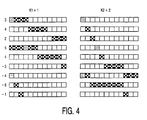
- the selected elements are blocked, the originally non-selected elements are blank and the elements of which the selection is cancelled are shaded.
- Subtracting the two output currents gives the differential output signal 2i(K1-K2) which is free from di-asymmetry errors.
- Adding the two output currents gives: 2di(K1+K2+2L) which shows that the di-asymmetry errors only appear in the common mode of the output signal.
- FIG. 5 shows a conversion element selection scheme for the arrangement of figure 3, with a conversion frequency which is twice the sampling frequency and with the same input signal sequence as used in figures 2 and 4.
Landscapes
- Engineering & Computer Science (AREA)
- Theoretical Computer Science (AREA)
- Analogue/Digital Conversion (AREA)
Abstract
Claims (5)
- Convertisseur numérique-analogique pour convertir un signal d'entrée numérique à bits multiples en un signal de sortie analogique, le convertisseur comprenant un ensemble d'éléments de conversion pratiquement égaux d'une polarité et une logique de sélection d'élément de conversion pour sélectionner, en réponse au signal d'entrée numérique à bits multiples, à partir dudit ensemble d'éléments de conversion un nombre (K1) d'éléments de conversion de signal pour connecter à une borne de sortie, la logique de sélection étant adaptée pour exécuter un algorithme d'adaptation dynamique d'élément, où le convertisseur comprend en outre un second ensemble (6) d'éléments de conversion de polarité opposée pratiquement égaux pour des excursions du signal de sortie qui sont opposées aux excursions du signal de sortie obtenues par l'ensemble mentionné en premier (5) d'éléments de conversion et une seconde logique de sélection d'élément de conversion (2) pour sélectionner, en réponse au signal d'entrée numérique à bits multiples (Si), à partir dudit second ensemble (6) d'éléments de conversion un second nombre (K2) d'éléments de conversion de signal pour connexion à ladite borne de sortie (7), la seconde logique de sélection (2) étant également adaptée pour exécuter un algorithme d'adaptation dynamique d'élément, caractérisé en ce que la logique de sélection mentionnée en premier (1) sélectionne en plus, à partir dudit ensemble mentionné en premier (5) des éléments de conversion, un nombre (L) d'éléments de conversion en excès pour connexion à la borne de sortie (7) et en ce que la seconde logique de sélection (2) sélectionne en plus, à partir du second ensemble (6) d'éléments de conversion, un nombre égal (L) d'éléments de conversion en excès pour connexion à la borne de sortie analogique (7).
- Convertisseur numérique-analogique selon la revendication 1 pour convertir un signal d'entrée numérique à bits multiples en un signal de sortie analogique différentiel, caractérisé en ce que la logique de sélection mentionnée en premier (1) contrôle en plus le second ensemble (12) d'éléments de conversion, où, simultanément avec la connexion du nombre mentionné en premier (K1) d'éléments de conversion à partir du premier ensemble (11) à la borne de sortie mentionnée en premier (13), un nombre égal d'éléments de conversion de signal est sélectionné à partir du second ensemble (12) d'éléments de conversion pour connexion à une seconde borne de sortie (14) et en ce que la seconde logique de sélection (2) contrôle en plus l'ensemble mentionné en premier (11) d'éléments de conversion, où, simultanément avec la connexion du second nombre (K2) d'éléments de conversion de signal à partir du second ensemble (12) à la borne de sortie mentionnée en premier (13), un nombre égal d'éléments de conversion de signal du premier ensemble (11) est sélectionné pour connexion à la seconde borne de sortie (14).
- Convertisseur numérique-analogique selon la revendication (2), caractérisé en ce que la logique de sélection mentionnée en premier (1) sélectionne en plus, à partir dudit ensemble mentionné en premier d'éléments de conversion (11) un premier nombre (L1) d'éléments de conversion en excès pour connexion à la borne de sortie mentionnée en premier (13), en ce que la logique de sélection mentionnée en premier (1) sélectionne en plus, à partir dudit second ensemble d'éléments de conversion (12) un deuxième nombre (L2) d'éléments de conversion en excès pour connexion à la seconde borne de sortie (16), en ce que la seconde logique de sélection (2) sélectionne en plus, à partir dudit second ensemble d'éléments de conversion (12) un troisième nombre (L3) d'éléments de conversion en excès pour connexion à la borne de sortie mentionnée en premier (13), en ce que la seconde logique de sélection (2) sélectionne en plus, à partir dudit ensemble mentionné en premier d'éléments de conversion (11) un quatrième nombre (L4) d'éléments de conversion en excès pour connexion à la seconde borne de sortie (14) et en ce que la somme du premier nombre (L1) d'éléments de conversion en excès et du deuxième nombre (L2) d'éléments de conversion en excès est égale à la somme du troisième nombre (L3) d'éléments de conversion en excès et du quatrième nombre (L4) d'éléments de conversion en excès.
- Convertisseur numérique-analogique selon la revendication 1 ou 3, caractérisé en ce que chacun des nombres mentionnés d'éléments de conversion en excès est égal à 1.
- Convertisseur numérique-analogique selon la revendication 3, caractérisé par des moyens pour comparer le fonctionnement des deux logiques de sélection entre eux pour identifier tout élément de conversion qui est ordonnancé pour une sélection simultanée par les deux logiques de sélection et pour annuler la sélection d'un tel élément de conversion par chacun des deux logiques de sélection.
Priority Applications (1)
| Application Number | Priority Date | Filing Date | Title |
|---|---|---|---|
| EP00971357A EP1142122B1 (fr) | 1999-10-27 | 2000-10-09 | Convertisseur numerique-analogique |
Applications Claiming Priority (4)
| Application Number | Priority Date | Filing Date | Title |
|---|---|---|---|
| EP99203538 | 1999-10-27 | ||
| EP99203538 | 1999-10-27 | ||
| PCT/EP2000/009952 WO2001031793A1 (fr) | 1999-10-27 | 2000-10-09 | Convertisseur numerique-analogique |
| EP00971357A EP1142122B1 (fr) | 1999-10-27 | 2000-10-09 | Convertisseur numerique-analogique |
Publications (2)
| Publication Number | Publication Date |
|---|---|
| EP1142122A1 EP1142122A1 (fr) | 2001-10-10 |
| EP1142122B1 true EP1142122B1 (fr) | 2006-09-27 |
Family
ID=8240785
Family Applications (1)
| Application Number | Title | Priority Date | Filing Date |
|---|---|---|---|
| EP00971357A Expired - Lifetime EP1142122B1 (fr) | 1999-10-27 | 2000-10-09 | Convertisseur numerique-analogique |
Country Status (6)
| Country | Link |
|---|---|
| US (1) | US6426715B1 (fr) |
| EP (1) | EP1142122B1 (fr) |
| JP (1) | JP4583689B2 (fr) |
| CN (1) | CN1166063C (fr) |
| DE (1) | DE60030950T2 (fr) |
| WO (1) | WO2001031793A1 (fr) |
Families Citing this family (23)
| Publication number | Priority date | Publication date | Assignee | Title |
|---|---|---|---|---|
| DE10136440A1 (de) * | 2001-07-26 | 2003-02-13 | Bosch Gmbh Robert | Anordnung und Verfahren zur Digital-/Analogumsetzung |
| AU2002356359A1 (en) * | 2001-12-18 | 2003-06-30 | Koninklijke Philips Electronics N.V. | Digital to analogue converter |
| US7042378B2 (en) * | 2002-01-30 | 2006-05-09 | Koninklijke Philips Electronics N.V. | Circuit with a digital to analog converter |
| US6639534B2 (en) * | 2002-02-14 | 2003-10-28 | Silicon Laboratories, Inc. | Digital-to-analog converter switching circuitry |
| CN100514863C (zh) * | 2002-09-26 | 2009-07-15 | 阿纳洛格装置公司 | 集成的数字校准电路和数模转换器(dac) |
| DE60306110D1 (de) * | 2003-04-07 | 2006-07-27 | St Microelectronics Srl | Verfahren zur Erzeugung einer Schaltsequenz für eine gleichförmig gewichtete Anordnung leitender Zweige und zugehöriger Thermometer-dekodierter Digital/Analog-Wandler |
| DE10331545A1 (de) * | 2003-07-11 | 2005-02-10 | Infineon Technologies Ag | Digital-Analog-Wandler und Verfahren zur Digital-Analog-Wandlung |
| US7199741B2 (en) * | 2003-10-24 | 2007-04-03 | Infineon Technologies Ag | Method for digital/analog conversion and corresponding digital/analog converter device |
| DE102004005138B9 (de) * | 2003-10-24 | 2010-11-25 | Infineon Technologies Ag | Verfahren zur Digital/Analog-Wandlung und entsprechende Digital/Analog-Wandlervorrichtung |
| US7245245B2 (en) * | 2005-10-11 | 2007-07-17 | Via Technologies Inc. | Digitizer and related charge pump circuit |
| CN102684699B (zh) | 2006-05-21 | 2015-03-18 | 株式会社特瑞君思半导体 | 声音再现用数据变换装置 |
| JP4836736B2 (ja) * | 2006-09-29 | 2011-12-14 | 株式会社東芝 | デジタル・アナログ変換回路 |
| JP2009296391A (ja) * | 2008-06-05 | 2009-12-17 | New Japan Radio Co Ltd | ダイナミック・エレメント・マッチング方法 |
| JP5396588B2 (ja) | 2008-06-16 | 2014-01-22 | 株式会社 Trigence Semiconductor | デジタルスピーカー駆動装置,デジタルスピーカー装置,アクチュエータ,平面ディスプレイ装置及び携帯電子機器 |
| CN101562454B (zh) * | 2009-05-12 | 2012-07-25 | 凌阳多媒体股份有限公司 | 动态元件匹配的数字/模拟转换系统及积分三角调制装置 |
| EP2391014B1 (fr) * | 2009-12-09 | 2017-12-27 | Trigence Semiconductor, Inc. | Dispositif de selection |
| WO2011074341A1 (fr) | 2009-12-16 | 2011-06-23 | 株式会社 Trigence Semiconductor | Système acoustique |
| CN102664632A (zh) * | 2012-04-30 | 2012-09-12 | 珠海市杰理科技有限公司 | 数模转换器 |
| US8643525B1 (en) * | 2013-01-03 | 2014-02-04 | Avnera Corporation | Multiple output dynamic element matching algorithm with mismatch noise shaping for digital to analog converters |
| US9543974B1 (en) | 2015-09-18 | 2017-01-10 | Analog Devices, Inc. | Reducing switching error in data converters |
| US9780798B1 (en) * | 2016-11-01 | 2017-10-03 | Texas Instruments Incorporated | Digital modulator entropy source |
| US10009686B1 (en) * | 2017-04-17 | 2018-06-26 | Cirrus Logic, Inc. | Fully-differential current digital-to-analog converter |
| WO2021131909A1 (fr) | 2019-12-27 | 2021-07-01 | ローム株式会社 | Convertisseur n/a, circuit amplificateur audio, dispositif électronique et système audio embarqué utilisant un convertisseur n/a et un circuit amplificateur audio |
Family Cites Families (8)
| Publication number | Priority date | Publication date | Assignee | Title |
|---|---|---|---|---|
| NL7405441A (nl) | 1974-04-23 | 1975-10-27 | Philips Nv | Nauwkeurige stroombronschakeling. |
| NL8003948A (nl) | 1980-07-09 | 1982-02-01 | Philips Nv | Digitaal-analoog omzetter. |
| NL8703128A (nl) * | 1987-12-24 | 1989-07-17 | Philips Nv | Digitaal-analoog-omzetter. |
| US4972188A (en) * | 1989-09-15 | 1990-11-20 | International Business Machines Corporation | Push pull double digital-to-analog converter |
| GB9209498D0 (en) * | 1992-05-01 | 1992-06-17 | Univ Waterloo | Multi-bit dac with dynamic element matching |
| JP3469326B2 (ja) * | 1994-08-16 | 2003-11-25 | バー−ブラウン・コーポレーション | デジタル−アナログ変換器 |
| US5689259A (en) * | 1995-07-21 | 1997-11-18 | Exar Corporation | Differental D/A converter with N-bits plus sign |
| US6211805B1 (en) * | 1999-09-08 | 2001-04-03 | Texas Instruments Incorporated | Noise shaping dynamic element mismatch in analog to digital converters |
-
2000
- 2000-10-09 EP EP00971357A patent/EP1142122B1/fr not_active Expired - Lifetime
- 2000-10-09 CN CNB008043175A patent/CN1166063C/zh not_active Expired - Fee Related
- 2000-10-09 DE DE60030950T patent/DE60030950T2/de not_active Expired - Lifetime
- 2000-10-09 WO PCT/EP2000/009952 patent/WO2001031793A1/fr not_active Ceased
- 2000-10-09 JP JP2001533633A patent/JP4583689B2/ja not_active Expired - Fee Related
- 2000-10-27 US US09/698,762 patent/US6426715B1/en not_active Expired - Lifetime
Non-Patent Citations (1)
| Title |
|---|
| F. CHEN ET AL.: "A MULTI-BIT DAC WITH DYNAMIC ELEMENT MATCHING TECHNIQUES", IEEE PROCEEDINGS OF THE CUSTOM INTEGRATED CIRCUITS CONFERENCE, BOSTON, MAY 3 - 6, 1992, vol. 14, 3 May 1992 (1992-05-03), NEW YORK, USA, pages 1621 - 1624, XP000034092 * |
Also Published As
| Publication number | Publication date |
|---|---|
| EP1142122A1 (fr) | 2001-10-10 |
| DE60030950T2 (de) | 2007-05-24 |
| CN1166063C (zh) | 2004-09-08 |
| WO2001031793A1 (fr) | 2001-05-03 |
| CN1341292A (zh) | 2002-03-20 |
| US6426715B1 (en) | 2002-07-30 |
| JP2003513502A (ja) | 2003-04-08 |
| JP4583689B2 (ja) | 2010-11-17 |
| DE60030950D1 (de) | 2006-11-09 |
Similar Documents
| Publication | Publication Date | Title |
|---|---|---|
| EP1142122B1 (fr) | Convertisseur numerique-analogique | |
| US5221926A (en) | Circuit and method for cancelling nonlinearity error associated with component value mismatches in a data converter | |
| US6734818B2 (en) | Digital cancellation of D/A converter noise in pipelined A/D converters | |
| US6583742B1 (en) | Digital to analogue converter with dynamic element matching | |
| Baird et al. | Linearity enhancement of multibit/spl Delta//spl Sigma/A/D and D/A converters using data weighted averaging | |
| US5977899A (en) | Digital-to-analog converter using noise-shaped segmentation | |
| US5936562A (en) | High-speed sigma-delta ADCs | |
| US5982313A (en) | High speed sigma-delta analog-to-digital converter system | |
| US5990819A (en) | D/A converter and delta-sigma D/A converter | |
| US6384761B1 (en) | Second and higher order dynamic element matching in multibit digital to analog and analog to digital data converters | |
| US20100245142A1 (en) | Tri-level dynamic element matcher allowing reduced reference loading and dac element reduction | |
| CN205123713U (zh) | 分段式数模转换器以及模数转换器和系统 | |
| JPH1155121A5 (fr) | ||
| US5963157A (en) | Method and apparatus for the addition and removal of a dither signal | |
| US7982648B2 (en) | Dynamic element matching digital/analog conversion system and sigma-delta modulator using the same | |
| EP1872477B1 (fr) | Systeme et procede de rearrangement de donnees logiques a trois niveaux a des fins de conversion de donnees d'echantillonnage | |
| US6661362B2 (en) | Methods and systems for high speed quantizers | |
| US6515611B1 (en) | Multistage analog-to-digital converter with amplifier component swapping for improved linearity | |
| EP1248374A2 (fr) | Procédé et appareil pour fournir à un modulateur sigma-delta un signal de tremblement dépendant du signal d'entrée | |
| KR100790025B1 (ko) | 디지털-아날로그 변환기 | |
| US6222478B1 (en) | Pipeline analog-to-digital conversion system using a modified coding scheme and method of operation | |
| US6587060B1 (en) | Multi-bit monotonic quantizer and linearized delta-sigma modulator based analog-to-digital and digital-to analog conversion | |
| Galton | Noise-shaping D/A converters for/spl Delta//spl Sigma/modulation | |
| Hamoui et al. | Linearity enhancement of multibit/spl Delta//spl Sigma/modulators using pseudo data-weighted averaging | |
| CN110912560A (zh) | 一种带有可重构数据加权平均的多模过采样模数转换器 |
Legal Events
| Date | Code | Title | Description |
|---|---|---|---|
| PUAI | Public reference made under article 153(3) epc to a published international application that has entered the european phase |
Free format text: ORIGINAL CODE: 0009012 |
|
| AK | Designated contracting states |
Kind code of ref document: A1 Designated state(s): AT BE CH CY DE DK ES FI FR GB GR IE IT LI LU MC NL PT SE |
|
| AX | Request for extension of the european patent |
Free format text: AL;LT;LV;MK;RO;SI |
|
| 17P | Request for examination filed |
Effective date: 20011105 |
|
| RBV | Designated contracting states (corrected) |
Designated state(s): DE FR GB |
|
| 17Q | First examination report despatched |
Effective date: 20050509 |
|
| GRAP | Despatch of communication of intention to grant a patent |
Free format text: ORIGINAL CODE: EPIDOSNIGR1 |
|
| RIC1 | Information provided on ipc code assigned before grant |
Ipc: H03M 1/74 20060101ALI20060323BHEP Ipc: H03M 1/06 20060101AFI20060323BHEP |
|
| GRAS | Grant fee paid |
Free format text: ORIGINAL CODE: EPIDOSNIGR3 |
|
| GRAA | (expected) grant |
Free format text: ORIGINAL CODE: 0009210 |
|
| AK | Designated contracting states |
Kind code of ref document: B1 Designated state(s): DE FR GB |
|
| REG | Reference to a national code |
Ref country code: GB Ref legal event code: FG4D |
|
| REF | Corresponds to: |
Ref document number: 60030950 Country of ref document: DE Date of ref document: 20061109 Kind code of ref document: P |
|
| REG | Reference to a national code |
Ref country code: GB Ref legal event code: 732E |
|
| ET | Fr: translation filed | ||
| REG | Reference to a national code |
Ref country code: FR Ref legal event code: TP |
|
| PLBE | No opposition filed within time limit |
Free format text: ORIGINAL CODE: 0009261 |
|
| STAA | Information on the status of an ep patent application or granted ep patent |
Free format text: STATUS: NO OPPOSITION FILED WITHIN TIME LIMIT |
|
| 26N | No opposition filed |
Effective date: 20070628 |
|
| PGFP | Annual fee paid to national office [announced via postgrant information from national office to epo] |
Ref country code: GB Payment date: 20110926 Year of fee payment: 12 |
|
| PGFP | Annual fee paid to national office [announced via postgrant information from national office to epo] |
Ref country code: FR Payment date: 20111118 Year of fee payment: 12 |
|
| GBPC | Gb: european patent ceased through non-payment of renewal fee |
Effective date: 20121009 |
|
| REG | Reference to a national code |
Ref country code: FR Ref legal event code: ST Effective date: 20130628 |
|
| PG25 | Lapsed in a contracting state [announced via postgrant information from national office to epo] |
Ref country code: GB Free format text: LAPSE BECAUSE OF NON-PAYMENT OF DUE FEES Effective date: 20121009 |
|
| PG25 | Lapsed in a contracting state [announced via postgrant information from national office to epo] |
Ref country code: FR Free format text: LAPSE BECAUSE OF NON-PAYMENT OF DUE FEES Effective date: 20121031 |
|
| REG | Reference to a national code |
Ref country code: DE Ref legal event code: R082 Ref document number: 60030950 Country of ref document: DE Representative=s name: GRUENECKER PATENT- UND RECHTSANWAELTE PARTG MB, DE Ref country code: DE Ref legal event code: R081 Ref document number: 60030950 Country of ref document: DE Owner name: OCT CIRCUIT TECHNOLOGIES INTERNATIONAL LTD., IE Free format text: FORMER OWNER: NXP B.V., EINDHOVEN, NL |
|
| PGFP | Annual fee paid to national office [announced via postgrant information from national office to epo] |
Ref country code: DE Payment date: 20170920 Year of fee payment: 18 |
|
| REG | Reference to a national code |
Ref country code: DE Ref legal event code: R119 Ref document number: 60030950 Country of ref document: DE |
|
| PG25 | Lapsed in a contracting state [announced via postgrant information from national office to epo] |
Ref country code: DE Free format text: LAPSE BECAUSE OF NON-PAYMENT OF DUE FEES Effective date: 20190501 |