EP1143256A2 - Dispositif de test pour le test fonctionnel d'un circuit semiconducteur - Google Patents
Dispositif de test pour le test fonctionnel d'un circuit semiconducteur Download PDFInfo
- Publication number
- EP1143256A2 EP1143256A2 EP01104945A EP01104945A EP1143256A2 EP 1143256 A2 EP1143256 A2 EP 1143256A2 EP 01104945 A EP01104945 A EP 01104945A EP 01104945 A EP01104945 A EP 01104945A EP 1143256 A2 EP1143256 A2 EP 1143256A2
- Authority
- EP
- European Patent Office
- Prior art keywords
- test
- semiconductor chip
- arrangement according
- test arrangement
- semiconductor
- Prior art date
- Legal status (The legal status is an assumption and is not a legal conclusion. Google has not performed a legal analysis and makes no representation as to the accuracy of the status listed.)
- Granted
Links
Images

Classifications
-
- G—PHYSICS
- G01—MEASURING; TESTING
- G01R—MEASURING ELECTRIC VARIABLES; MEASURING MAGNETIC VARIABLES
- G01R31/00—Arrangements for testing electric properties; Arrangements for locating electric faults; Arrangements for electrical testing characterised by what is being tested not provided for elsewhere
- G01R31/28—Testing of electronic circuits, e.g. by signal tracer
- G01R31/317—Testing of digital circuits
- G01R31/3181—Functional testing
- G01R31/3185—Reconfiguring for testing, e.g. LSSD, partitioning
- G01R31/318505—Test of Modular systems, e.g. Wafers, MCM's
-
- H—ELECTRICITY
- H10—SEMICONDUCTOR DEVICES; ELECTRIC SOLID-STATE DEVICES NOT OTHERWISE PROVIDED FOR
- H10P—GENERIC PROCESSES OR APPARATUS FOR THE MANUFACTURE OR TREATMENT OF DEVICES COVERED BY CLASS H10
- H10P74/00—Testing or measuring during manufacture or treatment of wafers, substrates or devices
-
- G—PHYSICS
- G01—MEASURING; TESTING
- G01R—MEASURING ELECTRIC VARIABLES; MEASURING MAGNETIC VARIABLES
- G01R31/00—Arrangements for testing electric properties; Arrangements for locating electric faults; Arrangements for electrical testing characterised by what is being tested not provided for elsewhere
- G01R31/28—Testing of electronic circuits, e.g. by signal tracer
- G01R31/302—Contactless testing
- G01R31/3025—Wireless interface with the DUT
-
- G—PHYSICS
- G01—MEASURING; TESTING
- G01R—MEASURING ELECTRIC VARIABLES; MEASURING MAGNETIC VARIABLES
- G01R31/00—Arrangements for testing electric properties; Arrangements for locating electric faults; Arrangements for electrical testing characterised by what is being tested not provided for elsewhere
- G01R31/28—Testing of electronic circuits, e.g. by signal tracer
- G01R31/317—Testing of digital circuits
- G01R31/3181—Functional testing
- G01R31/3185—Reconfiguring for testing, e.g. LSSD, partitioning
- G01R31/318505—Test of Modular systems, e.g. Wafers, MCM's
- G01R31/318511—Wafer Test
-
- G—PHYSICS
- G01—MEASURING; TESTING
- G01R—MEASURING ELECTRIC VARIABLES; MEASURING MAGNETIC VARIABLES
- G01R31/00—Arrangements for testing electric properties; Arrangements for locating electric faults; Arrangements for electrical testing characterised by what is being tested not provided for elsewhere
- G01R31/28—Testing of electronic circuits, e.g. by signal tracer
- G01R31/302—Contactless testing
- G01R31/308—Contactless testing using non-ionising electromagnetic radiation, e.g. optical radiation
- G01R31/311—Contactless testing using non-ionising electromagnetic radiation, e.g. optical radiation of integrated circuits
Definitions
- the present invention relates to a test arrangement for Functional test of a semiconductor chip that a function test can be underneath to check functionality of the semiconductor chip.
- semiconductor chips In the course of the production of semiconductor chips, these are generally subjected to at least one functional test in which the functionality of a semiconductor chip is checked.
- the semiconductor chip is used, for example, with an external one Test facility checked, the test information generated and performs the function test.
- the test information is included read into the semiconductor chip and with read data compared.
- a functional check, for example of an integrated one Semiconductor memory usually takes place in several steps: Function tests are carried out in a first test arrangement bare semiconductor chips, which are usually made are arranged on semiconductor wafers (so-called wafer test or wafer level test). These tests generally run in complex test systems in parallel for several semiconductor chips to keep test time and costs low. In Another test arrangement is functional tests on the housing Semiconductor chip made (so-called module test).
- test time and the test effort increase generally clear with increasing storage density and thus increase the test costs and also the manufacturing costs.
- probecards needle card technology
- the object of the present invention is a test arrangement specify for the functional test of a semiconductor chip, which enables the test time and test costs for a function test to be carried out comparatively low to keep.
- the task is solved by a test arrangement for functional testing a semiconductor chip with a semiconductor chip, which can be subjected to a function test to check the Functionality of the semiconductor chip on a carrier material is arranged, and which has a self-test unit for generating test information and for carrying it out of the functional test, with an energy source for provision an electrical power supply from a contactless supply Energy at which the energy source is on the substrate is arranged and connected to the semiconductor chip is to provide a power supply for the semiconductor chip.
- the test arrangement according to the invention makes it possible to obtain a in principle any number of semiconductor chips to be tested to test in parallel for functionality.
- Through the Self-test unit is possible, independent of an external one Test device to generate test information and a functional test perform. So it is not necessary to have one testing semiconductor chip via external connections for test or Contact control signals with an external test device. Because also a source of energy to provide an electrical power supply from a contactless supply Energy on the carrier material, for example one Semiconductor wafer, is arranged and with the semiconductor chip connected, external connections can also be used for feeding an operating voltage and / or an operating current omitted.
- the number of semiconductor chips to be tested in parallel is no longer due to mechanical problems limited, for example, in needle card technology.
- the test cost or manufacturing costs are additionally reduced because none external test device is required.
- the energy source at least one solar cell to generate an operating current on a semiconductor chip to be tested by contactless supplied optical radiation.
- the solar cell is used, for example irradiated with visible light so that a current flow is generated as the operating current on the semiconductor chip serves.
- the solar cell in one embodiment in the scratch frame of the Semiconductor wafer arranged. This separates the semiconductor chips on the semiconductor wafer from each other. Along this Scoring frames will be used in a later manufacturing process Semiconductor chips separated from each other by the semiconductor wafer is sawed apart along the scoring frame (so-called Dicing).
- Dicing the scoring frame
- the space required on the Semiconductor wafer can be used advantageously by arranging the solar cell in the scoring frame. Since the Solar cell for later operation of the semiconductor chip is no longer needed, it is not significant that this is destroyed when sawing through the semiconductor wafer later.
- the solar cell flat on a surface of the semiconductor wafer, on which the semiconductor chip to be tested is applied. With 100% photon yield the solar cell can these directly onto the semiconductor wafer or the semiconductor chip be applied. However, if the solar cell is translucent, so it is useful that between solar cells and the semiconductor chip has a radiation-absorbing layer is applied to charge carrier generation on the chip to avoid.
- the So solar cell on the back of the carrier material for example a semiconductor wafer
- the So solar cell on the back of the carrier material is one Through-plating of the solar cell through the substrate of the Semiconductor wafer on the other side of the semiconductor wafer required.
- the semiconductor wafer may have to be simple to design be thinned to the required level.
- a semi-transparent solar cell is also required here to prevent charge carrier generation between the solar cell and the semiconductor chip a radiation-absorbing Arrange layer.
- Semiconductor chips can be relative in the event of a short circuit need a lot of electricity.
- Avoid defective chips on a semiconductor wafer are arranged, preferably during the parallel Tests of other functional chips in the semiconductor wafer decoupled in terms of energy supply. This can be done take place that a separate solar cell per semiconductor chip is used, which is arranged on the semiconductor chip is.
- the chips to be tested advantageously each have one Current limiter circuit on to separate each Semiconductor chips from the energy source in the event of an overshoot a limit value of an operating current. If the Power consumption of a chip to be tested, for example in Short-circuit case above the limit will be the one to be tested Chip not further tested and from the power supply separated by the current limiter circuit.
- the radiation source can be, for example, a UV light source or realized by an expanded laser beam become.
- test information In the simplest case, a so-called passport or be fail information that indicates whether a tested Semiconductor chip is working properly. Data to be evaluated can also provide information about the division into a Speed class or similar differentiation criteria contain.
- the semiconductor chip has a test and / or a test result in one embodiment of the invention a functional unit on for contactless transmission of data that contain the test information to be read.
- the functional unit is for this purpose, for example, for generation of optical radiation pulses corresponding to the one to be transmitted Data trained.
- the radiation pulses are from one Receiver can be received outside the semiconductor chip.
- Adequate stray light shielding and calibration is essential of the receiver when using a solar cell to pay attention to the signal to be read out under the lighting to be able to safely detect for power generation.
- the semiconductor laser is replaced, for example Connection pads of the chip provided. This pad needs to be emitted of the radiation are released.
- the ones to be emitted Radiation pulses can be generated, for example, by laser light, that radiates at an angle to the surface of the semiconductor wafer, be generated.
- the Functional unit on an output connection through which to transmitting data through capacitive coupling to a receiver are transferable outside the semiconductor chip.
- a test probe at a comparatively short distance juxtaposed and the information to be transmitted transferred by capacitive coupling.
- the semiconductor chip has in an advantageous embodiment a voltage detector or a current detector on that is connected to the energy source and the functional unit is.
- a characteristic voltage sequence occurs or current sequence is a data transmission through the functional unit triggered.
- the required voltage or current sequence is indicated by a corresponding Variation of the radiation intensity generated.
- the voltage detector or the current detector with the energy source and the self-test unit connected being detected by a characteristic Voltage sequence or current sequence the beginning of a Function tests triggered by the self-test unit.
- a transfer of information from, for example, an external one Test device in a semiconductor chip to be tested at the beginning of a test process is not necessary.
- This information can, for example, in a ROM (Read Only Memory) be deposited.
- the information is used for a functional test read by the self-test unit.
- the Semiconductor chip on a non-volatile storage unit Storage of data, information about the test execution and / or contain a test result.
- To read this Data is the one-port non-volatile storage device of the semiconductor chip, via which the data of the Storage unit can be tapped outside of the semiconductor chip are.
- This embodiment is particularly advantageous in Functional tests where test information is limited Extent can be read out. This information can, for example not volatile in electrically programmable fuses get saved. In a next test step, for example in a block test that follows a slice test this information can be read out become.
- this has one built-in memory that contains memory cells that can be subjected to a function test.
- the self-test unit is for the generation of test information and for implementation a function test of the memory cells. This generates the so-called necessary for a function test Test patterns and timings.
- the integrated memory is adjacent normal memory cells also redundant memory cells for Replacing normal memory cells, so can a repair from defective normal memory cells.
- the self-test unit ensures the functionality of normal memory cells is checked, then a Analysis made of which of the normal memory cells by which of the redundant memory cells are to be replaced. By Calculation from the determined error pattern of the memory thus the repair information is generated.
- a corresponding one The redundancy algorithm is suitably in the Self-test unit stored (for example in a ROM).
- the redundant ones Memory cells according to the analysis result by the Self-test unit activated. This activation can be done in a another embodiment also by electrically programmable Storage units are made in which a through the self-test unit, the repair result determined is programmable is.
- the described repair of a memory chip is particularly applicable to so-called DRAMs and eDRAMs.
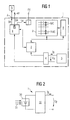
- Figure 1 shows a semiconductor chip 1, which here as an integrated Memory is running.
- the memory has a matrix Memory cell array 8 with normal memory cells MC and redundant memory cells RMC to replace faulty ones normal memory cells MC, each along Column lines and row lines are arranged.
- the Semiconductor chip 1 also has a self-test unit 2, also called BIST (Built-In-Self-Test), for generation of test information and to carry out a functional test the normal memory cells MC. For example Test patterns (so-called patterns) in the memory cell array 8 read in and compared with read out data.
- the self-test unit 2 checks the functionality of the normal Memory cells MC.
- the self-test unit 2 also generates the voltage levels of the control signals.
- the self-test unit 2 then carries out an analysis by which of the normal memory cells MC by which of the redundant RMC memory cells must be replaced. It takes place then a storage of the repair information.
- the memory chip 1 has electrically programmable ones Storage units 9, in which one by the self-test unit 2 determined repair result can be programmed can.
- the electrically programmable storage units 9 are designed, for example, as so-called electrical fuses, which is also programmable by the self-test unit 2 are.
- In the storage units 9 are, for example Addresses of faulty normal memory cells MC are saved. To replace faulty normal memory cells MC are corresponding redundant memory cells RMC by the Storage units 9 activated.
- an energy source 3 is provided to the semiconductor chip 1 an electrical power supply from a contactless supply Provides energy.
- the energy source 3 is in this embodiment arranged on the semiconductor chip 1.
- the Energy source 3 is with a voltage detector or current detector 6 connected to a characteristic voltage sequence or current sequence of the operating voltage UB or the operating current IB can detect.
- the voltage detector or Current detector 6 is connected to the self-test unit 2 Triggering a function test following a detected one characteristic voltage sequence or current sequence.
- the semiconductor chip 1 also has a functional unit 4 on that trained for contactless transmission of data DA is the information about the test execution and / or contain a test result.
- the functional unit 4 contains for example a semiconductor laser through which optical Radiation pulses 41 can be generated according to the data to be transferred DA.
- the optical radiation pulses 41 are received by a receiver 5 outside the semiconductor chip 1 receive.
- the functional unit 4 is with the self-test unit 2 connected.
- the functional unit 4 is still with connected to the voltage detector or current detector 6, which at Detection of a characteristic voltage sequence or Current sequence a data transmission through the functional unit 4 triggers.
- the functional unit 4 an output port A, for example in the form of a Connection pads, through which the data to be transmitted DA capacitive coupling to the receiver 5 are transmitted.
- receiver 5 has suitable test probes which are in a a sufficiently small distance to port A must be arranged.
- the semiconductor chip 1 also contains a non-volatile one Storage unit 7 for storing the data DA.
- the storage unit 7 is with a terminal EX of the semiconductor chip connected. For example, during the EX connection a block test the stored data DA of the storage unit 7 read out.
- FIG. 2 shows an embodiment of the test arrangement as electrical block diagram shown.
- the energy source 3 has a solar cell 30 through which an operating current IB on the semiconductor chip 1 by contactlessly supplied optical radiation 31 can be generated.
- a current limiter circuit 32 is provided for the solar cell 30, in the event of a limit being exceeded of the operating current IB the semiconductor chip 1 from the solar cell 30 separates. This is particularly advantageous if the Solar cell 30 as a common energy source for several to be tested Semiconductor chips is used. For example in the event of a short circuit, other semiconductor chips to be tested not affected because the faulty chip by the current limiter circuit 32 is disconnected from the power supply.
- FIG. 3 shows a further embodiment of the test arrangement shown.
- the semiconductor chip 1 has a material 42 that is irradiated with optical radiation 43.
- optical radiation 43 is the optical refraction of the optical radiation 43 by a potential UA controllable.
- Angle of refraction ⁇ of the refracted optical radiation 44 is outside of the receiver 5 of the semiconductor chip 1 received.
- the material 42 is connected to the connection A of the functional unit 4, on the the potential UA is present.
- This potential is corresponding of the data to be transferred DA controllable. That means the Refraction angle ⁇ is dependent on the one to be transmitted Data DA varies. This is how electrical stray fields on the Connection A through the potential UA present there by means of a electro-optical control exploited.
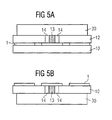
- FIG. 5a shows a cross section in a further embodiment an arrangement in which on a substrate or Semiconductor wafer 10 arranged several semiconductor chips 1 are.
- the solar cell 30 is all over the surface the semiconductor wafer 10 arranged.
- a radiation-absorbing Layer 12 applied between the solar cell 30 and the semiconductor wafer 10 is a radiation-absorbing Layer 12 applied. In the event that the solar cell 30 radiation down to the semiconductor wafer 10 transmits, is through the radiation-absorbing layer 12th generation of charge carriers on the semiconductor chips 1 is avoided.
- FIG. 5b shows an arrangement in a further embodiment, in which the solar cell 30 on the lower surface a substrate or the semiconductor wafer 10 is arranged, which faces away from the semiconductor chips 1.
- an electrical one conductive via 13 arranged in the substrate, by way of example on a single via 13 shown.
- a pn junction 14 along the via 13 arranged.
- the pn junction 14 is used for prevention a current flow between the via 13 and the Substrate.
- the via 13 and the pn junction 14 are similarly used for the same purpose in radiation-absorbing Layer 12 arranged according to Figure 5a. This can also be provided in the arrangement according to FIG. 5b become.
Landscapes
- Engineering & Computer Science (AREA)
- General Engineering & Computer Science (AREA)
- Physics & Mathematics (AREA)
- General Physics & Mathematics (AREA)
- Computer Networks & Wireless Communication (AREA)
- Testing Or Measuring Of Semiconductors Or The Like (AREA)
- For Increasing The Reliability Of Semiconductor Memories (AREA)
- Dram (AREA)
- Tests Of Electronic Circuits (AREA)
- Semiconductor Integrated Circuits (AREA)
Applications Claiming Priority (2)
| Application Number | Priority Date | Filing Date | Title |
|---|---|---|---|
| DE10016996A DE10016996C1 (de) | 2000-04-05 | 2000-04-05 | Testanordnung zur Funktionsprüfung eines Halbleiterchips |
| DE10016996 | 2000-04-05 |
Publications (3)
| Publication Number | Publication Date |
|---|---|
| EP1143256A2 true EP1143256A2 (fr) | 2001-10-10 |
| EP1143256A3 EP1143256A3 (fr) | 2003-11-12 |
| EP1143256B1 EP1143256B1 (fr) | 2005-01-26 |
Family
ID=7637718
Family Applications (1)
| Application Number | Title | Priority Date | Filing Date |
|---|---|---|---|
| EP01104945A Expired - Lifetime EP1143256B1 (fr) | 2000-04-05 | 2001-02-28 | Dispositif de test pour le test fonctionnel d'un circuit semiconducteur |
Country Status (6)
| Country | Link |
|---|---|
| US (1) | US6825682B2 (fr) |
| EP (1) | EP1143256B1 (fr) |
| JP (1) | JP3733298B2 (fr) |
| KR (1) | KR100397385B1 (fr) |
| DE (2) | DE10016996C1 (fr) |
| TW (1) | TW536631B (fr) |
Families Citing this family (20)
| Publication number | Priority date | Publication date | Assignee | Title |
|---|---|---|---|---|
| JP2003031666A (ja) * | 2001-07-12 | 2003-01-31 | Mitsubishi Electric Corp | 半導体デバイスまたは半導体ウェハ一括のテスト装置及びテスト方法 |
| EP1281603B1 (fr) | 2001-07-31 | 2005-11-02 | Nissan Motor Company Limited | Structure avant de véhicule automobile |
| KR100472460B1 (ko) * | 2002-07-04 | 2005-03-10 | 삼성전자주식회사 | 메모리의 결함 복구 방법 및 그에 적합한 장치 |
| TW559672B (en) * | 2002-07-24 | 2003-11-01 | Via Tech Inc | Testing method of chip configuration setup |
| US7030977B2 (en) * | 2003-05-06 | 2006-04-18 | Visteon Global Technologies, Inc. | Non-contact optical system for production testing of electronic assemblies |
| US7220990B2 (en) | 2003-08-25 | 2007-05-22 | Tau-Metrix, Inc. | Technique for evaluating a fabrication of a die and wafer |
| US7295480B2 (en) * | 2003-12-18 | 2007-11-13 | Agere Systems Inc | Semiconductor memory repair methodology using quasi-non-volatile memory |
| GB0329516D0 (en) * | 2003-12-19 | 2004-01-28 | Univ Kent Canterbury | Integrated circuit with debug support interface |
| KR101270180B1 (ko) * | 2004-01-30 | 2013-05-31 | 가부시키가이샤 한도오따이 에네루기 켄큐쇼 | 검사장치 및 검사방법과, 반도체장치 제작방법 |
| US7215133B2 (en) * | 2004-01-30 | 2007-05-08 | International Business Machines Corporation | Contactless circuit testing for adaptive wafer processing |
| US7466157B2 (en) * | 2004-02-05 | 2008-12-16 | Formfactor, Inc. | Contactless interfacing of test signals with a device under test |
| US20050210739A1 (en) * | 2004-03-09 | 2005-09-29 | Conocophillips Company | Blends of synthetic distillate and biodiesel for low nitrogen oxide emissions from diesel engines |
| CN100401490C (zh) * | 2004-07-09 | 2008-07-09 | 日月光半导体制造股份有限公司 | 重测半导体元件的方法 |
| US20060109120A1 (en) * | 2004-11-19 | 2006-05-25 | Jeremy Burr | RFID tag in a substrate |
| TWI316712B (en) * | 2006-06-27 | 2009-11-01 | Silicon Motion Inc | Non-volatile memory, repair circuit, and repair method thereof |
| KR100990942B1 (ko) * | 2008-08-29 | 2010-11-01 | 주식회사 하이닉스반도체 | 반도체 패키지용 기판 및 이를 갖는 반도체 패키지 |
| CN113539319B (zh) | 2020-04-21 | 2024-08-06 | 铁电存储器股份有限公司 | 存储单元电路、存储单元装置及其方法 |
| CN114089166A (zh) * | 2021-11-29 | 2022-02-25 | 江苏捷策创电子科技有限公司 | 一种芯片测试装置和方法 |
| KR20230085632A (ko) | 2021-12-07 | 2023-06-14 | 에스케이하이닉스 주식회사 | 저장 장치, 호스트 장치 및 이들을 포함하는 컴퓨팅 시스템 |
| JP7495764B1 (ja) | 2023-04-04 | 2024-06-05 | 株式会社M3 | 非接触検査機能を備える半導体ウェハ |
Family Cites Families (19)
| Publication number | Priority date | Publication date | Assignee | Title |
|---|---|---|---|---|
| JPS58182444A (ja) | 1982-04-16 | 1983-10-25 | Mitsubishi Electric Corp | 水封式電動機の固定子巻線の結束方法 |
| JPH02110339A (ja) | 1988-10-19 | 1990-04-23 | Fujikura Ltd | プリント基板製造におけるテンティング強度測定方法 |
| US5270655A (en) * | 1989-12-22 | 1993-12-14 | Matsushita Electric Industrial Co., Ltd. | Semiconductor integrated circuit having light emitting devices |
| US5130645A (en) * | 1990-08-13 | 1992-07-14 | Vlsi Technology, Inc. | Integrated circuit built-in self-test structure |
| JP2937471B2 (ja) | 1990-11-29 | 1999-08-23 | 株式会社日立製作所 | 半導体集積回路 |
| US5274336A (en) | 1992-01-14 | 1993-12-28 | Hewlett-Packard Company | Capacitively-coupled test probe |
| US5313424A (en) | 1992-03-17 | 1994-05-17 | International Business Machines Corporation | Module level electronic redundancy |
| US5241266A (en) * | 1992-04-10 | 1993-08-31 | Micron Technology, Inc. | Built-in test circuit connection for wafer level burnin and testing of individual dies |
| US6058497A (en) * | 1992-11-20 | 2000-05-02 | Micron Technology, Inc. | Testing and burn-in of IC chips using radio frequency transmission |
| US5570035A (en) * | 1995-01-31 | 1996-10-29 | The United States Of America As Represented By The Secretary Of The Army | Built-in self test indicator for an integrated circuit package |
| US6087842A (en) * | 1996-04-29 | 2000-07-11 | Agilent Technologies | Integrated or intrapackage capability for testing electrical continuity between an integrated circuit and other circuitry |
| US5764655A (en) * | 1997-07-02 | 1998-06-09 | International Business Machines Corporation | Built in self test with memory |
| JPH1168209A (ja) | 1997-08-11 | 1999-03-09 | Ishikawajima Harima Heavy Ind Co Ltd | 電界制御による波長可変マイクロチップレーザ |
| WO1999032893A1 (fr) * | 1997-12-22 | 1999-07-01 | Conexant Systems, Inc. | Dispositif d'essai sans fil pour microplaquette |
| US6119255A (en) * | 1998-01-21 | 2000-09-12 | Micron Technology, Inc. | Testing system for evaluating integrated circuits, a burn-in testing system, and a method for testing an integrated circuit |
| US6331782B1 (en) * | 1998-03-23 | 2001-12-18 | Conexant Systems, Inc. | Method and apparatus for wireless testing of integrated circuits |
| JP2000048131A (ja) | 1998-07-29 | 2000-02-18 | Hitachi Ltd | Icカードの試験方法および装置 |
| US6300785B1 (en) * | 1998-10-20 | 2001-10-09 | International Business Machines Corporation | Contact-less probe of semiconductor wafers |
| JP2000188311A (ja) | 1998-12-24 | 2000-07-04 | Sharp Corp | 集積回路装置の自己テスト方法 |
-
2000
- 2000-04-05 DE DE10016996A patent/DE10016996C1/de not_active Expired - Fee Related
-
2001
- 2001-02-28 EP EP01104945A patent/EP1143256B1/fr not_active Expired - Lifetime
- 2001-02-28 DE DE50105163T patent/DE50105163D1/de not_active Expired - Fee Related
- 2001-03-27 TW TW090107193A patent/TW536631B/zh not_active IP Right Cessation
- 2001-04-04 KR KR10-2001-0017980A patent/KR100397385B1/ko not_active Expired - Fee Related
- 2001-04-05 US US09/826,594 patent/US6825682B2/en not_active Expired - Fee Related
- 2001-04-05 JP JP2001107638A patent/JP3733298B2/ja not_active Expired - Fee Related
Also Published As
| Publication number | Publication date |
|---|---|
| KR100397385B1 (ko) | 2003-09-17 |
| DE10016996C1 (de) | 2002-02-07 |
| US6825682B2 (en) | 2004-11-30 |
| JP2001357698A (ja) | 2001-12-26 |
| DE50105163D1 (de) | 2005-03-03 |
| EP1143256A3 (fr) | 2003-11-12 |
| EP1143256B1 (fr) | 2005-01-26 |
| KR20010095326A (ko) | 2001-11-03 |
| TW536631B (en) | 2003-06-11 |
| US20010043078A1 (en) | 2001-11-22 |
| JP3733298B2 (ja) | 2006-01-11 |
Similar Documents
| Publication | Publication Date | Title |
|---|---|---|
| EP1143256B1 (fr) | Dispositif de test pour le test fonctionnel d'un circuit semiconducteur | |
| EP0212208B1 (fr) | Méthode pour tester des éléments d'un circuit intégré | |
| DE3888395T2 (de) | Prüfungssystem für eine Mikrokreisanordnung mit Redundanzkreisanlagen. | |
| DE69808956T2 (de) | Teilweise abschaltbare spannungsversorgung für integrierte schaltkreise | |
| DE3851847T2 (de) | Integrierte Halbleiterschaltung mit einer Mehrzahl von Schaltungsblöcken äquivalenter Funktionen. | |
| DE69426817T2 (de) | Fertigungprüfungsverfahren von Flash-EEPROM-Vorrichtungen | |
| DE112019001445T5 (de) | Gezielter rückruf von halbleiterbauelementen aufgrund von herstellungsdaten | |
| DE69523009T2 (de) | Schaltungsstruktur und Verfahren zur Belastungsprüfung von Bitleitungen | |
| DE102008021640A1 (de) | Schaltung und Verfahren zum Finden von Wortleitung-Bitleitung-Kurzschlüssen in einem DRAM | |
| DE10162222A1 (de) | Optische Testanordnung und Verfahren | |
| DE19801557B4 (de) | Kontakt-Prüfschaltung in einer Halbleitereinrichtung | |
| DE102008031288A1 (de) | Speichervorrichtung und Verfahren zum Testen einer Speichervorrichtung | |
| DE69030168T2 (de) | Schaltung zum Einbringen von Identifizierungsinformation auf einer Schaltungsmikroplatte | |
| DE102022108486A1 (de) | Optisches Prüfsystem und optisches Prüfverfahren | |
| EP0843317B1 (fr) | Méthode de test d'une puce de mémoire divisé en champs de cellules pendant le fonctionnement de l'ordinateur en maintenant des conditions de temps réel | |
| WO2005052612A2 (fr) | Circuit d'entree et de sortie d'un circuit de commutation integre, procede pour tester un circuit de commutation integre et circuit de commutation integre dote d'un circuit d'entree et de sortie de ce type | |
| DE68910322T2 (de) | Verfahren zur Inspektion von Durchkontakt-Stiften in integrierten Schaltungspackungen mittels Photoemission. | |
| DE69516768T2 (de) | Prüfbarer i ddq- speicher durch kumulative wort-zeilen-aktivierung | |
| DE4312238C2 (de) | Verfahren zum Befreien einer Halbleiterspeichervorrichtung von einem Kurzschluß | |
| DE69504072T2 (de) | Speicherprüfsystem | |
| DE68922381T2 (de) | Überwachungsstruktur für Dünnschichtverdrahtungen. | |
| EP1416288B1 (fr) | Procédé et dispositif de détection optique des défauts mécaniques dans des dispositifs à semi-conducteur, notamment pour systèmes de cellules solaires | |
| EP0945804B1 (fr) | Circuit intégré et son procédé de test | |
| DE69420214T2 (de) | Optischer Abtastkopf und optischer Detektor dafür | |
| EP0891623A1 (fr) | Montage avec circuit de test |
Legal Events
| Date | Code | Title | Description |
|---|---|---|---|
| PUAI | Public reference made under article 153(3) epc to a published international application that has entered the european phase |
Free format text: ORIGINAL CODE: 0009012 |
|
| AK | Designated contracting states |
Kind code of ref document: A2 Designated state(s): AT BE CH CY DE DK ES FI FR GB GR IE IT LI LU MC NL PT SE TR |
|
| AX | Request for extension of the european patent |
Free format text: AL;LT;LV;MK;RO;SI |
|
| PUAL | Search report despatched |
Free format text: ORIGINAL CODE: 0009013 |
|
| AK | Designated contracting states |
Kind code of ref document: A3 Designated state(s): AT BE CH CY DE DK ES FI FR GB GR IE IT LI LU MC NL PT SE TR |
|
| AX | Request for extension of the european patent |
Extension state: AL LT LV MK RO SI |
|
| 17P | Request for examination filed |
Effective date: 20040511 |
|
| GRAP | Despatch of communication of intention to grant a patent |
Free format text: ORIGINAL CODE: EPIDOSNIGR1 |
|
| AKX | Designation fees paid |
Designated state(s): DE FR GB IE IT |
|
| GRAS | Grant fee paid |
Free format text: ORIGINAL CODE: EPIDOSNIGR3 |
|
| GRAA | (expected) grant |
Free format text: ORIGINAL CODE: 0009210 |
|
| AK | Designated contracting states |
Kind code of ref document: B1 Designated state(s): DE FR GB IE IT |
|
| REG | Reference to a national code |
Ref country code: GB Ref legal event code: FG4D Free format text: NOT ENGLISH |
|
| REG | Reference to a national code |
Ref country code: IE Ref legal event code: FG4D Free format text: GERMAN |
|
| REF | Corresponds to: |
Ref document number: 50105163 Country of ref document: DE Date of ref document: 20050303 Kind code of ref document: P |
|
| GBT | Gb: translation of ep patent filed (gb section 77(6)(a)/1977) |
Effective date: 20050420 |
|
| PLBE | No opposition filed within time limit |
Free format text: ORIGINAL CODE: 0009261 |
|
| STAA | Information on the status of an ep patent application or granted ep patent |
Free format text: STATUS: NO OPPOSITION FILED WITHIN TIME LIMIT |
|
| ET | Fr: translation filed | ||
| 26N | No opposition filed |
Effective date: 20051027 |
|
| PGFP | Annual fee paid to national office [announced via postgrant information from national office to epo] |
Ref country code: GB Payment date: 20070216 Year of fee payment: 7 |
|
| PGFP | Annual fee paid to national office [announced via postgrant information from national office to epo] |
Ref country code: IE Payment date: 20080220 Year of fee payment: 8 Ref country code: IT Payment date: 20080223 Year of fee payment: 8 |
|
| PGFP | Annual fee paid to national office [announced via postgrant information from national office to epo] |
Ref country code: DE Payment date: 20080415 Year of fee payment: 8 Ref country code: FR Payment date: 20080214 Year of fee payment: 8 |
|
| GBPC | Gb: european patent ceased through non-payment of renewal fee |
Effective date: 20080228 |
|
| PG25 | Lapsed in a contracting state [announced via postgrant information from national office to epo] |
Ref country code: GB Free format text: LAPSE BECAUSE OF NON-PAYMENT OF DUE FEES Effective date: 20080228 |
|
| REG | Reference to a national code |
Ref country code: FR Ref legal event code: ST Effective date: 20091030 |
|
| REG | Reference to a national code |
Ref country code: IE Ref legal event code: MM4A |
|
| PG25 | Lapsed in a contracting state [announced via postgrant information from national office to epo] |
Ref country code: IE Free format text: LAPSE BECAUSE OF NON-PAYMENT OF DUE FEES Effective date: 20090302 Ref country code: DE Free format text: LAPSE BECAUSE OF NON-PAYMENT OF DUE FEES Effective date: 20090901 |
|
| PG25 | Lapsed in a contracting state [announced via postgrant information from national office to epo] |
Ref country code: FR Free format text: LAPSE BECAUSE OF NON-PAYMENT OF DUE FEES Effective date: 20090302 |
|
| PG25 | Lapsed in a contracting state [announced via postgrant information from national office to epo] |
Ref country code: IT Free format text: LAPSE BECAUSE OF NON-PAYMENT OF DUE FEES Effective date: 20090228 |