EP1143459A2 - Méthode de fabrication successif de fils conducteurs minces et carrés - Google Patents
Méthode de fabrication successif de fils conducteurs minces et carrés Download PDFInfo
- Publication number
- EP1143459A2 EP1143459A2 EP01250056A EP01250056A EP1143459A2 EP 1143459 A2 EP1143459 A2 EP 1143459A2 EP 01250056 A EP01250056 A EP 01250056A EP 01250056 A EP01250056 A EP 01250056A EP 1143459 A2 EP1143459 A2 EP 1143459A2
- Authority
- EP
- European Patent Office
- Prior art keywords
- square
- conductive wire
- material sheet
- square conductive
- cutting
- Prior art date
- Legal status (The legal status is an assumption and is not a legal conclusion. Google has not performed a legal analysis and makes no representation as to the accuracy of the status listed.)
- Withdrawn
Links
Images

Classifications
-
- H—ELECTRICITY
- H01—ELECTRIC ELEMENTS
- H01B—CABLES; CONDUCTORS; INSULATORS; SELECTION OF MATERIALS FOR THEIR CONDUCTIVE, INSULATING OR DIELECTRIC PROPERTIES
- H01B13/00—Apparatus or processes specially adapted for manufacturing conductors or cables
-
- Y—GENERAL TAGGING OF NEW TECHNOLOGICAL DEVELOPMENTS; GENERAL TAGGING OF CROSS-SECTIONAL TECHNOLOGIES SPANNING OVER SEVERAL SECTIONS OF THE IPC; TECHNICAL SUBJECTS COVERED BY FORMER USPC CROSS-REFERENCE ART COLLECTIONS [XRACs] AND DIGESTS
- Y10—TECHNICAL SUBJECTS COVERED BY FORMER USPC
- Y10T—TECHNICAL SUBJECTS COVERED BY FORMER US CLASSIFICATION
- Y10T83/00—Cutting
- Y10T83/04—Processes
- Y10T83/0524—Plural cutting steps
- Y10T83/0538—Repetitive transverse severing from leading edge of work
- Y10T83/0548—With longitudinal severing
Definitions
- This Invention relates to a method of successively manufacturing slender square conductive wires having a square cross section.
- the coil in order to implement these means within a limited space such as that of a coil bobbin, the coil must be caused to have an increased sectional area and must be wound as dense as possible.
- a large-sized rectangular or square conductive wire has been used as a coil for a synchrotron, magnetic field generating device for superconducting or a large-scale transformer.
- the large-sized rectangular or square conductive wire is molded by a known roll diffusion or die cutting.
- the molded rectangular or square conductive wire thus manufactured has an "R" at its corners generated by the above technique. This is not problematic because the conductive wire is large-sized or thick.
- the square conductive wire having a relatively small size manufactured by the above technique involves the "R" at the corner which is large relatively to the size of the square conductive wire.
- the square conductive wire having a size having 1 x 1 mm or less, which involves a large "R" could not be made in a desired shape.
- slice cutting systems In order to create a rectangular shape with no "R" or deformation at the corner of the square conductive wire, slice cutting systems have been widely used in a process of manufacturing many industrial products. However, most of the slice cutting systems, which have a large width, could not be applied to the square conductive wire having a desired size.
- An object of this invention is to provide a method of successively manufacturing a square conductive wire having a small size.
- a method of manufacturing a square conductive wire which has a square-shape with four equal sides in section, comprising the steps of:
- a slender square conductive wire which is a square in section can be obtained. More specifically, by cutting a very thin conductive material sheet at intervals each being equal to the length of the each the sides in a direction orthogonal to the front and the rear surface thereof, a slender square conducive conductive wire which is a square with greatly reduced sides in section can be manufactured. Using the conductive material sheet having a more reduced thickness, a more slender, or more small-sized square conductive wire can be obtained. Further, by lengthening the conductive material sheet, the square conductive wires can be obtained successively.
- small-sized square conductive wires can be obtained successively.
- the square conductive wire manufactured by this invention has the following advantages as compared with a round conductive wire which is round in section.
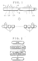
- Fig. 1 is a view showing an embodiment of a method of manufacturing a square conductive wire according to this invention
- Fig. 2 is a flowchart for explaining the method of manufacturing a square conductive wire.
- a square conductive wire 1 with four sides each having a length T in its section is made by cutting a material sheet 2 with a thickness T to provide a width T.
- the thickness of the material sheet 2 is preferably selected on the basis of the standard of a conductor diameter for "appendix 6: polyurethane" of "JIS C 3202 ENAMEL WIRE".
- the material sheet which is extremely thin is selected.
- the square conductive wire 1 is manufactured from the material sheet 2 which is extremely thin.
- the method of manufacturing the square conductive wire 1 having a size of T x T mm comprises the steps of preparing a material sheet 2 (step S1) and cutting the material sheet 2 to obtain the square conductive wire (step S2).
- the material sheet 2 is prepared as a very thin plate made of a conductive metallic material (e.g. aluminum and copper) having a thickness of T.
- the material sheet 2 has a front surface 3 and a rear surface which are in parallel to each other.
- the material sheet 2 has a length required for the square wire 1.
- step S2 the material sheet 2 thus prepared is cut at the respective positions of wires L1 to Ln.
- the wires L1 to Ln are arranged in parallel at intervals T.
- the direction of the wires L1 to Ln are orthogonal to the front surface 3 and rear surface 4.
- the material sheet 2 can be cut by various cutting tools as described below.
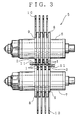
- the cutting tool is built in an apparatus for manufacturing the square conductive wire 1. Referring to Figs. 3 to 5, three examples of the cutting tool will be explained.
- Fig. 3 shows a first example of the cutting tool.
- a cutting portion 5 in the above manufacturing apparatus serves as the cutting tool. More specifically, the cutting portion 5 includes an upper axis cutter roller 6 and a lower axis cutter roller 7 which are individually rolled by a servo motor (not shown).
- the upper axis cutter roller 6 and lower axis cutter roller 7 each has a plurality of disk-shaped cutters at its intermediate portion. The thickness of the cutter is equal to the thickness T of the material sheet 2 (Fig. 1).
- the cutters of the upper axis cutter roller 6 and those of the lower axis cutter roller 7. are arranged in a staggered configuration.
- spacers 9 each having a smaller diameter than that of the cutter 8 are arranged.
- Rings 10 each is provided to be kept in contact with the outer edge of the spacer 9.
- the rings 10 each has a sufficiently larger radius of curvature than that of the cutter 8.
- the axis center of the ring 10 is located outside of that of the cutter 8.
- the space 9 has a thickness which is slightly larger than the thickness T of the material sheet 2 (Fig. 1).
- the ring 10 has a thickness which is slightly smaller than the thickness T of the material sheet 2 (Fig. 1).
- the material sheet 2 is fed to between these cutter rollers 6 and 7. Then, the material sheet 2 is cut successively so as to provide a thickness of T by the respective cutters (Fig. 1). In this case, the material sheet 2 will be cut in a direction orthogonal to the front and the rear surface thereof. In accordance with this example, the material sheet 2 thus cut is divided into six square conductive wires and two end members 11 which are a yield.
- Fig. 4 shows a second example of the cutting tool.
- a cutting portion 12 in the above manufacturing apparatus serves as the cutting tool.
- the cutting portion 12 includes a laser oscillator 13.
- the laser oscillator 13 has a plurality of laser heads 14 arranged by a suitable means.
- Optical fibers 15 integrally couple the laser oscillator 13 and the laser heads 14 with each other.
- the material sheet 2 fed to the cutting portion 12 is cut at intervals of width T by means of the laser oscillator 13.
- the square conductive wire 1 (Fig. 1) is obtained.
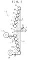
- Fig. 4 shows a third example of the cutting tool.
- a cutting portion 16 in the above manufacturing apparatus serves as the cutting tool. More specifically, the cutting portion 16 includes a wire 17.
- the wire 17 under tension is supplied from a reel 18 and taken up by a reel 19.
- the wire 17 is stretched at intervals of T in a direction orthogonal to the front surface and the rear surface of the material sheet 2.
- reference numeral 20 denotes a member for direction-inverting for the wire 17.
- Reference numeral 21 is a nozzle for scattering abrasive and cutting oil.
- the material sheet 2 fed to the cutting portion 16 is cut at intervals of width T by the wire.
- the square conductive wires 1 (Fig. 1) can be obtained.
- the small-sized or slender square conductive wires can be manufactured successively.
- the small-sized conductive wire which could not be manufactured by the known roll diffusion bonding and die cutting technique can be manufactured by the manufacturing method according to this invention.
Landscapes
- Engineering & Computer Science (AREA)
- Manufacturing & Machinery (AREA)
- Wire Processing (AREA)
- Shearing Machines (AREA)
- Finish Polishing, Edge Sharpening, And Grinding By Specific Grinding Devices (AREA)
- Non-Insulated Conductors (AREA)
Applications Claiming Priority (2)
| Application Number | Priority Date | Filing Date | Title |
|---|---|---|---|
| JP2000106168A JP3523561B2 (ja) | 2000-04-07 | 2000-04-07 | 真四角線の製造方法 |
| JP2000106168 | 2000-04-07 |
Publications (2)
| Publication Number | Publication Date |
|---|---|
| EP1143459A2 true EP1143459A2 (fr) | 2001-10-10 |
| EP1143459A3 EP1143459A3 (fr) | 2002-11-20 |
Family
ID=18619391
Family Applications (1)
| Application Number | Title | Priority Date | Filing Date |
|---|---|---|---|
| EP01250056A Withdrawn EP1143459A3 (fr) | 2000-04-07 | 2001-02-22 | Méthode de fabrication successif de fils conducteurs minces et carrés |
Country Status (3)
| Country | Link |
|---|---|
| US (2) | US20010027707A1 (fr) |
| EP (1) | EP1143459A3 (fr) |
| JP (1) | JP3523561B2 (fr) |
Cited By (1)
| Publication number | Priority date | Publication date | Assignee | Title |
|---|---|---|---|---|
| WO2021118500A1 (fr) * | 2019-12-09 | 2021-06-17 | Orta Dogu Teknik Universitesi | Procédé d'enroulement pour machines électriques |
Families Citing this family (3)
| Publication number | Priority date | Publication date | Assignee | Title |
|---|---|---|---|---|
| JP5421064B2 (ja) | 2009-10-26 | 2014-02-19 | 後藤電子 株式会社 | 高周波高圧高電流電線 |
| WO2013168262A1 (fr) * | 2012-05-10 | 2013-11-14 | トヨタ自動車株式会社 | Faisceau de câbles et méthode de fabrication de celui-ci |
| JP7729306B2 (ja) * | 2022-10-11 | 2025-08-26 | 株式会社村田製作所 | インダクタ |
Family Cites Families (14)
| Publication number | Priority date | Publication date | Assignee | Title |
|---|---|---|---|---|
| US281184A (en) * | 1883-07-10 | Roll for slitting iron | ||
| US87557A (en) * | 1869-03-09 | Thaddeus fowler | ||
| US1738828A (en) * | 1925-03-02 | 1929-12-10 | Jackson Arthur Hews | Low-resistance permanent wire |
| US2075906A (en) * | 1932-04-06 | 1937-04-06 | Aylmer H Maude | Conductor |
| US3543205A (en) * | 1968-08-05 | 1970-11-24 | Westinghouse Electric Corp | Electrical windings |
| US3842193A (en) * | 1973-07-06 | 1974-10-15 | Anaconda Co | Glass insulated magnet wire |
| US4011109A (en) * | 1975-11-10 | 1977-03-08 | Monsanto Company | Method for producing steel filaments |
| US4275491A (en) * | 1977-02-08 | 1981-06-30 | Roberto Marinucci | Multi-complex shear device for splitting hot metallic bars into several smaller bars |
| US6123788A (en) * | 1993-04-19 | 2000-09-26 | Electrocopper Products Limited | Copper wire and process for making copper wire |
| JPH076637A (ja) * | 1993-06-16 | 1995-01-10 | Sumitomo Electric Ind Ltd | テープ状電線の製造方法 |
| JP3598581B2 (ja) * | 1995-05-19 | 2004-12-08 | 株式会社デンソー | 発電機の回転子コイルおよびその製造方法 |
| IT1288842B1 (it) * | 1996-01-26 | 1998-09-25 | Simac Spa | Metodo e rispettivo impianto di laminazione a caldo per la produzione in continuo di barre, tondini o filo |
| US6179988B1 (en) * | 1997-08-29 | 2001-01-30 | Electrocopper Products Limited | Process for making copper wire |
| FR2780545B1 (fr) * | 1998-06-30 | 2000-08-25 | Siemens Automotive Sa | Procede et dispositif de fabrication de faisceaux de cables plats |
-
2000
- 2000-04-07 JP JP2000106168A patent/JP3523561B2/ja not_active Expired - Fee Related
-
2001
- 2001-02-22 US US09/789,414 patent/US20010027707A1/en not_active Abandoned
- 2001-02-22 EP EP01250056A patent/EP1143459A3/fr not_active Withdrawn
-
2003
- 2003-03-13 US US10/388,299 patent/US20030159557A1/en not_active Abandoned
Cited By (1)
| Publication number | Priority date | Publication date | Assignee | Title |
|---|---|---|---|---|
| WO2021118500A1 (fr) * | 2019-12-09 | 2021-06-17 | Orta Dogu Teknik Universitesi | Procédé d'enroulement pour machines électriques |
Also Published As
| Publication number | Publication date |
|---|---|
| US20030159557A1 (en) | 2003-08-28 |
| JP3523561B2 (ja) | 2004-04-26 |
| EP1143459A3 (fr) | 2002-11-20 |
| JP2001291444A (ja) | 2001-10-19 |
| US20010027707A1 (en) | 2001-10-11 |
Similar Documents
| Publication | Publication Date | Title |
|---|---|---|
| GB1561032A (en) | Laminated foil stator | |
| CN87105579A (zh) | 创造磁心的方法 | |
| EP0269347A2 (fr) | Noyau enroulé dont la section présente une périphérie ayant des portions circulaires et elliptiques | |
| EP1143459A2 (fr) | Méthode de fabrication successif de fils conducteurs minces et carrés | |
| US20050013025A1 (en) | Optical filter, production method for this optical filter and optical device using this optical filter and housing structure for this optical filter | |
| JPH0576259B2 (fr) | ||
| EP0362035B1 (fr) | Procédé et dispositif pour découper des bandes pour des noyaux enroulés | |
| EP0618660B1 (fr) | Procédure de fabrication du stator d'un moteur pas-à-pas | |
| HK1000296B (en) | Method of cutting strips for wound core, and apparatus therefore | |
| KR102314493B1 (ko) | 표면이 가공된 초전도선재 및 그 제조방법 | |
| US11843289B2 (en) | Method for manufacturing a core element for an electric machine | |
| JP2002075747A (ja) | ギャップ付磁芯およびその製造方法 | |
| JP2002307104A (ja) | 四角線の製造装置及び製造方法 | |
| US4854035A (en) | Method of manufacturing a magnetic head | |
| JP2001287115A (ja) | 真四角線の製造装置 | |
| JPH0456304A (ja) | 積層形コアの製造方法 | |
| JPS58186514A (ja) | 面取付きスリツト法 | |
| JP2959175B2 (ja) | 台形コイルの製造方法 | |
| JP2004087668A (ja) | 鉄心及びこれを用いたコイル装置並びにこれらの製造方法 | |
| JPS599974B2 (ja) | 磁気ヘツドの製造方法 | |
| JPS6120361A (ja) | 半導体装置用リ−ドフレ−ムの製造方法 | |
| JP2607477B2 (ja) | ステッピングモータのヨークの成形方法 | |
| JPH0439734B2 (fr) | ||
| JP2021191078A (ja) | アキシャルギャップモータ用ステータ及びその製造方法並びにアキシャルギャップモータ | |
| JP3113598B2 (ja) | 銅合金条材の取出し方法 |
Legal Events
| Date | Code | Title | Description |
|---|---|---|---|
| PUAI | Public reference made under article 153(3) epc to a published international application that has entered the european phase |
Free format text: ORIGINAL CODE: 0009012 |
|
| AK | Designated contracting states |
Kind code of ref document: A2 Designated state(s): AT BE CH CY DE DK ES FI FR GB GR IE IT LI LU MC NL PT SE TR |
|
| AX | Request for extension of the european patent |
Free format text: AL;LT;LV;MK;RO;SI |
|
| PUAL | Search report despatched |
Free format text: ORIGINAL CODE: 0009013 |
|
| AK | Designated contracting states |
Kind code of ref document: A3 Designated state(s): AT BE CH CY DE DK ES FI FR GB GR IE IT LI LU MC NL PT SE TR |
|
| AX | Request for extension of the european patent |
Free format text: AL;LT;LV;MK;RO;SI |
|
| 17P | Request for examination filed |
Effective date: 20030128 |
|
| AKX | Designation fees paid |
Designated state(s): DE FR GB |
|
| 17Q | First examination report despatched |
Effective date: 20070312 |
|
| STAA | Information on the status of an ep patent application or granted ep patent |
Free format text: STATUS: THE APPLICATION IS DEEMED TO BE WITHDRAWN |
|
| 18D | Application deemed to be withdrawn |
Effective date: 20070724 |