EP1143506A2 - Procédé pour la fabrication d'un motif - Google Patents
Procédé pour la fabrication d'un motif Download PDFInfo
- Publication number
- EP1143506A2 EP1143506A2 EP01108301A EP01108301A EP1143506A2 EP 1143506 A2 EP1143506 A2 EP 1143506A2 EP 01108301 A EP01108301 A EP 01108301A EP 01108301 A EP01108301 A EP 01108301A EP 1143506 A2 EP1143506 A2 EP 1143506A2
- Authority
- EP
- European Patent Office
- Prior art keywords
- recess
- pattern
- film
- interlayer dielectric
- polishing
- Prior art date
- Legal status (The legal status is an assumption and is not a legal conclusion. Google has not performed a legal analysis and makes no representation as to the accuracy of the status listed.)
- Ceased
Links
Images


Classifications
-
- H—ELECTRICITY
- H10—SEMICONDUCTOR DEVICES; ELECTRIC SOLID-STATE DEVICES NOT OTHERWISE PROVIDED FOR
- H10P—GENERIC PROCESSES OR APPARATUS FOR THE MANUFACTURE OR TREATMENT OF DEVICES COVERED BY CLASS H10
- H10P52/00—Grinding, lapping or polishing of wafers, substrates or parts of devices
-
- H—ELECTRICITY
- H10—SEMICONDUCTOR DEVICES; ELECTRIC SOLID-STATE DEVICES NOT OTHERWISE PROVIDED FOR
- H10W—GENERIC PACKAGES, INTERCONNECTIONS, CONNECTORS OR OTHER CONSTRUCTIONAL DETAILS OF DEVICES COVERED BY CLASS H10
- H10W20/00—Interconnections in chips, wafers or substrates
- H10W20/01—Manufacture or treatment
- H10W20/031—Manufacture or treatment of conductive parts of the interconnections
- H10W20/062—Manufacture or treatment of conductive parts of the interconnections by smoothing of conductive parts, e.g. by planarisation
-
- H—ELECTRICITY
- H10—SEMICONDUCTOR DEVICES; ELECTRIC SOLID-STATE DEVICES NOT OTHERWISE PROVIDED FOR
- H10W—GENERIC PACKAGES, INTERCONNECTIONS, CONNECTORS OR OTHER CONSTRUCTIONAL DETAILS OF DEVICES COVERED BY CLASS H10
- H10W20/00—Interconnections in chips, wafers or substrates
- H10W20/01—Manufacture or treatment
- H10W20/031—Manufacture or treatment of conductive parts of the interconnections
- H10W20/056—Manufacture or treatment of conductive parts of the interconnections by filling conductive material into holes, grooves or trenches
- H10W20/057—Manufacture or treatment of conductive parts of the interconnections by filling conductive material into holes, grooves or trenches by selectively depositing, e.g. by using selective CVD or plating
-
- H—ELECTRICITY
- H10—SEMICONDUCTOR DEVICES; ELECTRIC SOLID-STATE DEVICES NOT OTHERWISE PROVIDED FOR
- H10W—GENERIC PACKAGES, INTERCONNECTIONS, CONNECTORS OR OTHER CONSTRUCTIONAL DETAILS OF DEVICES COVERED BY CLASS H10
- H10W20/00—Interconnections in chips, wafers or substrates
- H10W20/01—Manufacture or treatment
- H10W20/071—Manufacture or treatment of dielectric parts thereof
- H10W20/072—Manufacture or treatment of dielectric parts thereof of dielectric parts comprising air gaps
-
- H—ELECTRICITY
- H10—SEMICONDUCTOR DEVICES; ELECTRIC SOLID-STATE DEVICES NOT OTHERWISE PROVIDED FOR
- H10W—GENERIC PACKAGES, INTERCONNECTIONS, CONNECTORS OR OTHER CONSTRUCTIONAL DETAILS OF DEVICES COVERED BY CLASS H10
- H10W20/00—Interconnections in chips, wafers or substrates
- H10W20/01—Manufacture or treatment
- H10W20/071—Manufacture or treatment of dielectric parts thereof
- H10W20/092—Manufacture or treatment of dielectric parts thereof by smoothing the dielectric parts
-
- H—ELECTRICITY
- H10—SEMICONDUCTOR DEVICES; ELECTRIC SOLID-STATE DEVICES NOT OTHERWISE PROVIDED FOR
- H10W—GENERIC PACKAGES, INTERCONNECTIONS, CONNECTORS OR OTHER CONSTRUCTIONAL DETAILS OF DEVICES COVERED BY CLASS H10
- H10W20/00—Interconnections in chips, wafers or substrates
- H10W20/40—Interconnections external to wafers or substrates, e.g. back-end-of-line [BEOL] metallisations or vias connecting to gate electrodes
- H10W20/45—Interconnections external to wafers or substrates, e.g. back-end-of-line [BEOL] metallisations or vias connecting to gate electrodes characterised by their insulating parts
- H10W20/46—Interconnections external to wafers or substrates, e.g. back-end-of-line [BEOL] metallisations or vias connecting to gate electrodes characterised by their insulating parts comprising air gaps
-
- H—ELECTRICITY
- H10—SEMICONDUCTOR DEVICES; ELECTRIC SOLID-STATE DEVICES NOT OTHERWISE PROVIDED FOR
- H10P—GENERIC PROCESSES OR APPARATUS FOR THE MANUFACTURE OR TREATMENT OF DEVICES COVERED BY CLASS H10
- H10P52/00—Grinding, lapping or polishing of wafers, substrates or parts of devices
- H10P52/40—Chemomechanical polishing [CMP]
- H10P52/403—Chemomechanical polishing [CMP] of conductive or resistive materials
Definitions
- a polyimide resin film 404 is formed on the interlayer film 402 including the interiors of the trenches 403a and 403b, so the trenches 403a and 403b are filled with polyimide resin.
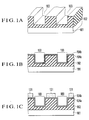
- planarization polishing in accordance with CMP described above, a slurry made of alumina is used. With this CMP, the projecting portions of the patterns 205a and 205b above the interlayer film 202 can be polished within about 3 min.
- the polishing end point may be set to a time point when it can be visually confirmed that the surface of the interlayer dielectric film 202 except the portions in the trenches 203a and 203b is exposed. With this polishing by CMP, once the surface of the interlayer dielectric film 202 made of silicon is exposed, progress of polishing becomes very slow, and the end point can be detected easily.
Landscapes
- Internal Circuitry In Semiconductor Integrated Circuit Devices (AREA)
- Mechanical Treatment Of Semiconductor (AREA)
- Weting (AREA)
- Polishing Bodies And Polishing Tools (AREA)
Applications Claiming Priority (4)
| Application Number | Priority Date | Filing Date | Title |
|---|---|---|---|
| JP2000102290 | 2000-04-04 | ||
| JP2000102296A JP3893009B2 (ja) | 2000-04-04 | 2000-04-04 | パターン形成方法 |
| JP2000102290 | 2000-04-04 | ||
| JP2000102296 | 2000-04-04 |
Publications (2)
| Publication Number | Publication Date |
|---|---|
| EP1143506A2 true EP1143506A2 (fr) | 2001-10-10 |
| EP1143506A3 EP1143506A3 (fr) | 2004-02-25 |
Family
ID=26589437
Family Applications (1)
| Application Number | Title | Priority Date | Filing Date |
|---|---|---|---|
| EP01108301A Ceased EP1143506A3 (fr) | 2000-04-04 | 2001-04-02 | Procédé pour la fabrication d'un motif |
Country Status (3)
| Country | Link |
|---|---|
| US (1) | US6468895B2 (fr) |
| EP (1) | EP1143506A3 (fr) |
| KR (1) | KR100424400B1 (fr) |
Cited By (2)
| Publication number | Priority date | Publication date | Assignee | Title |
|---|---|---|---|---|
| CN102358613A (zh) * | 2011-10-12 | 2012-02-22 | 中国电子科技集团公司第二十四研究所 | 一种mems拱形结构的制造方法 |
| CN103426814A (zh) * | 2012-05-24 | 2013-12-04 | 中芯国际集成电路制造(上海)有限公司 | 填充金属的方法 |
Families Citing this family (12)
| Publication number | Priority date | Publication date | Assignee | Title |
|---|---|---|---|---|
| KR100935189B1 (ko) * | 2002-12-11 | 2010-01-06 | 매그나칩 반도체 유한회사 | 반도체소자의 층간막 평탄화 방법 |
| KR100604819B1 (ko) | 2003-06-12 | 2006-07-28 | 삼성전자주식회사 | 반도체 패키지용 배선 기판, 그 제조방법 및 이를 이용한반도체 패키지 |
| US7081647B2 (en) * | 2003-09-29 | 2006-07-25 | Matsushita Electric Industrial Co., Ltd. | Microelectromechanical system and method for fabricating the same |
| JP5234239B2 (ja) * | 2005-07-06 | 2013-07-10 | セイコーエプソン株式会社 | 半導体装置 |
| KR100788352B1 (ko) * | 2005-12-29 | 2008-01-02 | 동부일렉트로닉스 주식회사 | 반도체 소자의 구리 배선 형성방법 |
| US7833893B2 (en) * | 2007-07-10 | 2010-11-16 | International Business Machines Corporation | Method for forming conductive structures |
| US20090079080A1 (en) * | 2007-09-24 | 2009-03-26 | Infineon Technologies Ag | Semiconductor Device with Multi-Layer Metallization |
| US8580687B2 (en) * | 2010-09-30 | 2013-11-12 | Infineon Technologies Ag | Semiconductor structure and method for making same |
| US8659143B2 (en) | 2011-10-03 | 2014-02-25 | Invensas Corporation | Stub minimization for wirebond assemblies without windows |
| US8653646B2 (en) | 2011-10-03 | 2014-02-18 | Invensas Corporation | Stub minimization using duplicate sets of terminals for wirebond assemblies without windows |
| US8742598B2 (en) * | 2011-10-05 | 2014-06-03 | Infineon Technologies Ag | Semiconductor structure and method for making same |
| US10096639B2 (en) * | 2016-10-10 | 2018-10-09 | Sensors Unlimited, Inc. | Bump structures for interconnecting focal plane arrays |
Citations (1)
| Publication number | Priority date | Publication date | Assignee | Title |
|---|---|---|---|---|
| US4568601A (en) * | 1984-10-19 | 1986-02-04 | International Business Machines Corporation | Use of radiation sensitive polymerizable oligomers to produce polyimide negative resists and planarized dielectric components for semiconductor structures |
Family Cites Families (8)
| Publication number | Priority date | Publication date | Assignee | Title |
|---|---|---|---|---|
| US5300813A (en) * | 1992-02-26 | 1994-04-05 | International Business Machines Corporation | Refractory metal capped low resistivity metal conductor lines and vias |
| JPH06236880A (ja) * | 1992-12-14 | 1994-08-23 | Oki Electric Ind Co Ltd | 金属配線の形成方法 |
| JPH11186268A (ja) * | 1997-12-24 | 1999-07-09 | Sony Corp | 半導体装置の絶縁膜平坦化方法 |
| US6140234A (en) * | 1998-01-20 | 2000-10-31 | International Business Machines Corporation | Method to selectively fill recesses with conductive metal |
| JP3191759B2 (ja) * | 1998-02-20 | 2001-07-23 | 日本電気株式会社 | 半導体装置の製造方法 |
| JP2000040737A (ja) * | 1998-07-24 | 2000-02-08 | Oki Electric Ind Co Ltd | 素子分離領域の形成方法 |
| US6162728A (en) * | 1998-12-18 | 2000-12-19 | Texas Instruments Incorporated | Method to optimize copper chemical-mechanical polishing in a copper damascene interconnect process for integrated circuit applications |
| US6010962A (en) * | 1999-02-12 | 2000-01-04 | Taiwan Semiconductor Manufacturing Company | Copper chemical-mechanical-polishing (CMP) dishing |
-
2001
- 2001-04-02 EP EP01108301A patent/EP1143506A3/fr not_active Ceased
- 2001-04-03 KR KR10-2001-0017698A patent/KR100424400B1/ko not_active Expired - Fee Related
- 2001-04-03 US US09/826,029 patent/US6468895B2/en not_active Expired - Fee Related
Patent Citations (1)
| Publication number | Priority date | Publication date | Assignee | Title |
|---|---|---|---|---|
| US4568601A (en) * | 1984-10-19 | 1986-02-04 | International Business Machines Corporation | Use of radiation sensitive polymerizable oligomers to produce polyimide negative resists and planarized dielectric components for semiconductor structures |
Cited By (3)
| Publication number | Priority date | Publication date | Assignee | Title |
|---|---|---|---|---|
| CN102358613A (zh) * | 2011-10-12 | 2012-02-22 | 中国电子科技集团公司第二十四研究所 | 一种mems拱形结构的制造方法 |
| CN103426814A (zh) * | 2012-05-24 | 2013-12-04 | 中芯国际集成电路制造(上海)有限公司 | 填充金属的方法 |
| CN103426814B (zh) * | 2012-05-24 | 2015-04-01 | 中芯国际集成电路制造(上海)有限公司 | 填充金属的方法 |
Also Published As
| Publication number | Publication date |
|---|---|
| KR20010095280A (ko) | 2001-11-03 |
| US20010027019A1 (en) | 2001-10-04 |
| KR100424400B1 (ko) | 2004-03-24 |
| US6468895B2 (en) | 2002-10-22 |
| EP1143506A3 (fr) | 2004-02-25 |
Similar Documents
| Publication | Publication Date | Title |
|---|---|---|
| US5767013A (en) | Method for forming interconnection in semiconductor pattern device | |
| US6083822A (en) | Fabrication process for copper structures | |
| US5503962A (en) | Chemical-mechanical alignment mark and method of fabrication | |
| TW441015B (en) | Dual-damascene interconnect structures and methods for fabricating same | |
| US6825562B2 (en) | Damascene structure fabricated using a layer of silicon-based photoresist material | |
| US5635423A (en) | Simplified dual damascene process for multi-level metallization and interconnection structure | |
| US5753967A (en) | Damascene process for reduced feature size | |
| US6239499B1 (en) | Consistent alignment mark profiles on semiconductor wafers using PVD shadowing | |
| US5976968A (en) | Single-mask dual damascene processes by using phase-shifting mask | |
| US5854140A (en) | Method of making an aluminum contact | |
| US6479391B2 (en) | Method for making a dual damascene interconnect using a multilayer hard mask | |
| US6468895B2 (en) | Pattern forming method | |
| US20010000034A1 (en) | Damascene process with anti-reflection coating | |
| US8017517B2 (en) | Dual damascene process | |
| JP5334616B2 (ja) | 相互接続を作製するための方法 | |
| WO2000019524A2 (fr) | Structures d'interconnexion pour circuits integres et leurs procedes de fabrication | |
| JPH11168105A (ja) | 半導体集積回路の製造方法 | |
| US6093632A (en) | Modified dual damascene process | |
| US6680252B2 (en) | Method for planarizing barc layer in dual damascene process | |
| JP2005500687A (ja) | 平面化法と電解研磨との組み合わせを使用する半導体構造物の形成 | |
| JP2003179136A (ja) | デュアルダマシン半導体製造のためのマスク層及び相互接続構造 | |
| KR20060127758A (ko) | 반도체 장치 및 그 제조방법 | |
| JP2001085523A (ja) | 二重ダマシン構造を有する集積回路およびその製造工程 | |
| US6174813B1 (en) | Dual damascene manufacturing process | |
| JP3405006B2 (ja) | 絶縁膜の平坦化方法 |
Legal Events
| Date | Code | Title | Description |
|---|---|---|---|
| PUAI | Public reference made under article 153(3) epc to a published international application that has entered the european phase |
Free format text: ORIGINAL CODE: 0009012 |
|
| AK | Designated contracting states |
Kind code of ref document: A2 Designated state(s): AT BE CH CY DE DK ES FI FR GB GR IE IT LI LU MC NL PT SE TR |
|
| AX | Request for extension of the european patent |
Free format text: AL;LT;LV;MK;RO;SI |
|
| PUAL | Search report despatched |
Free format text: ORIGINAL CODE: 0009013 |
|
| AK | Designated contracting states |
Kind code of ref document: A3 Designated state(s): AT BE CH CY DE DK ES FI FR GB GR IE IT LI LU MC NL PT SE TR |
|
| AX | Request for extension of the european patent |
Extension state: AL LT LV MK RO SI |
|
| 17P | Request for examination filed |
Effective date: 20040726 |
|
| AKX | Designation fees paid |
Designated state(s): DE NL |
|
| 17Q | First examination report despatched |
Effective date: 20071106 |
|
| STAA | Information on the status of an ep patent application or granted ep patent |
Free format text: STATUS: THE APPLICATION HAS BEEN REFUSED |
|
| 18R | Application refused |
Effective date: 20111104 |