EP1143654A2 - Système et procédé de mesure statistique de la figure en oeil d'un train de bits en série - Google Patents
Système et procédé de mesure statistique de la figure en oeil d'un train de bits en série Download PDFInfo
- Publication number
- EP1143654A2 EP1143654A2 EP01810333A EP01810333A EP1143654A2 EP 1143654 A2 EP1143654 A2 EP 1143654A2 EP 01810333 A EP01810333 A EP 01810333A EP 01810333 A EP01810333 A EP 01810333A EP 1143654 A2 EP1143654 A2 EP 1143654A2
- Authority
- EP
- European Patent Office
- Prior art keywords
- pulse
- bit stream
- binary
- voltage
- pulses
- Prior art date
- Legal status (The legal status is an assumption and is not a legal conclusion. Google has not performed a legal analysis and makes no representation as to the accuracy of the status listed.)
- Withdrawn
Links
- 238000010586 diagram Methods 0.000 title claims abstract description 32
- 238000000034 method Methods 0.000 title claims abstract description 24
- 238000005259 measurement Methods 0.000 title description 18
- 230000003111 delayed effect Effects 0.000 claims abstract description 50
- 238000005070 sampling Methods 0.000 claims abstract description 17
- 238000012545 processing Methods 0.000 claims description 13
- 238000004891 communication Methods 0.000 description 11
- 230000005540 biological transmission Effects 0.000 description 10
- 230000001360 synchronised effect Effects 0.000 description 4
- 238000012546 transfer Methods 0.000 description 3
- 238000012423 maintenance Methods 0.000 description 2
- 230000000630 rising effect Effects 0.000 description 2
- 238000013461 design Methods 0.000 description 1
- 238000011161 development Methods 0.000 description 1
- 238000009826 distribution Methods 0.000 description 1
- 230000000694 effects Effects 0.000 description 1
- 238000009434 installation Methods 0.000 description 1
- 238000012544 monitoring process Methods 0.000 description 1
- 230000003287 optical effect Effects 0.000 description 1
- 239000013307 optical fiber Substances 0.000 description 1
- 230000003252 repetitive effect Effects 0.000 description 1
- 230000003068 static effect Effects 0.000 description 1
- 238000010408 sweeping Methods 0.000 description 1
Images


Classifications
-
- H—ELECTRICITY
- H04—ELECTRIC COMMUNICATION TECHNIQUE
- H04L—TRANSMISSION OF DIGITAL INFORMATION, e.g. TELEGRAPHIC COMMUNICATION
- H04L1/00—Arrangements for detecting or preventing errors in the information received
- H04L1/20—Arrangements for detecting or preventing errors in the information received using signal quality detector
Definitions
- This invention relates to apparatus and a method for analyzing a waveform and in particular to apparatus and method for the statistical eye diagram measurement of a high speed binary pulse coded bit stream.
- High-speed communication systems typically communicate with each other by sending serial bit streams of data between transmitters and receivers.
- These bit streams are usually binary coded pulse signals represented by zeros and ones which may be electrical voltages or optical signals derived from the electrical voltages created by the transmitters and which pulse coded signals are applied to a transmission facility connecting the transmitters with the receivers.
- the receivers decode the received pulse code signal data to obtain the information therein.
- a receiver receives pulse code signals that have been deformed by errors occurring in the transmission facility problems or if the receiver improperly decodes the received pulse coded signals, the effect is that bit errors may occur in the communications there resulting in wrong information being received by the receiver.
- designers, engineers, installers and maintenance personal need to evaluate the stream of pulse coded signals, oftentimes called bit streams, to monitor system performance and to help in diagnosing system problems. It is typical to monitor the quality of such bit streams by using a sampling oscilloscope.
- the bit stream and a trigger input in form of a clock signal having a repetition rate identical to the repetition rate of the bit stream and synchronous therewith are applied to the inputs of the sampling oscilloscope.
- Samples of the voltage levels of the binary pulses of the bit stream are taken at various time offsets from the repetitive trigger input and are plotted as sample points on the display of the oscilloscope.
- Voltage samples are continuously taken of the bit stream and added to the sample oscilloscope in combination with the older sample points, which continue to exist on the sample oscilloscope display. Over a relatively short period of time, hundreds or thousands of the sample points on the sample oscilloscope display plot the possible voltage distributions at each time offset from the trigger input.
- sampling oscilloscopes in this manner to measure the quality of high-speed communication systems.
- the bandwidth of the sampling oscilloscopes needed to create the eye diagrams increases proportionally there resulting in a higher cost.
- the control apparatus accumulates multiple counts of the sampled pulse voltage levels during each delayed clock pulse for a series of pulses of the binary coded pulse bit stream and processes the accumulated counts to generate an eye diagram therefrom defining the characteristics of the binary pulse bit stream.
- the method generates a series of the voltage threshold levels and the delayed clock pulses during each period of a bit stream pulse and accumulating multiple counts of the sampled pulse voltage levels during each delayed clock pulse for a series of pulses of the binary pulse bit stream.
- the accumulated counts are processed to generate an eye diagram defining the characteristics of the binary pulse bit stream.
- apparatus for determining characteristics of a bit stream of binary pulses has measuring apparatus for sampling pulse voltage levels in excess of voltage threshold levels during each of delayed clock pulses for a series of pulses of the binary coded pulse bit stream.
- Control means coupled to the measuring apparatus generates a series of the threshold voltage levels and the delayed clock pulses during each period of a bit stream pulse and accumulates multiple counts of the sampled pulse voltage levels during each delayed clock pulse for a series of pulses of the binary coded pulse bit stream.
- the accumulated counts are processed to generate an eye diagram therefrom defining the characteristics of the binary pulse bit stream.
- a method for determining characteristics of a bit stream of binary pulses generates a series of threshold voltage levels and delayed clock pulses during each period of a bit stream pulse.
- the method steps measures and accumulates multiple counts of pulse voltage levels in excess of the generated voltage threshold levels during each delayed clock pulse for a series of pulses of the binary coded pulse bit stream.
- the method then analyzes processes the accumulated voltage counts and generates an eye diagram therefrom defining the characteristics of the binary pulse bit stream.
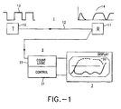
- high-speed communication system 1 consists of a transmitter 10 interconnected by a transmission facility 12 with a receiver 11. Information is transmitted to receiver 11 in a binary coded pulse format as a binary bit stream 13 applied to the input of transmission facility 12.
- Transmission facility 12 may be any one of a large number of high-speed transmission facilities such as coaxial cables, optical fibers, radio and satellite links or the like.
- the binary pulses of input binary bit stream 13 may be reconfigured by the characteristics of the transmission facility 12 and appear as the rounded binary coded pulse format shown as the binary bit stream 14 received by receiver 11.
- the binary pulse coded waveform measuring apparatus 2 as set forth in Fig.
- control 21 controls the operation of count logic 20 to generate a statistical eye diagram 30 representing the quality of the measured the binary pulse coded bit stream 14 on display apparatus 3 which may be any one of a number of well known display such as a computer or stand alone monitors, plotters, various storage devices, or the like.
- a pulse coded bit stream consists of a series of succeeding "0" and “1” pulses wherein each "0" pulse is transmitted at one voltage level and each "1" pulse is transmitted at another voltage level.
- the specific sequence of the of the "0" and “1” pulses define the information or data transmitted by transmitter 10 to receiver 11.
- the pulses have a repetition rate wherein each pulse has a period of time, hereinafter referred to as the pulse period, and follows a preceding pulse at the repetition rate determined by the communication system clock.
- Measuring apparatus or count logic 20, controlled by control 21, samples the pulse voltage levels in excess of voltage threshold levels during each of delayed clock pulses for a series of pulses of the binary coded pulse bit stream.
- Count logic 20 collects counts of the voltage of each pulse during the pulse period at variable voltage thresholds VVT occurring at voltage steps (V between a minimum voltage VMIN and a maximum voltage VMAX at a variable time delayed clock pulse TVD occurring in time steps (T between a range of zero and a selected maximum time TMAX.
- Control 21 coupled to the count logic 20 generates a series of the threshold voltage levels VVT and the delayed clock pulses TVD during each period of a bit stream pulse and accumulates multiple counts of the sampled pulse voltage levels in excess of the threshold voltage levels VVT during each delayed clock pulse TVD for a series of pulses of the binary coded pulse bit stream.
- the counts are recorded by control 21 as an Eye Data Array A1 2111 in memory 211 wherein the count data is stored at positions TVD, VVT in the array defined by the voltage threshold levels VVT separated by the voltage step (V and at ones of the delayed clock pulses TVD separated by the time step (T during pulse periods of the series of pulses succeeding the first measured binary pulse.
- the count starts in each pulse at time zero of the pulse period wherein counts of the pulse voltage level are taken and recorded in the Eye Data Array as the variable voltage threshold VVT is moved from the minimum voltage VMIN to the maximum voltage VMAX.
- the time delay clock pulse TVD is advanced in time a time step (T and the counting process repeated.
- the count measurement continues in (T steps until time TMAX is reached.
- the measurement of the counts may be continued over a large number of the bit stream pulses, for example, over several thousand serial pulses, with the total count being recorded in the eye data array.
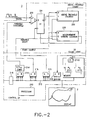
- the binary pulse coded waveform measuring apparatus 2, Fig. 2 comprises count logic 20 controlled by a control 21.
- Control processor 21 may be any one of a number of different types of computers and need not be described in great detail.
- control 21 has a processor 210 connected by a bus 212 to a memory 211 and a display unit 3.
- Processor 210 is also connected by bus 212 to address registers 213 and 215, the operation of the registers are well known. In the general operation, processor addresses address register 213 and requests that the count data received from the above threshold counter 202 of count logic 21 and stored in address register 213 be recorded in the eye data array A1, 2111 of memory 211.
- Processor 210 also addresses address registers 215 and transfers information thereto that is stored in the address registers and used to control various components in the count logic 20.
- the high-speed binary bit stream is applied to interface 216 so that processor 210 can generate clock pulses that are synchronous the repetition rate of the bit stream.
- Programs stored in memory 21 control processor 210 in the operation of the count logic 20 and control logic 21 in accordance with the principles of the invention.
- Count logic 20 has a one-bit comparator 200 with one input connected to the transmission facility 12 or other point in the transmitter 10 or receiver 11 to measure the high speed binary coded bit stream.
- the logic elements 200 and 201 are the main sampling components and are comprised of a D-type flip-flop 201 proceeded by a one-bit comparator 200.
- the one-bit comparator 200 will output a high when the signal voltage on the positive pin is higher than the signal voltage on the negative pin.
- the D-flip flop 201 will copy the value on the "D" input to the "Q" output connected to the enable input of the above threshold counter 202.
- processor 210 determining a pulse repetition rate of the high speed binary pulse bit stream by interface 216 and generates a series of the time delay clock pulses TVD each separated by a predefined time step (T during a period of each binary pulse and applies the time delay clock pulses TVD to the above threshold counter 202 and measurement window counter 203 via and address register 215.
- the above threshold counter 202 is a synchronous enableable and resetable counter and is of a type well known in the art. The counter will increment when not reset only when the enable line is "1" (high) at the rising edge of a clocking signal applied to the counter.
- threshold counter 202 holds the number of counts that succeeded in being higher then the voltage threshold VVT as the voltage threshold VVT is moved from the minimum voltage VMIN to the maximum voltage VMAX. threshold at the time of the rising edge of the time delay clock pulse TVD.
- the measurement window counter 203 is also a synchronous enableable and resetable counter and sets the measurement window size which sets the number of bits that are looked at to compute the "Above Threshold" count for each time delay clock pulse TVD and voltage threshold VVT position in the eye diagram.
- variable voltage threshold VVT is a static control voltage applied to the negative pin of comparator 200 and is set by processor 210 by addressing address register 215 to control the digital to VVT converter 214 to step this voltage in precise increments and apply the appropriate voltage step (V increment to the negative pin of comparator 200.
- Control 21 initiates the start sample sequence by applying a start pulse to reset the above threshold counter 202 and measurement counter 203 which start accumulating data. Once the measurement window counter 203 reaches it's terminal count, the apparatus will automatically stop and hold with the current "Above Threshold" count ready to be stored away. To start the next measurement, control 21 generates a new variable voltage threshold VVT and/or variable time delay clock pulse TVD and another start pulse.
- the measurement algorithm is stored in memory 211 and starts controlling control 1 to apply the start pulse to control logic 20.
- the initial value of the variable time delay pulse TVD is set to zero, step 21110, and values selected by the user are assigned to time TMAX, voltage VMAX, time step (T, voltage step (V and minimum voltage VMIN, step 21111. If the value of time delay pulse TVD is greater than the value of time TMAX, step 21112, the algorithm is completed. If not, the variable voltage threshold VVT is set to the value of minimum voltage VMIN, step 21113.
- Count logic 20 takes the count, step 21114, and records the count in eye diagram array (EDA) AI 2111 at the position EDA (time delay pulse TVD, variable voltage threshold VVT), step 21115.
- EDA eye diagram array
- variable voltage threshold VVT is increased by the value of the voltage step (V. If the new value of the variable voltage threshold VVT, step 21117, is less than the value of voltage VMAX, the algorithm repeats steps 21114 through 21116 to record counts in the eye data array 2111 at the appropriate time delay pulse TVD and variable voltage threshold VVT array positions.
- the time delay pulse TVD is increased by the time step (T, step 21118, steps 21112 through 21117 are repeated to record additional counts in the eye data array 2111 at the appropriate time delay pulse TVD and variable voltage threshold VVT array positions.
- the measurement algorithm is at an end, step 21119.
- the measurement may be repeated many times to determine the quality of a high speed binary pulse bit stream.
- the operation of the measurement algorithm has enabled processor 210, Fig. 2, to generate a first eye data array 2111 in memory 211 of the processor wherein the sampled pulse voltage level counts are recorded at array positions defined by ones of the variable voltage threshold levels VVT separated by the voltage step (V and at ones of the time delayed clock pulses TVD separated by the time step (T during the pulse periods.
- An example of an eye data array showing typical count data collected by the measuring algorithm of Fig. 3 is set forth in Fig.5 of the drawing wherein the count data is recorded at the array positions TVD, VVT wherein the time delay pulses TVD are separated by the time step (T and the variable voltage thresholds VVT are separated by the voltage step (V.
- the control 21 processor 210 operating under control of a processing algorithm program stored in memory 211 enables the processor210 to generate a second eye data array 2112 in memory 211.
- Processor 210 again under control of processing algorithm, processes the raw count data recorded in eye data array 2111 subtracting the pulse voltage count recorded in each time delay pulse TVD and voltage threshold VVT position plus one from the voltage threshold position VVT of each delayed clock pulse TVD and records the result as a count in a corresponding voltage threshold VVT and delayed clock position TVD of the second eye data array.
- the processor 210 displays the second eye data array 2112 as an eye diagram defining the characteristics and quality of the binary pulse bit stream.
- the processing algorithm starts by having the user set the values of time TMAX, voltage VMAX, the time step (T, the voltage step (V and the minimum voltage VMIN, step 21120.
- the value of the time delay pulse TVD is then set to zero, step 21121. If the value of the time delay pulse TVD is equal to or less than the value of time TMAX, step 21122, the value of variable voltage threshold VVT is set equal to value of the minimum voltage VMIN, step 2123.
- step 21124 When the value of the variable voltage threshold VVT is less than the value of the maximum voltage VMAX, step 21124, an eye data array 2 position TVD, VVT is set equal to the absolute value of the count recorded in the eye data array position time delay pulse TVD and variable voltage threshold VVT +1 subtracted from the count recorded in the eye data array position time delay pulse TVD and variable voltage threshold VVT.
- the variable voltage threshold VVT is increased by the value of the voltage step (V, step 21127 and the steps 21124 21124 through 1127 are repeated.
- step 21124 the value of the variable time delay pulse TVD is increased by (T and steps 21122 through 221124, 21126 and 21127 are repeated.
- the algorithm is completed when the value of the variable time delay pulse TVD is greater than the value of the maximum voltage TMAX.
- An example of the eye data array 2 2112 is set forth in Fig. 6 and has a count configuration off an eye diagram of the measured high speed binary pulse bit stream.
- Processor 210 is then enabled to display the processed count from eye data array2 2111 onto a display unit so that the eye diagram can be used to show the characteristics and quality of the measured binary pulse bit stream.
Landscapes
- Engineering & Computer Science (AREA)
- Quality & Reliability (AREA)
- Computer Networks & Wireless Communication (AREA)
- Signal Processing (AREA)
- Dc Digital Transmission (AREA)
Applications Claiming Priority (2)
| Application Number | Priority Date | Filing Date | Title |
|---|---|---|---|
| US09/541,970 US6728311B1 (en) | 2000-04-04 | 2000-04-04 | Apparatus and method for creating eye diagram |
| US541970 | 2000-04-04 |
Publications (2)
| Publication Number | Publication Date |
|---|---|
| EP1143654A2 true EP1143654A2 (fr) | 2001-10-10 |
| EP1143654A3 EP1143654A3 (fr) | 2003-11-26 |
Family
ID=24161814
Family Applications (1)
| Application Number | Title | Priority Date | Filing Date |
|---|---|---|---|
| EP01810333A Withdrawn EP1143654A3 (fr) | 2000-04-04 | 2001-04-03 | Système et procédé de mesure statistique de la figure en oeil d'un train de bits en série |
Country Status (3)
| Country | Link |
|---|---|
| US (1) | US6728311B1 (fr) |
| EP (1) | EP1143654A3 (fr) |
| JP (1) | JP2001352350A (fr) |
Cited By (16)
| Publication number | Priority date | Publication date | Assignee | Title |
|---|---|---|---|---|
| DE10241848A1 (de) * | 2002-09-09 | 2004-03-25 | Advico Microelectronics Gmbh | Verfahren zur Erfassung von optischen bzw. elektrischen Signalfolgen und Augenmonitor zur Erfassung und Darstellung von Signalfolgen |
| US6748338B2 (en) * | 2001-11-21 | 2004-06-08 | Winbond Electronics Corporation | Method and apparatus for testing eye diagram characteristics |
| US6768703B2 (en) * | 2002-04-25 | 2004-07-27 | Agilent Technologies, Inc. | Eye diagram analyzer with fixed data channel delays and swept clock channel delay |
| EP1460793A1 (fr) * | 2003-03-19 | 2004-09-22 | Synthesys Research, Inc. | Méthode et appareil pour compter les erreurs d'un signal qui sont en dehors des limites d'un masque en oeil |
| EP1460792A1 (fr) * | 2003-03-19 | 2004-09-22 | Synthesys Research, Inc. | Méthode et système pour la création d'un diagramme en oeil |
| US6810346B2 (en) * | 2002-01-31 | 2004-10-26 | Agilent Technologies, Inc. | Composite eye diagrams |
| GB2404445A (en) * | 2003-07-29 | 2005-02-02 | Agilent Technologies Inc | Eye diagram analyzer and method of measuring the level of a recurring data signal |
| WO2004105334A3 (fr) * | 2003-05-20 | 2005-06-02 | Rambus Inc | Procedes et circuits d'essai de marges |
| EP1306998A3 (fr) * | 2001-10-29 | 2005-07-13 | Agilent Technologies, Inc. | Procédé et dispositif de mesure de la figure en oeil |
| EP1560358A1 (fr) * | 2004-02-02 | 2005-08-03 | Synthesys Research, Inc. | Procédé et appareil pour la détermination de limites de performance d'après des mesures paramétriques |
| EP1640734A1 (fr) * | 2004-09-27 | 2006-03-29 | Synthesys Research, Inc. | Procédé et appareil pour mesurer la réponse en fréquence d'un récepteur numérique |
| US7336749B2 (en) | 2004-05-18 | 2008-02-26 | Rambus Inc. | Statistical margin test methods and circuits |
| US7363562B2 (en) * | 2004-09-27 | 2008-04-22 | Synthesys Research Inc | Method and apparatus for deferred decision signal quality analysis |
| US7408981B2 (en) | 2003-05-20 | 2008-08-05 | Rambus Inc. | Methods and circuits for performing margining tests in the presence of a decision feedback equalizer |
| US7590175B2 (en) | 2003-05-20 | 2009-09-15 | Rambus Inc. | DFE margin test methods and circuits that decouple sample and feedback timing |
| US7627029B2 (en) | 2003-05-20 | 2009-12-01 | Rambus Inc. | Margin test methods and circuits |
Families Citing this family (22)
| Publication number | Priority date | Publication date | Assignee | Title |
|---|---|---|---|---|
| US6629272B1 (en) * | 2000-11-09 | 2003-09-30 | Agilent Technologies, Inc. | Method and apparatus for displaying eye diagram on an error performance analyzer |
| US20030097226A1 (en) * | 2001-11-21 | 2003-05-22 | Synthesys | Apparatus and method for sampling eye diagrams with window comparators |
| US7606297B2 (en) * | 2002-03-15 | 2009-10-20 | Synthesys Research, Inc. | Method and system for creating an eye diagram using a binary data bit decision mechanism |
| US20040002847A1 (en) * | 2002-06-26 | 2004-01-01 | Sun Microsystems, Inc. | Method for creating and displaying signaling eye-plots |
| US7154944B2 (en) | 2002-10-31 | 2006-12-26 | Agilent Technologies, Inc. | Mask compliance testing using bit error ratio measurements |
| EP1376381A1 (fr) * | 2003-02-12 | 2004-01-02 | Agilent Technologies Inc | Méthode et système d'échantillonnage de données |
| JP4665116B2 (ja) * | 2003-04-14 | 2011-04-06 | エスティー‐エリクソン、ソシエテ、アノニム | ワイヤレス通信システムにおけるパルス検出 |
| US7467336B2 (en) * | 2004-02-02 | 2008-12-16 | Synthesys Research, Inc | Method and apparatus to measure and display data dependent eye diagrams |
| US7643576B2 (en) * | 2004-05-18 | 2010-01-05 | Avago Technologies General Ip (Singapore) Pte. Ltd. | Data-signal-recovery circuit, data-signal-characterizing circuit, and related integrated circuits, systems, and methods |
| US7539916B2 (en) | 2005-06-28 | 2009-05-26 | Intel Corporation | BIST to provide phase interpolator data and associated methods of operation |
| US7552366B2 (en) * | 2005-06-30 | 2009-06-23 | Intel Corporation | Jitter tolerance testing apparatus, systems, and methods |
| US7286947B1 (en) | 2006-04-13 | 2007-10-23 | International Business Machines Corporation | Method and apparatus for determining jitter and pulse width from clock signal comparisons |
| US7383160B1 (en) * | 2006-06-30 | 2008-06-03 | International Business Machines Corporation | Method and apparatus for constructing a synchronous signal diagram from asynchronously sampled data |
| US7389192B2 (en) * | 2006-06-30 | 2008-06-17 | International Business Machines Corporation | Determining data signal jitter via asynchronous sampling |
| US7684478B2 (en) * | 2006-06-30 | 2010-03-23 | International Business Machines Corporation | Generating an eye diagram of integrated circuit transmitted signals |
| US7783439B2 (en) * | 2006-10-13 | 2010-08-24 | International Business Machines Corporation | Signal generator device and data eye scan system |
| US7698669B1 (en) | 2007-05-11 | 2010-04-13 | Altera Corporation | Method and system to evaluate operational characteristics of an electronic circuit |
| JP5990947B2 (ja) * | 2012-03-13 | 2016-09-14 | 日産自動車株式会社 | 車両制御装置 |
| US8995514B1 (en) * | 2012-09-28 | 2015-03-31 | Xilinx, Inc. | Methods of and circuits for analyzing a phase of a clock signal for receiving data |
| US8885695B1 (en) | 2013-06-26 | 2014-11-11 | Global Unichip Corporation | Receiver circuit |
| US9071477B2 (en) | 2013-10-09 | 2015-06-30 | Global Unichip Corporation | Method and associated processing module for interconnection system |
| US9568548B1 (en) | 2015-10-14 | 2017-02-14 | International Business Machines Corporation | Measurement of signal delays in microprocessor integrated circuits with sub-picosecond accuracy using frequency stepping |
Family Cites Families (5)
| Publication number | Priority date | Publication date | Assignee | Title |
|---|---|---|---|---|
| US3721959A (en) * | 1971-11-29 | 1973-03-20 | Collins Radio Co | Method and means for detecting error rate of transmitted data |
| US4475210A (en) * | 1982-02-26 | 1984-10-02 | International Telephone And Telegraph Corporation | Data eye monitor |
| EP0448322A3 (en) * | 1990-03-23 | 1992-11-25 | Tektronix, Inc. | Automatic extraction of pulseparametrics from multi-valued functions |
| CA2056679C (fr) * | 1991-11-29 | 2002-02-12 | Timothy Joseph Nohara | Surveillance automatisee des conditions de canaux de communication numeriques utilisant les configurations de l'oeil |
| CA2249800C (fr) * | 1998-10-06 | 2003-12-09 | Northern Telecom Limited | Moniteur de qualite optique pour regenerateur 2r |
-
2000
- 2000-04-04 US US09/541,970 patent/US6728311B1/en not_active Expired - Lifetime
-
2001
- 2001-04-03 EP EP01810333A patent/EP1143654A3/fr not_active Withdrawn
- 2001-04-03 JP JP2001104354A patent/JP2001352350A/ja active Pending
Non-Patent Citations (1)
| Title |
|---|
| None * |
Cited By (31)
| Publication number | Priority date | Publication date | Assignee | Title |
|---|---|---|---|---|
| EP1306998A3 (fr) * | 2001-10-29 | 2005-07-13 | Agilent Technologies, Inc. | Procédé et dispositif de mesure de la figure en oeil |
| US6748338B2 (en) * | 2001-11-21 | 2004-06-08 | Winbond Electronics Corporation | Method and apparatus for testing eye diagram characteristics |
| US6810346B2 (en) * | 2002-01-31 | 2004-10-26 | Agilent Technologies, Inc. | Composite eye diagrams |
| US6768703B2 (en) * | 2002-04-25 | 2004-07-27 | Agilent Technologies, Inc. | Eye diagram analyzer with fixed data channel delays and swept clock channel delay |
| EP1359699A3 (fr) * | 2002-04-25 | 2005-07-13 | Agilent Technologies, Inc. | Dispositif de mesure de la figure en oeil |
| DE10241848B4 (de) * | 2002-09-09 | 2012-08-09 | Advico Microelectronics Gmbh | Verfahren zur Erfassung von optischen oder elektrischen Signalfolgen und Augenmonitor zur Durchführung des Verfahrens |
| DE10241848A1 (de) * | 2002-09-09 | 2004-03-25 | Advico Microelectronics Gmbh | Verfahren zur Erfassung von optischen bzw. elektrischen Signalfolgen und Augenmonitor zur Erfassung und Darstellung von Signalfolgen |
| US6961520B2 (en) | 2002-09-09 | 2005-11-01 | Advico Microelectronics Gmbh | Method for measurement of optical or electrical signal sequences and eye diagram monitor for measurement and display of signal sequences |
| EP1460792A1 (fr) * | 2003-03-19 | 2004-09-22 | Synthesys Research, Inc. | Méthode et système pour la création d'un diagramme en oeil |
| EP1460793A1 (fr) * | 2003-03-19 | 2004-09-22 | Synthesys Research, Inc. | Méthode et appareil pour compter les erreurs d'un signal qui sont en dehors des limites d'un masque en oeil |
| US10193642B2 (en) | 2003-05-20 | 2019-01-29 | Rambus Inc. | Margin test methods and circuits |
| US10735116B2 (en) | 2003-05-20 | 2020-08-04 | Rambus Inc. | Margin test methods and circuits |
| WO2004105334A3 (fr) * | 2003-05-20 | 2005-06-02 | Rambus Inc | Procedes et circuits d'essai de marges |
| US10880022B1 (en) | 2003-05-20 | 2020-12-29 | Rambus Inc. | Margin test methods and circuits |
| US11233589B2 (en) | 2003-05-20 | 2022-01-25 | Rambus Inc. | Margin test methods and circuits |
| US9544071B2 (en) | 2003-05-20 | 2017-01-10 | Rambus Inc. | Margin test methods and circuits |
| US9116810B2 (en) | 2003-05-20 | 2015-08-25 | Rambus Inc. | Margin test methods and circuits |
| US7408981B2 (en) | 2003-05-20 | 2008-08-05 | Rambus Inc. | Methods and circuits for performing margining tests in the presence of a decision feedback equalizer |
| US7590175B2 (en) | 2003-05-20 | 2009-09-15 | Rambus Inc. | DFE margin test methods and circuits that decouple sample and feedback timing |
| US7596175B2 (en) | 2003-05-20 | 2009-09-29 | Rambus Inc. | Methods and circuits for performing margining tests in the presence of a decision feedback equalizer |
| US7627029B2 (en) | 2003-05-20 | 2009-12-01 | Rambus Inc. | Margin test methods and circuits |
| US8817932B2 (en) | 2003-05-20 | 2014-08-26 | Rambus Inc. | Margin test methods and circuits |
| US8385492B2 (en) | 2003-05-20 | 2013-02-26 | Rambus Inc. | Receiver circuit architectures |
| GB2404445B (en) * | 2003-07-29 | 2006-10-18 | Agilent Technologies Inc | Eye diagram analyzer and method of measuring the level of a recurring data signal |
| US6901339B2 (en) | 2003-07-29 | 2005-05-31 | Agilent Technologies, Inc. | Eye diagram analyzer correctly samples low dv/dt voltages |
| GB2404445A (en) * | 2003-07-29 | 2005-02-02 | Agilent Technologies Inc | Eye diagram analyzer and method of measuring the level of a recurring data signal |
| EP1560358A1 (fr) * | 2004-02-02 | 2005-08-03 | Synthesys Research, Inc. | Procédé et appareil pour la détermination de limites de performance d'après des mesures paramétriques |
| US7336749B2 (en) | 2004-05-18 | 2008-02-26 | Rambus Inc. | Statistical margin test methods and circuits |
| US8023558B2 (en) * | 2004-09-27 | 2011-09-20 | Tektronix, Inc. | Method and apparatus for measuring the input frequency response of a digital receiver |
| US7363562B2 (en) * | 2004-09-27 | 2008-04-22 | Synthesys Research Inc | Method and apparatus for deferred decision signal quality analysis |
| EP1640734A1 (fr) * | 2004-09-27 | 2006-03-29 | Synthesys Research, Inc. | Procédé et appareil pour mesurer la réponse en fréquence d'un récepteur numérique |
Also Published As
| Publication number | Publication date |
|---|---|
| US6728311B1 (en) | 2004-04-27 |
| EP1143654A3 (fr) | 2003-11-26 |
| JP2001352350A (ja) | 2001-12-21 |
Similar Documents
| Publication | Publication Date | Title |
|---|---|---|
| US6728311B1 (en) | Apparatus and method for creating eye diagram | |
| US20080270053A1 (en) | Apparatus and method for sampling eye diagrams with window comparators | |
| US8024142B1 (en) | Method and system for analyzing signal waveforms | |
| US8489345B2 (en) | Technique for determining performance characteristics of electronic devices and systems | |
| US6492929B1 (en) | Analogue to digital converter and method of analogue to digital conversion with non-uniform sampling | |
| JP2775721B2 (ja) | ディジタルデータリンクの評価方法及びデータタイミングジッタの評価回路 | |
| US7606297B2 (en) | Method and system for creating an eye diagram using a binary data bit decision mechanism | |
| US11343067B2 (en) | Sampling point identification for low frequency asynchronous data capture | |
| US12592848B2 (en) | Data transmission chip and electronic device | |
| US7478011B2 (en) | Method and system for measuring signal characteristics of data signals transmitted between integrated circuit chips | |
| US6715112B2 (en) | Method and apparatus for displaying triggered waveform on an error performance analyzer | |
| US6115416A (en) | Pulse code sequence analyzer | |
| EP1437855A1 (fr) | Procédé pour la détermination d'une figure en oeil d'un signal digital | |
| US7339985B2 (en) | Zero crossing method of symbol rate and timing estimation | |
| US6775809B1 (en) | Technique for determining performance characteristics of electronic systems | |
| US4090242A (en) | Method and means for evaluating phase encoded communication systems | |
| US8378707B2 (en) | Evaluation of an output signal of a device under test | |
| US7573957B2 (en) | Strobe technique for recovering a clock in a digital signal | |
| WO2007038339A2 (fr) | Technique stroboscopique pour recuperer une horloge dans un signal numerique | |
| Kychak et al. | Initial data processing algorithms of bit error rate testers | |
| KR20240138909A (ko) | 아이 마진 테스트 방법 및 이를 기반으로 테스트 동작을 수행하는 전자 장치 | |
| EP1460792A1 (fr) | Méthode et système pour la création d'un diagramme en oeil | |
| US7064686B2 (en) | Method of determining a data rate and apparatus therefor | |
| EP0217607A2 (fr) | Circuit de réglage de la valeur de seuil pour une interface à signal vidéo et appareil d'enregistrement équipé de celui-ci | |
| US20080025448A1 (en) | Jitter characterization |
Legal Events
| Date | Code | Title | Description |
|---|---|---|---|
| PUAI | Public reference made under article 153(3) epc to a published international application that has entered the european phase |
Free format text: ORIGINAL CODE: 0009012 |
|
| AK | Designated contracting states |
Kind code of ref document: A2 Designated state(s): AT BE CH CY DE DK ES FI FR GB GR IE IT LI LU MC NL PT SE TR |
|
| AX | Request for extension of the european patent |
Free format text: AL;LT;LV;MK;RO;SI |
|
| PUAL | Search report despatched |
Free format text: ORIGINAL CODE: 0009013 |
|
| AK | Designated contracting states |
Kind code of ref document: A3 Designated state(s): AT BE CH CY DE DK ES FI FR GB GR IE IT LI LU MC NL PT SE TR |
|
| AX | Request for extension of the european patent |
Extension state: AL LT LV MK RO SI |
|
| 17P | Request for examination filed |
Effective date: 20040517 |
|
| AKX | Designation fees paid |
Designated state(s): DE FR GB |
|
| 17Q | First examination report despatched |
Effective date: 20050801 |
|
| STAA | Information on the status of an ep patent application or granted ep patent |
Free format text: STATUS: THE APPLICATION IS DEEMED TO BE WITHDRAWN |
|
| 18D | Application deemed to be withdrawn |
Effective date: 20081031 |