EP1146342A2 - Module électronique hyperfréquences et procédé de test du module - Google Patents
Module électronique hyperfréquences et procédé de test du module Download PDFInfo
- Publication number
- EP1146342A2 EP1146342A2 EP01400765A EP01400765A EP1146342A2 EP 1146342 A2 EP1146342 A2 EP 1146342A2 EP 01400765 A EP01400765 A EP 01400765A EP 01400765 A EP01400765 A EP 01400765A EP 1146342 A2 EP1146342 A2 EP 1146342A2
- Authority
- EP
- European Patent Office
- Prior art keywords
- line
- test
- pair
- electrical
- substrate
- Prior art date
- Legal status (The legal status is an assumption and is not a legal conclusion. Google has not performed a legal analysis and makes no representation as to the accuracy of the status listed.)
- Withdrawn
Links
Images

Classifications
-
- H—ELECTRICITY
- H05—ELECTRIC TECHNIQUES NOT OTHERWISE PROVIDED FOR
- H05K—PRINTED CIRCUITS; CASINGS OR CONSTRUCTIONAL DETAILS OF ELECTRIC APPARATUS; MANUFACTURE OF ASSEMBLAGES OF ELECTRICAL COMPONENTS
- H05K1/00—Printed circuits
- H05K1/02—Details
- H05K1/0266—Marks, test patterns or identification means
- H05K1/0268—Marks, test patterns or identification means for electrical inspection or testing
-
- G—PHYSICS
- G01—MEASURING; TESTING
- G01R—MEASURING ELECTRIC VARIABLES; MEASURING MAGNETIC VARIABLES
- G01R31/00—Arrangements for testing electric properties; Arrangements for locating electric faults; Arrangements for electrical testing characterised by what is being tested not provided for elsewhere
- G01R31/28—Testing of electronic circuits, e.g. by signal tracer
- G01R31/282—Testing of electronic circuits specially adapted for particular applications not provided for elsewhere
- G01R31/2822—Testing of electronic circuits specially adapted for particular applications not provided for elsewhere of microwave or radiofrequency circuits
-
- G—PHYSICS
- G01—MEASURING; TESTING
- G01R—MEASURING ELECTRIC VARIABLES; MEASURING MAGNETIC VARIABLES
- G01R31/00—Arrangements for testing electric properties; Arrangements for locating electric faults; Arrangements for electrical testing characterised by what is being tested not provided for elsewhere
- G01R31/28—Testing of electronic circuits, e.g. by signal tracer
- G01R31/2851—Testing of integrated circuits [IC]
- G01R31/2884—Testing of integrated circuits [IC] using dedicated test connectors, test elements or test circuits on the IC under test
-
- H—ELECTRICITY
- H05—ELECTRIC TECHNIQUES NOT OTHERWISE PROVIDED FOR
- H05K—PRINTED CIRCUITS; CASINGS OR CONSTRUCTIONAL DETAILS OF ELECTRIC APPARATUS; MANUFACTURE OF ASSEMBLAGES OF ELECTRICAL COMPONENTS
- H05K1/00—Printed circuits
- H05K1/02—Details
- H05K1/0213—Electrical arrangements not otherwise provided for
- H05K1/0237—High frequency adaptations
Definitions
- the invention relates to a microwave electronic module with built-in elements for testing the different functions of the module.
- the invention also relates to the method of test of such a module.
- An electronic microwave module is made up essentially of a substrate comprising electrical conductors printed on its faces and integrated circuits transferred to the substrate.
- the integrated circuits provide the various functions of the electronic module, knowledge, amplification, conversion, distribution etc., and have inputs and outputs usually having a characteristic impedance Z0.
- microwave electronic modules can integrate test elements to detect the failure of a or several functions of the module.
- the module includes additional test lines and outputs to isolate the component or the module function may be defective in order to perform its test.
- the Figures 1 and 2 show the block diagram of an electronic module 10 State of the art microwave using this technique.
- the module 10 has three functions, an input function 12 in series, via a distributor 14 and two connections 16 and 18, with two output functions 20 and 22 in parallel. These functions are interconnected by L electrical interconnection lines characteristic impedance microwave Z0.
- the module substrate has two derived lines Ld1, Ld2, of the same impedance characteristic Z0, provided for in the module design to carry out the tests.
- the module has an input E and a main output S and two test outputs S1 and S2 respectively connected to the derived lines Ld1 and Ld2.
- connection 16 and 18 (see figure 1) connecting this function to the functions of outlet are unsoldered from the substrate.
- the first derived line Ld1 is connected by one of its inputs at the output of the input function 12 to be tested using a test connection 24 soldered on the substrate (see Figure 2).
- a signal is then applied to the main input E.
- the signal at the output of the input function 12 is taken by a probe at the test output S1 of the derived line Ld1.
- connection 24 At the end of the test we desolder the connection 24 and we solder the connections 16 and 18 in order to return to the initial configuration of the module.
- This test technique requires an increase in the dimension of the module by implementing additional test lines often incompatible with product requirements. In addition, this technique is restrictive in the choice of functions to be tested and cannot be applied to all module functions.
- test tips are positioned using a machine directly at the inputs and outputs of the integrated circuit.
- This technique allows modules to be produced without integrated test elements the substrate.
- this technique has drawbacks important. On the one hand, given the size and geometry of the points of test, some functions too cashed in or too close to the walls of a module housing make the test impossible. On the other hand, the fact of cabling then rewiring the inputs and outputs of the integrated circuit can cause the degradation see the destruction of the component and especially when it comes to integrated circuits operating in millimeter waves.
- testing a component or function of the microwave electronic module is carried out by direct debit electromagnetic energy radiated by electrical connections between the elements to be tested.
- This technique is based on the coupling effect electromagnetic between a transmission line of the substrate and a probe test carried out for this purpose. This technique is not perfectly mastered and the test probe does not offer good accuracy in terms of measurement microwave signal can be picked up being of very low level and strongly disturbed.
- the invention is based on a microwave test technique original consisting in using microwave interconnection lines, which connect the different components or functions of the module, for the transform into conventional input / output impedance cells characteristic Z0.
- a microwave test technique original consisting in using microwave interconnection lines, which connect the different components or functions of the module, for the transform into conventional input / output impedance cells characteristic Z0.
- provision is made during the design phase of the module test metallizations printed on the substrate. These metallizations allow, with additional wiring when test, to get the input / output cells.
- This technique uses the property propagation of a microwave wave along a line of electrical transmission and in particular the fact that the line impedance at a quarter wave distance from a short circuit made on the line, is a strong impedance corresponding to an open circuit.
- test tip microwave of characteristic impedance Z0, positioned on the line at this quarter-wave distance of the short circuit, will behave like a load suitable for the circuit to be tested. In addition, the probe will not disturbed by a signal on the line from the short circuit side.
- the length electrical line must be at least a quarter wave or ⁇ t / 4.
- electrical interconnection lines between circuits integrated (or module functions) are interconnection lines of micro-band type with characteristic impedance Z0.
- a first electrical conductor of the line in the form of a metallic ribbon, is printed on one side of the substrate, a second ground conductor is printed on the other side of the substrate parallel to the first, this second ground conductor covering the first conductor on the line.
- this configuration almost all of the electric field lines between the two conductors of the line cross the thickness of the substrate.
- the substrate has at least two pairs of pads metallic, each metallic pad of a pair being opposite one of the other and on both sides of the electrical conductor of the line interconnection, the metal pads being of dimensions, in the plane of the substrate, much smaller than the length of the interconnect line.
- test can be performed on complex modules with several lines and many interconnected components, the module being originally designed with test elements, as defined in the invention, arranged on certain lines so as to perform the test of predetermined functions.
- the component can itself be a complex function consisting of sets of integrated circuits and passive circuits adapted in impedance and connected to the adapted microwave interconnection lines of same impedance.
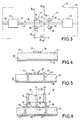
- Figure 3 shows a partial view of an electronic module microwave 30 according to the invention, comprising test elements at a frequency Ft predetermined at module design.
- the module 30 comprises a substrate 32 on which are transferred a first integrated circuit 34 and a second integrated circuit 36.
- the electrical length of the line is at least equal to or greater than a quarter of the wavelength ⁇ t of the test frequency Ft so that the tests can be carried out according to the procedure of the invention.
- the interconnection line 38 microwave is of the micro-band type.
- Figure 4 shows a view in section AA 'of the substrate 32 at the interconnection line 38.
- the substrate 32 has two metallized faces, a front face 44 on which an electrical conductor 46 of line 38 is printed in the form of a ribbon metallic and a rear face 48 comprising a ground conductor 50 covering the conductor 46 over its entire length.
- the characteristic impedance Z0 of line 38 is determined from the thickness of the substrate 32, its dielectric constant and the width of the electrical conductor of the line.
- the substrate 32 comprises two pairs P1, P2 of two areas each, respectively 52, 54 and 56, 58, the metal pads of each of the pairs being located on either side of the conductor 46 of line 36 and facing each other, the metal areas being dimensions, in the plane of the substrate, much smaller than the length of the interconnection line between the two integrated circuits.
- the first pair P1 is located on the side of the first function 34 and the second pair P2 on the side of the second function 36 and at an electrical distance from the first pair P1 substantially equal to the quarter wave ⁇ t / 4 of the test frequency Ft.
- FIG. 5 shows a sectional view BB 'of the substrate 32 at the level of the first pair P1 of the metal pads 52, 54.
- the pads are connected to the ground conductor 50 of the face 48 of the substrate by metallized holes 59.
- Figure 6 shows a simplified sectional view of such a probe 60 placed on a test point of a microwave line 62, of the micro-band type, a microwave module to be tested.
- Line 62 carried out on a substrate 64 has an electrical conductor 66 on one face of the substrate and a ground conductor 68 on the other face.
- the coaxial probe 60 comprises an insulator 70 having a core 72 coaxial (hot spot) and a shield 74.
- a tip 76 of the core 72 of the probe and two metal tabs 78 surrounding the free part of the core 72 are respectively brought into contact with the electrical conductor 66 of line 62 and metallic areas 80 of mass located on the same face.
- the transfer of the ground conductor 68 from the line to the face of the substrate comprising the electrical conductor 66 of the line carried out by holes metallic 67.
- the probe is charged by the characteristic impedance Z0.
- This guy suitable probe ensures in a test procedure according to the invention, a good adaptation of the function to be tested.
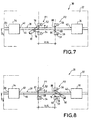
- test of the two functions 34 and 36 of the module is carried out from the as follows:
- a test signal appearing at output 40 of this first function 34 is propagated on line 38.
- the short circuit on line 38, at the level of the second pair P2 is translated, at the test frequency Ft, by a high impedance of the line at level of the first pair P1.
- the output 40 of the first circuit 34 is charged, across line 38, to the characteristic impedance Z0 of the probe, which makes it possible to carry out the test of the first integrated circuit 32 on a adapted load of impedance Z0.
- the short circuit of line 38 at the level of the second pair P2 reduces any disturbance on the test probe 60 applied to the line 38 by a signal from input 42 of the second circuit integrated 36.
- a test signal appearing at input 42 of the second function 36 propagates on line 38.
- the short circuit produced on line 38, at the level of the first pair P1 is translated, at the test frequency Ft, by a high impedance of the line at the level of the second pair P2.
- the entrance 42 of the second circuit 36 is loaded, across line 38, on the characteristic impedance Z0 of the probe 60, which makes it possible to carry out the test of the second integrated circuit 36 on a suitable load of impedance Z0.
- the short circuit of line 38 on the side of the first circuit 34 avoids any disturbance on the test probe 60 by a signal from the output 40 of this first integrated circuit 34.
- the metal areas of the two pairs P1 and P2 include protrusions 88 (see FIGS. 3, 6 and 7) of very small width compared to dimensions of the metal areas.
- the distance between the pairs P1, P2 of metal areas is linked at the frequency used for the test and conditions the band of use of a such a device, theoretically applicable to a single frequency.
- the test principle according to the invention can, in practice, be used over a width bandwidth of 10% around the frequency for which the quarter distance waveform has been calculated.
- a test In a degraded mode, a test, with a slightly adapted load cell (line and probe) of the function to be tested, can be performed in a larger bandwidth of the order of 20% around the calculated frequency.
- the implementation of the test method according to the invention makes it possible to diagnose a fault at a frequency particular of the product specification strip, which turns out, in the majority of cases, sufficient to determine the module or function in breakdown.
- test procedure according to the invention lies in the fact that for some microwave modules already studied, it is possible to easily add the two pairs of metal pads to use this procedure.
- the substrate of the electronic module includes a third pair P3 of metal pads which makes it possible to carry out the test according to the invention on another frequency Ft '.
- the second pair P2 is located at a first quarter wave ⁇ t / 4 from the first pair P1, the third pair P3 being located at a second quarter wave ⁇ t '/ 4 of this first pair P1, which makes it possible to carry out the test respectively at the first test frequency Ft and at a second test frequency Ft '.
- the test procedure is the same that in the case of the module comprising two pairs but a first time, at frequency Ft using the first and second pair and a second time at frequency Ft 'using the first and third pair.
- two metal areas of at least one of the two pairs are lengthened parallel to the electrical conductor of the line.
- This configuration on pain of a slight disturbance in the line adaptation due to the presence near the electrical conductor of the line, longer length metallized areas, allows for a test over a range of test frequencies.
- This frequency range corresponding to a range of possible electrical distances between a first pair of very short length Lg and both ends of the second pair of longer metal pads.
- the probe can be placed at a point on the line located at any point on the line between the ends of the metal pads of the second pair. If the probe is placed at the first pair, the short circuit can be made at any point on the line located between the ends of the metal pads of the second pair.
- the module electronics according to the invention operates at 10 GHz
- the substrate has a thickness of 0.38 millimeters and the electrical conductor of the line interconnection 38 a width of 380 micrometers.
- the distance d separating the metal ranges of the line is of the order of 450 micrometers.
- the quarter the wavelength is 2.9 millimeters.
- test cell To use the test cell as access for both circuits microwave to be tested directly on the module, it must be defined from the design phase the operating mode allowing access to the cells test with microwave probes. Most often the tips standard with an angle of inclination from the plane of the substrate of 45 degrees allow this access, in some cases vertical points can be used.
- test cell line and probe
- mismatch of the test circuit is low, the reflection coefficient being greater than 20 dB and the variation in losses less than -0.05 dB.
Landscapes
- Engineering & Computer Science (AREA)
- Microelectronics & Electronic Packaging (AREA)
- General Engineering & Computer Science (AREA)
- Physics & Mathematics (AREA)
- General Physics & Mathematics (AREA)
- Computer Hardware Design (AREA)
- Testing Of Individual Semiconductor Devices (AREA)
- Tests Of Electronic Circuits (AREA)
Abstract
Description
- un substrat métallisé ayant deux faces principales, des conducteurs électriques imprimés sur ces faces et parmi ces conducteurs des conducteurs de masse reliés à une masse du module électronique ;
- des composants reportés sur le substrat ;
- au moins une ligne d'interconnexion électrique entre deux composants, la ligne d'interconnexion d'impédance caractéristique Z0 étant formée par un conducteur électrique et au moins un conducteur de masse, caractérisé en ce que le substrat comporte sur la face ayant le conducteur électrique de la ligne d'interconnexion, de part et d'autre de ce conducteur électrique, des plages métalliques reliées aux conducteurs de masse, ces plages métalliques étant destinées à effecteur un test électrique hyperfréquence, à au moins une fréquence de test Ft, des composants reliés par la ligne.
- un substrat métallisé ayant deux faces principales, des conducteurs électriques imprimés sur les faces et parmi ces conducteurs des conducteurs de masse reliés à une masse du module électronique ;
- des composants reportés sur le substrat ;
- au moins une ligne d'interconnexion électrique entre deux composants, la ligne d'interconnexion, d'impédance caractéristique Z0, étant formée par un conducteur électrique et au moins un conducteur de masse, le substrat comportant sur la face ayant le conducteur électrique de la ligne d'interconnexion, de part et d'autre de ce conducteur électrique, des plages métalliques reliées aux conducteurs de masse, caractérisé en ce qu'il comporte au moins les étapes suivantes :
- réalisation d'un court circuit en un premier point de la ligne entre un premier point du conducteur électrique de la ligne et les plages métalliques de masse ;
- application d'une sonde de test d'impédance caractéristique Z0 sur un second point de la ligne entre un second point du conducteur électrique et les plages de masse, ce second point étant distant du court-circuit (premier point) d'une longueur électrique sensiblement égale au quart d'onde λt/4 de la fréquence de test Ft ;
- application d'un signal hyperfréquence de test, à la fréquence de test Ft, à un accès d'un des composants à tester ;
- prélèvement par la sonde de test du signal de sortie apparaissant sur ce second point de la ligne.
- les figures 1 et 2 représentent le synoptique d'un module électronique hyperfréquences de l'état de l'art ;
- la figure 3 montre une vue partielle d'un module électronique hyperfréquence selon l'invention ;
- les figures 4 et 5 montrent des vues en coupe du substrat du module de la figure 3 ;
- la figure 6 montre une vue simplifiée en coupe d'une sonde de test hyperfréquences ;
- la figure 7 représente une vue partielle du module de la figure 3 lors d'une première phase de la procédure de test.
- la figure 8 représente la vue partielle du module de la figure 3 lors d'une deuxième phase de la procédure de test.
- mise en court-circuit à la masse de la ligne 38 (voir figure 7) au niveau de deuxième paire P2 en reliant, par soudure d'une connexion métallique 84, le conducteur électrique 46 et les plages métalliques 56, 58 de la seconde paire P2.
- application de la sonde de test 60 hyperfréquence sur la ligne 38 au niveau de la première paire P1 en appliquant la pointe 76 de la sonde 60 (point chaud) et ses languettes de masse 78 respectivement sur le conducteur électrique 46 et les plages métalliques 52, 54 de la première paire P1.
- injection d'un signal de test St à la fréquence de test Ft, à une entrée 86 de la première fonction 34, à l'aide d'une sonde d'injection (non représentée) semblable à la sonde 60.
- mise en court-circuit à la masse de la ligne 38 (voir figure8) au niveau de la première paire P1 en reliant, par soudure d'une connexion métallique 87, le conducteur électrique 46 et les plages métalliques 52, 54 de cette première paire P1.
- application de la sonde de test 60 hyperfréquence sur la ligne 38 au niveau de la deuxième paire P2 en appliquant la pointe 76 de la sonde (point chaud) et ses languettes de masse 78 respectivement sur le conducteur électrique 46 et les plages métalliques 56, 58 de la deuxième paire P2.
- injection d'un signal de test St à l'entrée 86 de la première fonction 34 à l'aide d'une sonde d'injection (non représentée) semblable à la sonde de test 60.
Claims (9)
- Module électronique hyperfréquences comportant :un substrat (32) métallisé ayant deux faces principales (44, 48), des conducteurs électriques (46, 50, 66, 68) imprimés sur ces faces et parmi ces conducteurs des conducteurs de masse (50, 68) reliés à une masse du module électronique ;des composants (12, 20, 22, 34, 36) reportés sur le substrat ;au moins une ligne (L, 38) d'interconnexion électrique entre deux composants, la ligne d'interconnexion, d'impédance caractéristique Z0 étant formée par un conducteur électrique (46, 66) et au moins un conducteur de masse (50, 68), caractérisé en ce que le substrat (32) comporte sur la face (44) ayant le conducteur électrique (46) de la ligne (38) d'interconnexion, de part et d'autre de ce conducteur électrique, des plages métalliques (52, 54, 56, 58) reliées aux conducteurs de masse (50), ces plages métalliques étant destinées à effecteur un test électrique hyperfréquence, à au moins une fréquence de test Ft, des composants reliés par la ligne.
- Module électronique selon la revendication 1, caractérisé en ce que la ligne d'interconnexion électrique (38) entre les deux circuits intégrés (34, 36) est une ligne micro-bande d'impédance caractéristique Z0, un premier conducteur électrique (46) de la ligne se trouvant sur une des faces (44) du substrat, le second conducteur de masse (50) se trouvant sur l'autre face (48) du substrat, parallèle au premier conducteur.
- Module électronique selon la revendication 2, caractérisé en ce que le substrat comporte au moins deux paires P1, P2 de plages métalliques (52, 54, 56, 58), chaque plage métallique d'une paire étant en vis-à-vis l'une de l'autre et de part et d'autre du conducteur électrique (46) de la ligne (38) d'interconnexion, les plages métalliques étant de dimensions, dans le plan du substrat, bien plus petites que la longueur de la ligne d'interconnexion.
- Module électronique selon la revendication 3, caractérisé en ce que les plages métalliques comportent des excroissances (88) de très faible largeur par rapport aux dimensions des plages métalliques, ces excroissances dirigées vers le conducteur électrique (46) de la ligne (38) rapprochant la masse métallique du conducteur électrique de la ligne.
- Module électronique selon l'une des revendications 1 à 4, caractérisé en ce que le substrat comporte une troisième paire P3 de plages métalliques, la deuxième paire P2 étant située à un premier quart d'onde λt/4 de la première paire P1, la troisième paire P3 étant située à un second quart d'onde λt'/4 de cette première paire P1, permettant d'effectuer respectivement le test à la première fréquence de test Ft et à une deuxième fréquence de test Ft'.
- Module électronique selon l'une des revendications 3 à 5, caractérisé en ce que deux plages métalliques d'au moins une des deux paires sont allongées parallèlement au conducteur électrique de la ligne, permettant d'effecteur un test sur une plage de fréquences de test.
- Procédé de test électrique d'un module électronique hyperfréquences, le test étant effectué à au moins une fréquence de test Ft, le module électronique comportant :un substrat (32) métallisé ayant deux faces principales (44, 48), des conducteurs électriques (46, 50, 66, 68) imprimés sur les faces et parmi ces conducteurs des conducteurs de masse (58, 68) reliés à une masse du module électronique ;des composants (12, 20, 22, 34, 36) reportés sur le substrat ;au moins une ligne (L, 38) d'interconnexion électrique entre deux composants, la ligne d'interconnexion, d'impédance caractéristique Z0, étant formée par un conducteur électrique (46, 66) et au moins un conducteur de masse (50, 68), le substrat (32) comportant sur la face (44) ayant le conducteur électrique (46) de la ligne (38) d'interconnexion, de part et d'autre de ce conducteur électrique, des plages métalliques (52, 54, 56, 58) reliées aux conducteurs de masse (50), caractérisé en ce qu'il comporte au moins les étapes suivantes:réalisation d'un court circuit en un premier point de la ligne entre un premier point du conducteur électrique de la ligne et les plages métalliques de masse ;application d'une sonde de test (60) d'impédance caractéristique Z0 sur un second point de la ligne entre un second point du conducteur électrique et les plages de masse, ce second point étant distant du court-circuit d'une longueur électrique sensiblement égale au quart d'onde λt/4 de la fréquence de test Ft ;application d'un signal hyperfréquence de test, à la fréquence de test Ft, à un accès (86) d'un des composants à tester ;prélèvement par la sonde de test du signal de sortie apparaissant sur ce second point de la ligne (38).
- Procédé de test électrique selon la revendication 7, le module comportant ùn premier (34) et un deuxième (36) circuits intégrés reliés par une ligne (38) d'interconnexion électrique, le substrat du module comportant deux paires P1, P2 de plages métalliques (52, 54, 56, 58), chaque plage métallique d'une paire étant en vis-à-vis l'une de l'autre et de part et d'autre du conducteur électrique (46) de la ligne (38) d'interconnexion, les plages métalliques étant de dimensions, dans le plan du substrat, bien plus petites que la longueur de la ligne d'interconnexion entre les deux circuits intégrés, la première paire P1 étant située du côté du premier circuit intégré 34 et la deuxième paire P2 du côté du deuxième circuit intégré (36) et à une distance électrique de la première paire P1 sensiblement égale au quart d'onde λt/4 de la fréquence de test Ft, caractérisé en ce que dans une première phase on effectue le test du premier circuit intégré (34), par la réalisation d'au moins les opérations suivantes :mise en court-circuit à la masse de la ligne (38) au niveau de deuxième paire P2 en reliant par une connexion métallique (84) le conducteur électrique (46) et les plages métalliques (56, 58) de la seconde paire P2.application de la sonde de test (60) hyperfréquence sur la ligne (38) au niveau de la première paire P1 ;injection d'un signal de test St à la fréquence de test Ft, à une entrée (86) du premier circuit intégré (34), à l'aide d'une sonde ;retrait de la sonde de test (60) et de la connexion métallique (84) ramenant la ligne (38) et le module dans leur état initial ; et en ce que dans une seconde phase on effectue le test du deuxième circuit intégré (36) par la réalisation des opérations suivantes:mise en court-circuit à la masse de la ligne (38) au niveau de la première paire P1 en reliant par une connexion métallique (87) le conducteur électrique (46) et les plages métalliques (52, 54) de cette première paire P1.application de la sonde de test (60) hyperfréquence sur la ligne (38) au niveau de la deuxième paire P2.injection d'un signal de test St à l'entrée (86) du premier circuit intégré (34) à l'aide d'une sonde d'injection.retrait de la sonde de test (60) et de la connexion électrique (86) ramenant la ligne (38) et le module dans leur état initial.
- Procédé de test électrique selon la revendication 8, le substrat du module électronique comportant en outre une troisième paire P3 de plages métalliques, la deuxième paire P2 étant située au premier quart d'onde λt/4 de la première paire P1, la troisième paire P3 étant située à un second quart d'onde λt'/4 de cette première paire P1, caractérisé en ce que l'on effectué une première fois la procédure de test à la fréquence Ft en utilisant la première et la deuxième paire et une seconde fois à une autre fréquence Ft' en utilisant la première P1 et la troisième paire P3.
Applications Claiming Priority (2)
| Application Number | Priority Date | Filing Date | Title |
|---|---|---|---|
| FR0004133 | 2000-03-31 | ||
| FR0004133A FR2807207B1 (fr) | 2000-03-31 | 2000-03-31 | Module electronique hyperfrequences et procede de test du module |
Publications (2)
| Publication Number | Publication Date |
|---|---|
| EP1146342A2 true EP1146342A2 (fr) | 2001-10-17 |
| EP1146342A3 EP1146342A3 (fr) | 2003-12-17 |
Family
ID=8848728
Family Applications (1)
| Application Number | Title | Priority Date | Filing Date |
|---|---|---|---|
| EP01400765A Withdrawn EP1146342A3 (fr) | 2000-03-31 | 2001-03-23 | Module électronique hyperfréquences et procédé de test du module |
Country Status (2)
| Country | Link |
|---|---|
| EP (1) | EP1146342A3 (fr) |
| FR (1) | FR2807207B1 (fr) |
Family Cites Families (4)
| Publication number | Priority date | Publication date | Assignee | Title |
|---|---|---|---|---|
| FR2532120A3 (fr) * | 1982-08-17 | 1984-02-24 | Thomson Brandt | Coupleur hyperfrequence selectif |
| JPH0260204A (ja) * | 1988-08-25 | 1990-02-28 | Matsushita Electric Ind Co Ltd | マイクロ波集積回路 |
| FR2678436B1 (fr) * | 1991-06-28 | 1993-10-15 | Telecommunicat Radioelect Teleph | Prise coaxiale pour circuit hyperfrequence. |
| DE4315276A1 (de) * | 1993-05-07 | 1994-11-10 | Siemens Ag | Schaltungsanordnung zur richtungsabhängigen Auskopplung von Mikrowellensignalen aus einer Leitung |
-
2000
- 2000-03-31 FR FR0004133A patent/FR2807207B1/fr not_active Expired - Fee Related
-
2001
- 2001-03-23 EP EP01400765A patent/EP1146342A3/fr not_active Withdrawn
Also Published As
| Publication number | Publication date |
|---|---|
| FR2807207A1 (fr) | 2001-10-05 |
| EP1146342A3 (fr) | 2003-12-17 |
| FR2807207B1 (fr) | 2002-06-21 |
Similar Documents
| Publication | Publication Date | Title |
|---|---|---|
| FR2797351A1 (fr) | Dispositif d'alimentation de ligne en forme de bande | |
| FR2911190A1 (fr) | Testeur pour transmission de signaux a haute frequence et carte sonde utilisant celui-ci. | |
| FR2648236A1 (fr) | Appareil de mesure d'impedance surfacique | |
| FR2621130A1 (fr) | Dispositif de mesure de produits d'intermodulation d'un systeme recepteur | |
| EP0454578B1 (fr) | Procédé pour vérifier l'efficacité du blindage électromagnétique d'un cordon conducteur, et dispositif pour la mise en oeuvre du procédé | |
| EP1146342A2 (fr) | Module électronique hyperfréquences et procédé de test du module | |
| EP0534826B1 (fr) | Dispositif pour tests hyperfréquences à large bande réalisés in situ | |
| FR2666452A1 (fr) | Module de circuit a semiconducteurs multicouche. | |
| EP1342094B1 (fr) | Dispositif de caracterisation electromagnetique d'une structure sous test | |
| WO2001055739A1 (fr) | Procede et dispositif de controle d'un cable de telecommunication | |
| FR3110293A1 (fr) | Antenne active incluant un cadre blindé | |
| WO2008141902A1 (fr) | Coupleur de signaux hyperfrequences en technologie microruban | |
| EP0596773A1 (fr) | Dispositif pour tests hyperfréquences à large bande réalisés in situ | |
| EP3301751B1 (fr) | Dispositif électronique à antenne isolée | |
| EP0983616B1 (fr) | Procede et dispositif pour connecter deux elements millimetriques | |
| FR3107788A1 (fr) | Antenne active comportant un cadre blindé | |
| EP0514250B1 (fr) | Dispositif pour tests hyperfréquences à large bande réalisés in situ | |
| FR2696009A1 (fr) | Dispositif de calibrage pour ajuster en hyperfréquence les plans de référence d'un appareillage de mesure des paramètres de dispersion d'éléments de circuits intégrés. | |
| EP1210611B1 (fr) | Procede de mesure et de diagnostic de rayonnements electromagnetiques | |
| FR2644896A1 (fr) | Carte a pointes pour le test des composants semi-conducteurs hyperfrequences | |
| FR2616973A1 (fr) | Ligne de transmission hyperfrequence a deux conducteurs coplanaires | |
| WO2009127695A1 (fr) | Procede de test de câbles avec insertion de dispositif de couplage directionnel | |
| FR2670296A1 (fr) | Dispositif de mesure de l'impedance de transfert d'un cable. | |
| EP1227331A2 (fr) | Circuit d'excitation et de récupération du signal émis par une sonde dans un appareil de spectrométrie RMN | |
| WO1990008327A2 (fr) | Systeme d'interface de mesure par un analyseur logique des signaux numeriques d'un circuit integre |
Legal Events
| Date | Code | Title | Description |
|---|---|---|---|
| PUAI | Public reference made under article 153(3) epc to a published international application that has entered the european phase |
Free format text: ORIGINAL CODE: 0009012 |
|
| AK | Designated contracting states |
Kind code of ref document: A2 Designated state(s): AT BE CH CY DE DK ES FI FR GB GR IE IT LI LU MC NL PT SE TR |
|
| AX | Request for extension of the european patent |
Free format text: AL;LT;LV;MK;RO;SI |
|
| PUAL | Search report despatched |
Free format text: ORIGINAL CODE: 0009013 |
|
| AK | Designated contracting states |
Kind code of ref document: A3 Designated state(s): AT BE CH CY DE DK ES FI FR GB GR IE IT LI LU MC NL PT SE TR |
|
| AX | Request for extension of the european patent |
Extension state: AL LT LV MK RO SI |
|
| AKX | Designation fees paid | ||
| REG | Reference to a national code |
Ref country code: DE Ref legal event code: 8566 |
|
| STAA | Information on the status of an ep patent application or granted ep patent |
Free format text: STATUS: THE APPLICATION IS DEEMED TO BE WITHDRAWN |
|
| 18D | Application deemed to be withdrawn |
Effective date: 20040618 |