EP1146550A2 - Verfahren zur Herstellung von Verbindungsleitungen in einem integrierten Schaltkreis - Google Patents
Verfahren zur Herstellung von Verbindungsleitungen in einem integrierten Schaltkreis Download PDFInfo
- Publication number
- EP1146550A2 EP1146550A2 EP01400287A EP01400287A EP1146550A2 EP 1146550 A2 EP1146550 A2 EP 1146550A2 EP 01400287 A EP01400287 A EP 01400287A EP 01400287 A EP01400287 A EP 01400287A EP 1146550 A2 EP1146550 A2 EP 1146550A2
- Authority
- EP
- European Patent Office
- Prior art keywords
- cavity
- titanium
- track
- copper
- layer
- Prior art date
- Legal status (The legal status is an assumption and is not a legal conclusion. Google has not performed a legal analysis and makes no representation as to the accuracy of the status listed.)
- Withdrawn
Links
Images

Classifications
-
- H—ELECTRICITY
- H10—SEMICONDUCTOR DEVICES; ELECTRIC SOLID-STATE DEVICES NOT OTHERWISE PROVIDED FOR
- H10W—GENERIC PACKAGES, INTERCONNECTIONS, CONNECTORS OR OTHER CONSTRUCTIONAL DETAILS OF DEVICES COVERED BY CLASS H10
- H10W20/00—Interconnections in chips, wafers or substrates
- H10W20/40—Interconnections external to wafers or substrates, e.g. back-end-of-line [BEOL] metallisations or vias connecting to gate electrodes
- H10W20/41—Interconnections external to wafers or substrates, e.g. back-end-of-line [BEOL] metallisations or vias connecting to gate electrodes characterised by their conductive parts
- H10W20/425—Barrier, adhesion or liner layers
-
- H—ELECTRICITY
- H10—SEMICONDUCTOR DEVICES; ELECTRIC SOLID-STATE DEVICES NOT OTHERWISE PROVIDED FOR
- H10W—GENERIC PACKAGES, INTERCONNECTIONS, CONNECTORS OR OTHER CONSTRUCTIONAL DETAILS OF DEVICES COVERED BY CLASS H10
- H10W20/00—Interconnections in chips, wafers or substrates
- H10W20/40—Interconnections external to wafers or substrates, e.g. back-end-of-line [BEOL] metallisations or vias connecting to gate electrodes
- H10W20/41—Interconnections external to wafers or substrates, e.g. back-end-of-line [BEOL] metallisations or vias connecting to gate electrodes characterised by their conductive parts
- H10W20/42—Vias, e.g. via plugs
Definitions
- the invention relates to the manufacture of integrated circuits, and more particularly the production of metal tracks using a process of the "damascene" type, according to a name well known to man of the job.
- a damascene process can be carried out according to several variants.
- the track is made in providing a cavity in the inter-track dielectric disposed at metallization considered, then filling the cavity with a metal of filling, for example copper, after depositing in the bottom and on the sides of the cavity a conductive barrier layer, for example in tantalum nitride.
- the manufacturing of the integrated circuit also includes the deposit an encapsulation layer, typically made of silicon nitride, on the metallization level.
- This deposition is carried out conventionally at high temperature, typically at 400 ° C.
- manufacturing an integrated circuit requires other heat treatments, for example after each oxide deposition.
- small amounts of silicon can diffuse into the copper tracks from the nitride encapsulation layer of silicon. This then results in a significant increase in the resistivity of metal tracks.
- the invention aims to provide a solution to this problem and proposes a radically different solution to avoid increasing the resistance of metal tracks due to diffusion of silicon in the copper.
- the invention therefore provides a method of manufacturing a circuit integrated, including a production phase, at a metallization level predetermined, of at least one metallic track within a material dielectric interpiste, this phase of realization comprising an engraving dielectric material interoperates so as to form a cavity at the place from said track, the deposition in the cavity of a conductive barrier layer, for example in tantalum nitride, filling the cavity with copper and the deposition on the predetermined metallization level of a layer of silicon nitride.
- the phase of realization of the metal track further comprises, between the deposition step of the barrier layer and the copper filling step, a deposit of titanium on at least part of the barrier layer.
- the silicon in the silicon nitride layer diffuses in the copper tracks, under significant thermal budgets, for example greater than or equal to 400 ° C., the silicon forms with the titanium a titanium silicide TiSi 2 .
- the silicon that diffuses in copper is thus trapped by titanium, which preserves the low resistivity of copper.
- the layer of titanium hugs the walls of the cavity perfectly perfectly continuous, since its sole purpose is to extract copper from the diffused silicon (by transformation into titanium silicide). So, he it is possible to deposit this titanium with a simple spray, for example using an argon plasma which strikes a target in titanium.
- the deposition of titanium by spraying is sufficient to deposit titanium particles at the top of the cavity, this which has the advantage of being as close as possible to the layer of silicon nitride.
- non-reactive ion etching is carried out titanium deposited in the cavity, with a plasma flow perpendicular to the bottom of the cavity. This removes the titanium from the bottom of the cavity and thus avoiding the risk of an increase in the resistance of the line (track). And, this non-reactive ion etching with a plasma flow perpendicular to the bottom of the cavity, allows the titanium particles on the vertical sides of the cavity, and in particular those close to the upper edge of the cavity.
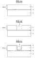
- the reference 1 designates a layer of an inter-track dielectric material, for example SiO 2 formed from ethyl tetraorthosilicate (Si (OC 2 H 5 ) 4 ; TEOS in English)). It is inside this layer 1 that the metal tracks of metallization level n will be produced.
- SiO 2 formed from ethyl tetraorthosilicate (Si (OC 2 H 5 ) 4 ; TEOS in English)
- This dielectric layer 1 rests on an encapsulation layer 2, having a thickness of the order of 120 nm, and typically made of silicon nitride SiN or more generally of Si x N y .
- This encapsulation layer 2 is deposited on a layer of an inter-level dielectric material, for example also SiO 2 formed from ethyl tetraorthosilicate, and which separates the metal level n from the lower metal level n- 1.
- This inter-level dielectric layer typically has a thickness of 800 nm.
- the next step ( Figure 1b) consists, using methods conventional photolithography, to engrave the material inter-track dielectric 1, with stop on the encapsulation layer 2, of so as to provide cavities 4 (only one of these cavities is shown on Figure 1b) at the location of future metal tracks.
- the encapsulation layer 2 serves, on the one hand to avoid contamination of the inter-level dielectric by the copper of the level n track, on the other hand of stop layer for etching of the cavity.
- a barrier layer is deposited (FIG. 1c) conductive 5, typically made of tantalum nitride or else titanium nitride.
- This layer with a thickness of a few tens of nanometers, for example 25 nm, serves as a barrier to the diffusion of copper particles in the inter-track dielectric.
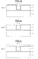
- a titanium deposition is then carried out (FIG. 1d) by spraying, for example using an argon-based plasma which comes hit a titanium target at room temperature under a pressure of 1 Torr.
- the titanium particles 6 are then sprayed on the sides and the bottom of the cavity 4 as well as on the surface of the barrier layer 5.
- This cleaning step removes the titanium from the bottom of the cavity, which will avoid a risk of increasing the resistance of the track subsequent metal.
- the invention therefore has the advantage of not affecting the low resistivity of copper on metal tracks while avoiding causing damage to the integrated circuit transistors.
- the invention is not limited to the so-called variant "simple damascene" which has just been described. It also applies in particular to the variant called “self-aligned double damascene” in which simultaneously etches the cavities of the connections vertical metal (commonly known to those skilled in the art “vias”) and cavities of the future tracks of the metallization level superior.
Landscapes
- Internal Circuitry In Semiconductor Integrated Circuit Devices (AREA)
Applications Claiming Priority (2)
| Application Number | Priority Date | Filing Date | Title |
|---|---|---|---|
| FR0001801 | 2000-02-14 | ||
| FR0001801A FR2805084B1 (fr) | 2000-02-14 | 2000-02-14 | Procede de fabrication de pistes metalliques pour des circuits integres |
Publications (2)
| Publication Number | Publication Date |
|---|---|
| EP1146550A2 true EP1146550A2 (de) | 2001-10-17 |
| EP1146550A3 EP1146550A3 (de) | 2002-01-16 |
Family
ID=8846973
Family Applications (1)
| Application Number | Title | Priority Date | Filing Date |
|---|---|---|---|
| EP01400287A Withdrawn EP1146550A3 (de) | 2000-02-14 | 2001-02-06 | Verfahren zur Herstellung von Verbindungsleitungen in einem integrierten Schaltkreis |
Country Status (4)
| Country | Link |
|---|---|
| US (1) | US6528419B1 (de) |
| EP (1) | EP1146550A3 (de) |
| JP (1) | JP2001230257A (de) |
| FR (1) | FR2805084B1 (de) |
Families Citing this family (6)
| Publication number | Priority date | Publication date | Assignee | Title |
|---|---|---|---|---|
| JP4447438B2 (ja) * | 2004-11-29 | 2010-04-07 | Necエレクトロニクス株式会社 | 半導体装置の製造方法 |
| WO2008028851A1 (en) * | 2006-09-04 | 2008-03-13 | Koninklijke Philips Electronics N.V. | Control of carbon nanostructure growth in an interconnect structure |
| WO2008065125A1 (en) * | 2006-11-29 | 2008-06-05 | Nxp B.V. | Fabrication of a diffusion barrier cap on copper containing conductive elements |
| US7964934B1 (en) | 2007-05-22 | 2011-06-21 | National Semiconductor Corporation | Fuse target and method of forming the fuse target in a copper process flow |
| US8030733B1 (en) | 2007-05-22 | 2011-10-04 | National Semiconductor Corporation | Copper-compatible fuse target |
| US7709956B2 (en) * | 2008-09-15 | 2010-05-04 | National Semiconductor Corporation | Copper-topped interconnect structure that has thin and thick copper traces and method of forming the copper-topped interconnect structure |
Family Cites Families (12)
| Publication number | Priority date | Publication date | Assignee | Title |
|---|---|---|---|---|
| KR960001601B1 (ko) * | 1992-01-23 | 1996-02-02 | 삼성전자주식회사 | 반도체 장치의 접촉구 매몰방법 및 구조 |
| JP2728025B2 (ja) * | 1995-04-13 | 1998-03-18 | 日本電気株式会社 | 半導体装置の製造方法 |
| JPH1187349A (ja) * | 1997-07-16 | 1999-03-30 | Mitsubishi Electric Corp | 半導体装置の製造方法及び半導体装置 |
| US5821168A (en) * | 1997-07-16 | 1998-10-13 | Motorola, Inc. | Process for forming a semiconductor device |
| JPH11145138A (ja) * | 1997-11-10 | 1999-05-28 | Hitachi Ltd | 半導体装置およびその製造方法 |
| JP3500564B2 (ja) * | 1997-12-19 | 2004-02-23 | 富士通株式会社 | 半導体装置の製造方法 |
| US6218302B1 (en) * | 1998-07-21 | 2001-04-17 | Motorola Inc. | Method for forming a semiconductor device |
| US6093632A (en) * | 1998-12-07 | 2000-07-25 | Industrial Technology Research Institute | Modified dual damascene process |
| US6225210B1 (en) * | 1998-12-09 | 2001-05-01 | Advanced Micro Devices, Inc. | High density capping layers with improved adhesion to copper interconnects |
| US6258707B1 (en) * | 1999-01-07 | 2001-07-10 | International Business Machines Corporation | Triple damascence tungsten-copper interconnect structure |
| US6100181A (en) * | 1999-05-05 | 2000-08-08 | Advanced Micro Devices, Inc. | Low dielectric constant coating of conductive material in a damascene process for semiconductors |
| US6197681B1 (en) * | 1999-12-31 | 2001-03-06 | United Microelectronics Corp. | Forming copper interconnects in dielectric materials with low constant dielectrics |
-
2000
- 2000-02-14 FR FR0001801A patent/FR2805084B1/fr not_active Expired - Fee Related
-
2001
- 2001-02-06 EP EP01400287A patent/EP1146550A3/de not_active Withdrawn
- 2001-02-07 JP JP2001031574A patent/JP2001230257A/ja active Pending
- 2001-02-21 US US09/790,259 patent/US6528419B1/en not_active Expired - Fee Related
Also Published As
| Publication number | Publication date |
|---|---|
| US6528419B1 (en) | 2003-03-04 |
| EP1146550A3 (de) | 2002-01-16 |
| FR2805084B1 (fr) | 2003-09-26 |
| FR2805084A1 (fr) | 2001-08-17 |
| JP2001230257A (ja) | 2001-08-24 |
Similar Documents
| Publication | Publication Date | Title |
|---|---|---|
| EP0351001B1 (de) | Verfahren zur Herstellung einer Halbleitervorrichtung mit mindestens einer kleine Kontaktlöcher enthaltenden Leiterbahn | |
| US5147819A (en) | Semiconductor metallization method | |
| EP0325808B1 (de) | Verfahren, um eine elektrische Verbindung auf einer Silizium-Halbleitervorrichtung herzustellen | |
| US6334249B2 (en) | Cavity-filling method for reducing surface topography and roughness | |
| JP3006735B2 (ja) | 半導体装置およびその製造方法 | |
| FR2630588A1 (fr) | Procede pour realiser une configuration d'interconnexion sur un dispositif semiconducteur notamment un circuit a densite d'integration elevee | |
| FR2757312A1 (fr) | Transistor mis a grille metallique auto-alignee et son procede de fabrication | |
| JPH06216263A (ja) | 半導体装置の配線層形成方法 | |
| US5985751A (en) | Process for fabricating interconnection of semiconductor device | |
| JP2001085438A (ja) | 集積回路デバイスの製造中に銅配線を形成する方法 | |
| FR2764734A1 (fr) | Procede de formation de plots de contact d'un dispositif a semiconducteur | |
| FR2805084A1 (fr) | Procede de fabrication de pistes metalliques pour des circuits integres | |
| FR3000840A1 (fr) | Procede de realisation de contacts metalliques au sein d'un circuit integre, et circuit integre correspondant | |
| FR2853134A1 (fr) | Procede de fabrication d'un transistor a grille metallique, et transistor correspondant | |
| FR2763424A1 (fr) | Processus de damasquinage double | |
| CN101034682B (zh) | 半导体装置及其制造方法 | |
| FR3082050A1 (fr) | Via interne avec contact ameliore pour couche semi-conductrice superieure d'un circuit 3d | |
| WO2004057658A2 (fr) | Transistor mis a grille auto-alignee et son procede de fabrication | |
| FR2782841A1 (fr) | Procede permettant de former des plots de contact et, en meme temps, de rendre plane une surface de substrat dans des circuits integres | |
| EP0933812B1 (de) | Elektrochemische Abscheidung von Metallen in Halbleiteranordnungen | |
| FR2947384A1 (fr) | Procede de realisation d'un transistor a source et drain metalliques | |
| FR2713397A1 (fr) | Procédé de formation de couches métalliques minces et épaisses. | |
| EP1650796A2 (de) | Verfahren für einen Kontaktanschluss auf einer Region einer integrierten Schaltung, insbesondere auf Transistorelektroden | |
| EP3072148B1 (de) | Verfahren zum schutz einer silizidschicht | |
| JPH11354466A (ja) | 接点用開口を有する半導体基板に接点を形成する方法 |
Legal Events
| Date | Code | Title | Description |
|---|---|---|---|
| PUAI | Public reference made under article 153(3) epc to a published international application that has entered the european phase |
Free format text: ORIGINAL CODE: 0009012 |
|
| AK | Designated contracting states |
Kind code of ref document: A2 Designated state(s): AT BE CH CY DE DK ES FI FR GB GR IE IT LI LU MC NL PT SE TR Kind code of ref document: A2 Designated state(s): DE FR GB IT |
|
| AX | Request for extension of the european patent |
Free format text: AL;LT;LV;MK;RO;SI |
|
| PUAL | Search report despatched |
Free format text: ORIGINAL CODE: 0009013 |
|
| RAP1 | Party data changed (applicant data changed or rights of an application transferred) |
Owner name: KONINKLIJKE PHILIPS ELECTRONICS N.V. Owner name: STMICROELECTRONICS S.A. |
|
| AK | Designated contracting states |
Kind code of ref document: A3 Designated state(s): AT BE CH CY DE DK ES FI FR GB GR IE IT LI LU MC NL PT SE TR |
|
| AX | Request for extension of the european patent |
Free format text: AL;LT;LV;MK;RO;SI |
|
| 17P | Request for examination filed |
Effective date: 20020708 |
|
| AKX | Designation fees paid |
Free format text: DE FR GB IT |
|
| 17Q | First examination report despatched |
Effective date: 20071009 |
|
| RAP1 | Party data changed (applicant data changed or rights of an application transferred) |
Owner name: NXP B.V. Owner name: STMICROELECTRONICS S.A. |
|
| STAA | Information on the status of an ep patent application or granted ep patent |
Free format text: STATUS: THE APPLICATION IS DEEMED TO BE WITHDRAWN |
|
| 18D | Application deemed to be withdrawn |
Effective date: 20141209 |