EP1146565A2 - Dispositif d'affichage à vue directe - Google Patents
Dispositif d'affichage à vue directe Download PDFInfo
- Publication number
- EP1146565A2 EP1146565A2 EP01303285A EP01303285A EP1146565A2 EP 1146565 A2 EP1146565 A2 EP 1146565A2 EP 01303285 A EP01303285 A EP 01303285A EP 01303285 A EP01303285 A EP 01303285A EP 1146565 A2 EP1146565 A2 EP 1146565A2
- Authority
- EP
- European Patent Office
- Prior art keywords
- organic
- film
- display
- substrate
- circuit
- Prior art date
- Legal status (The legal status is an assumption and is not a legal conclusion. Google has not performed a legal analysis and makes no representation as to the accuracy of the status listed.)
- Granted
Links
Images



Classifications
-
- H—ELECTRICITY
- H10—SEMICONDUCTOR DEVICES; ELECTRIC SOLID-STATE DEVICES NOT OTHERWISE PROVIDED FOR
- H10K—ORGANIC ELECTRIC SOLID-STATE DEVICES
- H10K59/00—Integrated devices, or assemblies of multiple devices, comprising at least one organic light-emitting element covered by group H10K50/00
- H10K59/10—OLED displays
- H10K59/18—Tiled displays
-
- H—ELECTRICITY
- H10—SEMICONDUCTOR DEVICES; ELECTRIC SOLID-STATE DEVICES NOT OTHERWISE PROVIDED FOR
- H10K—ORGANIC ELECTRIC SOLID-STATE DEVICES
- H10K59/00—Integrated devices, or assemblies of multiple devices, comprising at least one organic light-emitting element covered by group H10K50/00
- H10K59/10—OLED displays
- H10K59/17—Passive-matrix OLED displays
- H10K59/179—Interconnections, e.g. wiring lines or terminals
Definitions
- the present invention relates to a direct-view-type display apparatus using organic thin-film EL elements as display elements, for example, and particularly to a direct-view-type display apparatus suitable for realizing a large display screen.
- EL (electroluminescent) elements are known as a kind of light-emitting display elements. EL elements make use of an electro-luminescence as a principle which is a phenomenon in which a light is produced from a phosphor when applied with a voltage.
- EL elements are classified into an inorganic EL element in which rare earth element serving as a center of light emission is added to a host material made of an inorganic compound and an organic EL element using a fluorescent organic compound. From a standpoint of a physical shape of a light-emitting material, EL elements are classified as a dispersion-type EL element using a powder-like light-emitting material and a thin-film EL element using a dense thin-film-like light-emitting material.
- the organic thin-film EL element is able to display colors that matches with fluorescent colors of organic compounds so that colors can be selected with ease as compared with the inorganic EL element, it can be driven by a low drive voltage as compared with the inorganic EL element and it can easily be manufactured by microminiaturization as compared with the inorganic EL element, in recent years, it is receiving a remarkable attention as a display element for use in a direct-view-type display apparatus.
- the direct-view-type display apparatus using this organic thin-film EL element (hereinafter simply referred to as an "organic EL display”) has an advantage that it can be well confirmed visually as compared with display apparatus using a non-light-emitting display element such as a liquid crystal and has also an advantage that it can do with a low driving voltage as compared with display apparatus using a display element of another light-emitting type (e.g., plasma display and field-emission display) so that it consumes less power and it can be expected that ICs for driving this type of display element can be manufacured inexpensively.
- a non-light-emitting display element such as a liquid crystal
- a display element of another light-emitting type e.g., plasma display and field-emission display
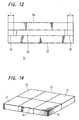
- FIG. 13 shows an example of an arrangement of this display unit.
- a display unit 51 is manufactured such that a protecting film (not shown) made of an inorganic compound such as GeO is formed on the surface of an organic thin-film EL element 53 formed on a glass substrate 52 or a light-curing resin layer (not shown) is formed directly or through an SiO2 film on which a glass plate 54 having the same area as that of the glass substrate 52 is tightly contacted and the glass plate 54 and the glass substrate 52 are bonded together at end portions of their plate surfaces by an adhesive agent 55 having an end-sealing property.
- FIG. 14 shows an example in which a plurality of display units 51 shown in FIG. 13 are disposed in a matrix fashion.
- the reason that the organic thin-film EL element is sealed by the glass plate 54 and the adhesive agent 55 as shown in FIG. 13 is as follows. That is, an organic compound used in an organic layer of the organic thin-film EL element is considerably weak to water and oxygen, and metals comprising anodes and cathodes of the organic thin-film EL element also are oxidized in the air and their characteristics are deteriorated suddenly.
- the present invention is intended to realize the organic EL display with the large picture screen and to do away with the above disadvantage (a) and to simplify the fabrication work and to reduce the manufacturing cost, to do away with the above disadvantage (b) and to maintain the periodicity with which the pixels are arrayed on the whole of the picture screen after fabrication, to do away with the above disadvantage (c) and to prevent a picture quality from being deteriorated due to the boundary between the transparent substrates, and to do away with the above disadvantage (d) and to realize the picture screen of the high resolution.
- a direct-view-type display apparatus is characterized in that a plurality of display elements are formed on a single transparent substrate and driver circuits for supplying signals to signal electrodes and scanning electrodes of these display elements are provided in response to respective display elements.
- a plurality of display elements are not formed as units like the prior art but are formed on a single, common transparent substrate. Then, when signals are supplied to the respective display elements from the corresponding driver circuits, an image is displayed on one picture screen of this transparent substrate.
- the periodicity with which the pixels are arrayed on the whole of the picture screen can be maintained without positioning the display units with high accuracy unlike the prior art, the large picture screen can be realized, the fabrication work can be simplified and the manufacturing cost can be reduced.
- the positional relationship between the display elements can be prevented from being shifted after fabrication unlike the case in which a plurality of display units are disposed in a matrix fashion, the periodicity with which the pixels are disposed on the whole of the picture screen can be maintained after fabrication.
- the picture quality can be prevented from being deteriorated due to the above boundary.
- the circuit substrate on which the driver circuits are mounted in response to the respective display elements are disposed on the back side (opposite to the display surface).
- the positioning of the circuit substrate relative to the display element is required to such an extent that the driver circuits may electrically be connected to the electrodes of the display elements, the highly-accurate positioning of the display units is not required unlike the prior art. Therefore, the fabrication work can be prevented from becoming complicated and the manufacturing cost can be prevented from being increased.
- the height of the signal electrode and the height of the scanning electrode of the organic EL element on the transparent substrate are made substantially equal to each other.
- the circuit substrate is made of a material having end-sealing property and has through-holes bored at its positions opposing to the signal electrode and the scanning electrode. The through-holes are buried by a material having end-sealing property and conductivity. While the through-holes are being opposed to the signal electrode and the scanning electrode, the circuit substrate is closely bonded to the organic EL element. signals are supplied from the driver circuit through the material having the end-sealing property and the conductivity.
- the organic EL element is covered at its portion which is not bonded to the circuit substrate with an end-sealing material.
- the organic EL element is sealed by the circuit substrate, the material having an end-sealing property and a conductivity and the end-sealing material while the space between the adjacent organic EL element on the transparent substrate is being kept narrow, the pixel pitch can be reduced, and therefore the organic EL display with high resolution can be realised.
- the transparent substrate should be formed of a film-like substrate. According to this arrangement, not only a flat picture screen can be formed but also a curved picture screen can be formed by curving this transparent substrate.
- the side surface of the circuit substrate should be covered with a member having an elasticity. According to this arrangement, even if the circuit boards are butted against each other when the circuit boards are disposed or the curved picture screen is formed by curving the transparent substrate, the circuit boards can be prevented from being chipped or scratched.
- the hereinafter described embodiments of the present invention can provide a direct-view-type display apparatus other than the organic EL display in which a large picture screen can be realised, the fabrication work can be simplified, the manufacturing cost can be reduced, the periodicity with which the pixels are arrayed on the whole of the picture screen can be maintained and the deterioration of the picture quality can be prevented.
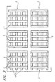
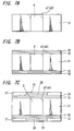
- FIG. 1 shows an example of an arrangement of an outward appearance of a panel portion of an organic EL display to which the present invention is applied from the panel display surface side.
- this organic EL display a plurality of organic thin-film elements 2 are formed in a matrix fashion on the rear surface (surface on the opposite side of the panel display surface) of one glass transparent substrate 1.
- the transparent substrate 1 has a dimension corresponding to a screen size of indoor and outdoor big-screen display.
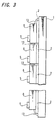
- FIGS. 2 and 3 show examples of arrangements of individual thin-film EL elements 2 of this organic EL display from the panel display surface side and the side surface side, respectively.
- each organic thin-film EL element 2 includes anodes (signal electrodes) 3 and cathodes (scanning electrodes) 4, each of which is a predetermined number (e.g., four).
- a space between the adjacent organic thin-film EL element 2 is made equal to a space between these electrodes within the organic thin-film EL element 2, whereby periodicity with which pixels are arrayed on the whole of the screen is maintained.
- the signal electrode 3 is formed of a transparent electrode made of ITO (indium-tin oxide), for example.
- the scanning electrode 4 is formed of an electrode made of metal alloy such as aluminum and lithium.
- the signal electrodes 3 As a method of forming the signal electrodes 3, there is used a method in which after a signal electrode had been formed over substantially the whole range of the longitudinal direction of the transparent substrate 1, for example, this signal electrode is removed by etching at portions corresponding to the boundaries of the respective organic thin-film EL element 2 in the longitudinal direction of the transparent substrate 1. Consequently, the signal electrodes 3 of each organic thin-film EL element 2 are formed at the same time.
- the scanning electrodes 4 As a method of forming the scanning electrodes 4, there is used a method in which after portions corresponding to boundaries of the respective organic thin-film EL elements 2 in the lateral direction of the transparent substrate 1, for example, has been masked, a metal which serves as a material of the scanning electrodes 4 is deposited over substantially the whole range of the lateral direction of the transparent substrate 1 by vapor deposition. Consequently, the scanning electrodes 4 of each organic thin-film EL element 2 also are formed at the same time.
- a circuit substrates 5 are disposed on the rear surface side (the opposite side of the panel display surface) in response to the respective organic thin-film EL elements 2.
- the circuit substrate 5 has mounted thereon a driver circuit 6 for supplying signals (display signal and scanning signal) to the signal electrode 3 and the scanning electrode 4 of the corresponding organic thin-film EL element 2.
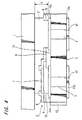
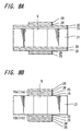
- FIG. 4 is a diagram showing more in detail the structure of the organic thin-film EL element 2 and the circuit substrate 5 from the side surface side.
- the signal electrode 3 of each organic thin-film EL element 2 has a range (height h in the sheet of drawing) in which its height on the transparent substrate 1 is substantially equal to the scanning electrode 4 (height h in the sheet of drawing) at a portion which is not intersected by the scanning electrode 4.
- a thin-film like organic layer 7 is formed at a portion (pixel portion) at which the signal electrode 3 and the scanning electrode 4 cross with each other.
- the organic layer 7 is comprised of an organic hole transport layer, an organic light-emitting layer and an organic electron transport layer (as another example, the organic layer is comprised of only the organic hole transport layer and an organic light-emitting layer having an electron transport property), though not shown.
- the signal electrode 3 and the scanning electrode 4 are separated by an insulating layer 8 formed on the signal electrode 3 by vapor deposition.
- the circuit substrate 5 is the substrate made of the same glass as that of the transparent substrate 1.
- the circuit substrate 5 has a through-hole a1 within the area opposing to the range (height h) in which the height of each signal electrode 3 of the organic thin-film EL element 2 is substantially equal to the scanning electrode 4 and has also a through-hole a2 within the area opposing to the range excepting the portion (pixel portion) in which each scanning electrode 4 of the organic thin-film EL element 2 and the signal electrode 3 cross each other.
- the respective through-holes a1, a2 are buried with conductive pastes (e.g., silver pastes) 9 using epoxy resin as a binder, respectively.
- the silver pastes 9 of the respective through-holes a1 are covered at respective substrate surfaces of the circuit substrate 5 with metal films 10a and 10b consisting of four layers of chromium, copper, nickel and gold.
- the silver pastes 9 of the respective through-holes 2a are covered at respective substrate surfaces of the circuit board 5 with metal films 11a and 11b having the same structures as those of the metal films 10a and 10b.
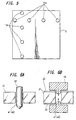
- FIG. 5 shows the positions of the metal films 10a, 11a on the circuit substrate 5 from the substrate surface side.
- the side surface of the circuit substrate 5 is covered with a protecting film 12 made of silicon rubber.
- the circuit substrate 5 is closely joined to the organic thin-film EL element 2 in the way that the respective metal films 10a, 11a are respectively contacted with the signal electrode 3 and the scanning electrode 4.
- thermoplastic resin 15 As a method of joining the circuit substrate 5 and the organic thin-film EL element 2, while polyester, vinyl chloride, vinyl acetate, polyamide or polyurethane thermoplastic resin 15 is being softened by heating, after this thermoplastic resin has been coated on the circuit substrate 5 at its portions other than the metal films 10a and 11a and the circuit substrate 5 and the organic thin-film EL element 2 have been put into pressurized contact with each other, this thermoplastic resin 15 is cooled and cured.
- each organic thin-film EL element 2 is covered at its portion, which is not joined to the circuit substrate 5, with an end-sealing material 13 made of epoxy resin which is resin having end-sealing property.
- an adhesive agent made of epoxy resin for example, has been coated, such adhesive agent is cured.
- the driver circuit 6 on each circuit substrate 5 supplies a signal to the signal electrode 3 of the corresponding organic thin-film EL element 2 through the wiring formed on the substrate surface of the circuit substrate 5 and the metal film 10b, the silver paste 9 and the metal film 10a shown in FIG. 4, and also supplies a signal to the scanning electrode 4 of the corresponding organic thin-film EL element 2 through the interconnection formed on the substrate surface of the circuit substrate 5 and the metal film 11b, the silver paste 9 and the metal film 11a shown in FIG. 4, whereby an image is displayed on the transparent substrate 1 which is served as one screen.
- the organic thin-film EL elements 2 can be prevented from being shifted from each other in the positional relationship after the manufacturing, and hence the periodicity with which the pixels are arrayed on the whole of the screen can be maintained after the manufacturing.
- the boundary between the transparent substrates of the display units does not exist, it is possible to prevent the picture quality from being deteriorated due to this boundary.
- the organic thin-film EL element 2 While the space between the adjacent organic thin-film EL elements 2 on the transparent substrate 1 is being kept narrow (while this space is being kept equal to the space between the signal electrode 3 and the scanning electrode 4 within the organic thin-film EL element 2), the organic thin-film EL element 2 is sealed by the circuit substrate 5 made of glass, the metal films 10a, 10b, 11a, 11b and the end-sealing material 13. Accordingly, since the pixel pitch can be reduced, the organic EL display with high resolution can be realized.
- the circuit substrate 5 has only to be positioned with respect to the organic thin-film EL element 2 in a way that the through-holes a1, a2 are brought in contact with the signal electrode 3 and the scanning electrode 4, respectively (i.e., in a way that the driver circuit 6 is electrically connected to the signal electrode 3 and the scanning electrode 4).
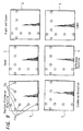
- FIG. 9 shows the state in which the positions of the five circuit substrates 5 of the circuit substrates 5 corresponding to the adjacent six organic thin-film EL elements 2 on the transparent substrate 1 are roughly shifted from the reference position (the position at which the circuit substrate is accurately disposed with respect to the organic thin-film EL element 2) to some extent such as in the counter-clockwise direction, in the upper direction, in the right and lower direction, in the clockwise direction and in the lower directio when they are seen from the panel display surface side.
- the reference position the position at which the circuit substrate is accurately disposed with respect to the organic thin-film EL element 2
- some extent such as in the counter-clockwise direction, in the upper direction, in the right and lower direction, in the clockwise direction and in the lower directio when they are seen from the panel display surface side.
- FIG. 10 shows a positional relationship among the signal electrode 3, the scanning electrode 4 and the metal films 10a, 11a obtained when the circuit substrates 5 are bonded to the organic thin-film EL elements 2 in the state shown in FIG. 9.
- the respective organic thin-film EL elements 2 to which the circuit substrates 5, which are positionally shifted, are bonded as for part of the signal electrode 3 and the scanning electrode 4 (the signal electrode 3 and the scanning electrode 4 which are most largely shifted from the metal films 10a, 11a in the organic thin-film EL element 2 to which the circuit substrates 5 shifted in the counter-clockwise direction and in the clockwise direction are bonded), ranges (the range of the height h in FIG. 4) in which the metal films 10a, 11a are contacted are shown hatched.
- the circuit substrate 5 Since the side surface of the circuit substrate 5 is covered with the protecting film 12 made of silicon rubber, even if the circuit substrates 5 butt into each other when the circuit substrates 5 are disposed on the elements, the circuit substrates 5 can be prevented from being cracked and scratched.
- the present invention is not limited thereto and there may be used a transparent substrate made of a resin (acrylic resin such as PMMA (polymethyl methacrylate)).
- acrylic resin such as PMMA (polymethyl methacrylate)
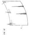
- a thin film-like transparent substrate 14 as shown in FIG. 11, whereby not only a flat screen can be formed but also a curved-surface-like screen can be formed by curving this film-like transparent substrate 14 slightly in the lateral direction as shown in FIG. 12 (while a convex surface-like screen is formed as shown in the sheet of drawing, it is needless to say that a concave surface-like screen can be formed). Further, since the side surface of the circuit substrate 5 is covered with the protecting film 12, even if the circuit substrates 5 butt into each other when the film-like transparent substrate 14 is curved, the circuit substrates 5 can be prevented from being cracked and scratched.
- each organic thin-film EL element 2 includes four signal electrodes 3 and four scanning electrodes 4 in the above example, the number of the signal electrodes 3 and the scanning electrodes 4 of each organic thin-film EL element 2 may be no more than than three or no less than five.
- the range in which the height on the transparent substrate 1 is substantially equal to the scanning electrode 4 is provided at the portion in which the signal electrode 3 of the organic thin-film EL element 2 does not cross the scanning electrode 4.
- a gold bump instead of providing the range in which the height on the transparent substrate 1 is high in the signal electrode 3, a gold bump may be formed on the silver paste within the through-hole of the circuit substrate 5 and this gold bump and the signal electrode 3 may be contacted with each other.
- the big-screen organic EL display is comprised of the single transparent substrate 1 in the above example
- the present invention is not limited thereto and a bigger-screen organic EL display may be formed by disposing a plurality of transparent substrates 1 in a matrix fashion.
- the number of the transparent substrates 1 thus disposed is considerably less than the number of display units required when one organic thin-film EL element is formed as units like the prior art, the fabrication work can be prevented from becoming complicated and the manufacturing cost can be prevented from being increased.
- the present invention is applied to the panel driven by a simple XY-matrix type in which the organic layer 7 is provided between the signal electrode 3 and the scanning electrode 4 as described above, the present invention is not limited thereto and can be applied to an active matrix type panel in which a TFT (thin film transistor) is formed on each organic EL element 2 and each organic EL element 2 is actively driven based on signals from the signal electrode 3 and the scanning electrode 4.
- a TFT thin film transistor
- the big-screen can be realized, the fabrication work can be simplified, the manufacturing cost can be reduced, the periodicity with which the pixels are arrayed on the whole of the screen can be maintained after the manufacturing, and the picture quality can be prevented from being deteriorated.
Landscapes
- Electroluminescent Light Sources (AREA)
- Devices For Indicating Variable Information By Combining Individual Elements (AREA)
- Control Of Indicators Other Than Cathode Ray Tubes (AREA)
- Control Of El Displays (AREA)
Applications Claiming Priority (2)
| Application Number | Priority Date | Filing Date | Title |
|---|---|---|---|
| JP2000109665 | 2000-04-11 | ||
| JP2000109665A JP4214660B2 (ja) | 2000-04-11 | 2000-04-11 | 直視型表示装置 |
Publications (3)
| Publication Number | Publication Date |
|---|---|
| EP1146565A2 true EP1146565A2 (fr) | 2001-10-17 |
| EP1146565A3 EP1146565A3 (fr) | 2005-12-21 |
| EP1146565B1 EP1146565B1 (fr) | 2009-11-11 |
Family
ID=18622324
Family Applications (1)
| Application Number | Title | Priority Date | Filing Date |
|---|---|---|---|
| EP01303285A Expired - Lifetime EP1146565B1 (fr) | 2000-04-11 | 2001-04-06 | Dispositif d'affichage à vue directe |
Country Status (5)
| Country | Link |
|---|---|
| US (2) | US6603270B2 (fr) |
| EP (1) | EP1146565B1 (fr) |
| JP (1) | JP4214660B2 (fr) |
| KR (2) | KR100777375B1 (fr) |
| DE (1) | DE60140397D1 (fr) |
Cited By (5)
| Publication number | Priority date | Publication date | Assignee | Title |
|---|---|---|---|---|
| EP1187212A3 (fr) * | 2000-08-31 | 2006-11-02 | Sony Corporation | Dispositif d'affichage |
| US8063400B2 (en) | 2007-03-30 | 2011-11-22 | Pioneer Corporation | Light-emitting apparatus |
| US8138502B2 (en) | 2005-08-05 | 2012-03-20 | Semiconductor Energy Laboratory Co., Ltd. | Light-emitting device and manufacturing method thereof |
| EP2426658A4 (fr) * | 2009-04-28 | 2013-08-21 | Nippon Seiki Co Ltd | Appareil d'affichage émetteur de lumière |
| US8610155B2 (en) | 2008-11-18 | 2013-12-17 | Semiconductor Energy Laboratory Co., Ltd. | Light-emitting device, method for manufacturing the same, and cellular phone |
Families Citing this family (16)
| Publication number | Priority date | Publication date | Assignee | Title |
|---|---|---|---|---|
| JP2003036034A (ja) * | 2001-07-25 | 2003-02-07 | Sony Corp | 表示装置の製造方法および表示装置 |
| JP2005000914A (ja) * | 2002-03-13 | 2005-01-06 | Ricoh Co Ltd | 機能性素子基板の製造装置 |
| JP4269748B2 (ja) * | 2003-04-01 | 2009-05-27 | セイコーエプソン株式会社 | 表示装置の製造方法 |
| JP4419534B2 (ja) * | 2003-11-25 | 2010-02-24 | 株式会社豊田自動織機 | 発光セル、当該セルを用いた発光デバイス、当該発光デバイス用の筐体、発光セルの製造方法、発光ユニット、当該ユニットを用いた発光デバイス、及び当該発光デバイス用の筐体 |
| JP2005227657A (ja) * | 2004-02-16 | 2005-08-25 | Mitsubishi Electric Corp | Pm型有機elパネル及び有機elディスプレイ装置 |
| US7356229B2 (en) | 2005-02-28 | 2008-04-08 | 3M Innovative Properties Company | Reflective polarizers containing polymer fibers |
| US20070096646A1 (en) * | 2005-10-28 | 2007-05-03 | Van Nice Harold L | Electroluminescent displays |
| JP4717946B2 (ja) * | 2007-03-30 | 2011-07-06 | パイオニア株式会社 | 発光装置 |
| KR100824963B1 (ko) * | 2007-03-30 | 2008-04-28 | 한울정보기술(주) | 이엘 소자 |
| KR100824966B1 (ko) * | 2007-03-30 | 2008-04-28 | 한울정보기술(주) | 이엘 소자 |
| US8576209B2 (en) | 2009-07-07 | 2013-11-05 | Semiconductor Energy Laboratory Co., Ltd. | Display device |
| KR20120066352A (ko) | 2010-12-14 | 2012-06-22 | 삼성모바일디스플레이주식회사 | 유기 발광 표시 장치 및 이의 제조 방법 |
| WO2013105347A1 (fr) * | 2012-01-10 | 2013-07-18 | ソニー株式会社 | Dispositif d'affichage et procédé d'affichage |
| CN202816322U (zh) * | 2012-09-19 | 2013-03-20 | 深圳市柔宇科技有限公司 | 一种显示屏 |
| JP6462478B2 (ja) * | 2015-04-27 | 2019-01-30 | 日本放送協会 | 多分割駆動ディスプレイ及び表示装置 |
| JP6462479B2 (ja) * | 2015-04-27 | 2019-01-30 | 日本放送協会 | 多分割駆動ディスプレイ及び表示装置 |
Family Cites Families (10)
| Publication number | Priority date | Publication date | Assignee | Title |
|---|---|---|---|---|
| KR890004376B1 (ko) * | 1986-08-26 | 1989-10-31 | 주식회사 금성사 | 평면표시자의 제조방법 |
| JPH0296793A (ja) * | 1988-10-04 | 1990-04-09 | Seiko Epson Corp | 液晶表示装置 |
| US5747928A (en) * | 1994-10-07 | 1998-05-05 | Iowa State University Research Foundation, Inc. | Flexible panel display having thin film transistors driving polymer light-emitting diodes |
| WO1997024907A1 (fr) * | 1995-12-30 | 1997-07-10 | Casio Computer Co., Ltd. | Dispositif d'affichage realisant l'affichage selon la lumiere propre a un signal, et son procede de commande |
| JP3580092B2 (ja) * | 1997-08-21 | 2004-10-20 | セイコーエプソン株式会社 | アクティブマトリクス型表示装置 |
| US6370019B1 (en) * | 1998-02-17 | 2002-04-09 | Sarnoff Corporation | Sealing of large area display structures |
| US6897855B1 (en) * | 1998-02-17 | 2005-05-24 | Sarnoff Corporation | Tiled electronic display structure |
| JP2000029432A (ja) * | 1998-07-08 | 2000-01-28 | Tdk Corp | 有機el表示装置 |
| JP2000298446A (ja) * | 1999-02-08 | 2000-10-24 | Sony Corp | 平面表示装置 |
| US6426595B1 (en) * | 1999-02-08 | 2002-07-30 | Sony Corporation | Flat display apparatus |
-
2000
- 2000-04-11 JP JP2000109665A patent/JP4214660B2/ja not_active Expired - Fee Related
-
2001
- 2001-04-06 EP EP01303285A patent/EP1146565B1/fr not_active Expired - Lifetime
- 2001-04-06 DE DE60140397T patent/DE60140397D1/de not_active Expired - Lifetime
- 2001-04-09 KR KR1020010018602A patent/KR100777375B1/ko not_active Expired - Fee Related
- 2001-04-10 US US09/829,735 patent/US6603270B2/en not_active Expired - Fee Related
-
2003
- 2003-07-11 US US10/617,496 patent/US6815905B2/en not_active Expired - Fee Related
-
2007
- 2007-07-03 KR KR1020070066526A patent/KR20070085178A/ko not_active Ceased
Cited By (12)
| Publication number | Priority date | Publication date | Assignee | Title |
|---|---|---|---|---|
| EP1187212A3 (fr) * | 2000-08-31 | 2006-11-02 | Sony Corporation | Dispositif d'affichage |
| US8138502B2 (en) | 2005-08-05 | 2012-03-20 | Semiconductor Energy Laboratory Co., Ltd. | Light-emitting device and manufacturing method thereof |
| US8497512B2 (en) | 2005-08-05 | 2013-07-30 | Semiconductor Energy Laboratory Co., Ltd. | Light-emitting device and manufacturing method thereof |
| US8063400B2 (en) | 2007-03-30 | 2011-11-22 | Pioneer Corporation | Light-emitting apparatus |
| US8610155B2 (en) | 2008-11-18 | 2013-12-17 | Semiconductor Energy Laboratory Co., Ltd. | Light-emitting device, method for manufacturing the same, and cellular phone |
| US10269883B2 (en) | 2008-11-18 | 2019-04-23 | Semiconductor Energy Laboratory Co., Ltd. | Light-emitting device method for manufacturing the same, and cellular phone |
| US10600853B2 (en) | 2008-11-18 | 2020-03-24 | Semiconductor Energy Laboratory Co., Ltd. | Light-emitting device, method for manufacturing the same, and cellular phone |
| US10896941B2 (en) | 2008-11-18 | 2021-01-19 | Semiconductor Energy Laboratory Co., Ltd. | Light-emitting device, method for manufacturing the same, and cellular phone |
| US11289558B2 (en) | 2008-11-18 | 2022-03-29 | Semiconductor Energy Laboratory Co., Ltd. | Light-emitting device, method for manufacturing the same, and cellular phone |
| US11818925B2 (en) | 2008-11-18 | 2023-11-14 | Semiconductor Energy Laboratory Co., Ltd. | Light-emitting device, method for manufacturing the same, and cellular phone |
| US12200983B2 (en) | 2008-11-18 | 2025-01-14 | Semiconductor Energy Laboratory Co., Ltd. | Light-emitting device, method for manufacturing the same, and cellular phone |
| EP2426658A4 (fr) * | 2009-04-28 | 2013-08-21 | Nippon Seiki Co Ltd | Appareil d'affichage émetteur de lumière |
Also Published As
| Publication number | Publication date |
|---|---|
| DE60140397D1 (de) | 2009-12-24 |
| US20020011784A1 (en) | 2002-01-31 |
| JP4214660B2 (ja) | 2009-01-28 |
| EP1146565B1 (fr) | 2009-11-11 |
| US20040012342A1 (en) | 2004-01-22 |
| US6603270B2 (en) | 2003-08-05 |
| EP1146565A3 (fr) | 2005-12-21 |
| KR20010098477A (ko) | 2001-11-08 |
| JP2001296814A (ja) | 2001-10-26 |
| US6815905B2 (en) | 2004-11-09 |
| KR100777375B1 (ko) | 2007-11-19 |
| KR20070085178A (ko) | 2007-08-27 |
Similar Documents
| Publication | Publication Date | Title |
|---|---|---|
| US6603270B2 (en) | Direct-view-type display apparatus | |
| US7101729B2 (en) | Method of manufacturing a semiconductor device having adjoining substrates | |
| US12193294B2 (en) | Display apparatus and multi-panel organic light emitting display device including the same | |
| US20040207315A1 (en) | Organic light-emitting diode display assembly for use in a large-screen display application | |
| US20060044215A1 (en) | Scalable tiled display assembly for forming a large-area flat-panel display by using modular display tiles | |
| CN113793859A (zh) | 面板和拼接屏 | |
| US20070273305A1 (en) | Light-emitting device, method for making the same, and electronic apparatus | |
| US20070268221A1 (en) | Electro-optical device, method of manufacturing the same, and electronic apparatus | |
| KR100525258B1 (ko) | 전자 모듈, 그 제조 방법 및 구동 방법, 및 전자 기기 | |
| EP1575340A2 (fr) | Dispositif d'affichage à double face et procédé de fabrication | |
| KR102542344B1 (ko) | 측면 배선이 형성된 글라스 기판을 구비한 디스플레이 모듈 및 그 제조 방법 | |
| CN110911453B (zh) | 显示装置及其制造方法 | |
| US20060066236A1 (en) | Electronic apparatus, double-sided display panel and method of manufacturing the double-sided display panel | |
| EP4068373A1 (fr) | Module d'affichage comprenant un substrat en verre renfermant des câblages latéraux, et procédé de fabrication afférent | |
| JP2002299047A (ja) | エレクトロルミネッセンス表示装置およびその製造方法 | |
| KR101951366B1 (ko) | 플렉서블 유기발광다이오드 표시소자 및 연성 회로기판의 본딩방법 | |
| JP4156861B2 (ja) | 有機el表示装置、および携帯型端末機 | |
| WO2005036935A1 (fr) | Affichage electroluminscent organique a double face | |
| JP2003059648A (ja) | 表示装置及びその製造方法 | |
| JP2002343560A (ja) | 有機エレクトロルミネッセンス装置、電子機器 | |
| US20250267809A1 (en) | Display device | |
| JP2002108253A (ja) | 有機エレクトロルミネッセンス表示パネル | |
| KR20070065588A (ko) | 유기 발광 소자 | |
| EP4641349A1 (fr) | Dispositif d'affichage et dispositif électronique | |
| KR100752377B1 (ko) | 유기 전계발광 표시장치 |
Legal Events
| Date | Code | Title | Description |
|---|---|---|---|
| PUAI | Public reference made under article 153(3) epc to a published international application that has entered the european phase |
Free format text: ORIGINAL CODE: 0009012 |
|
| AK | Designated contracting states |
Kind code of ref document: A2 Designated state(s): AT BE CH CY DE DK ES FI FR GB GR IE IT LI LU MC NL PT SE TR |
|
| AX | Request for extension of the european patent |
Free format text: AL;LT;LV;MK;RO;SI |
|
| PUAL | Search report despatched |
Free format text: ORIGINAL CODE: 0009013 |
|
| AK | Designated contracting states |
Kind code of ref document: A3 Designated state(s): AT BE CH CY DE DK ES FI FR GB GR IE IT LI LU MC NL PT SE TR |
|
| AX | Request for extension of the european patent |
Extension state: AL LT LV MK RO SI |
|
| RIC1 | Information provided on ipc code assigned before grant |
Ipc: 7H 01L 27/00 A |
|
| 17P | Request for examination filed |
Effective date: 20060526 |
|
| AKX | Designation fees paid |
Designated state(s): DE FR GB |
|
| 17Q | First examination report despatched |
Effective date: 20060811 |
|
| GRAP | Despatch of communication of intention to grant a patent |
Free format text: ORIGINAL CODE: EPIDOSNIGR1 |
|
| RIC1 | Information provided on ipc code assigned before grant |
Ipc: H01L 27/32 20060101AFI20090508BHEP |
|
| GRAS | Grant fee paid |
Free format text: ORIGINAL CODE: EPIDOSNIGR3 |
|
| GRAA | (expected) grant |
Free format text: ORIGINAL CODE: 0009210 |
|
| AK | Designated contracting states |
Kind code of ref document: B1 Designated state(s): DE FR GB |
|
| REG | Reference to a national code |
Ref country code: GB Ref legal event code: FG4D |
|
| REF | Corresponds to: |
Ref document number: 60140397 Country of ref document: DE Date of ref document: 20091224 Kind code of ref document: P |
|
| PLBE | No opposition filed within time limit |
Free format text: ORIGINAL CODE: 0009261 |
|
| STAA | Information on the status of an ep patent application or granted ep patent |
Free format text: STATUS: NO OPPOSITION FILED WITHIN TIME LIMIT |
|
| 26N | No opposition filed |
Effective date: 20100812 |
|
| PGFP | Annual fee paid to national office [announced via postgrant information from national office to epo] |
Ref country code: FR Payment date: 20110510 Year of fee payment: 11 Ref country code: DE Payment date: 20110421 Year of fee payment: 11 |
|
| PGFP | Annual fee paid to national office [announced via postgrant information from national office to epo] |
Ref country code: GB Payment date: 20110421 Year of fee payment: 11 |
|
| GBPC | Gb: european patent ceased through non-payment of renewal fee |
Effective date: 20120406 |
|
| REG | Reference to a national code |
Ref country code: FR Ref legal event code: ST Effective date: 20121228 |
|
| PG25 | Lapsed in a contracting state [announced via postgrant information from national office to epo] |
Ref country code: GB Free format text: LAPSE BECAUSE OF NON-PAYMENT OF DUE FEES Effective date: 20120406 |
|
| PG25 | Lapsed in a contracting state [announced via postgrant information from national office to epo] |
Ref country code: FR Free format text: LAPSE BECAUSE OF NON-PAYMENT OF DUE FEES Effective date: 20120430 |
|
| REG | Reference to a national code |
Ref country code: DE Ref legal event code: R119 Ref document number: 60140397 Country of ref document: DE Effective date: 20121101 |
|
| PG25 | Lapsed in a contracting state [announced via postgrant information from national office to epo] |
Ref country code: DE Free format text: LAPSE BECAUSE OF NON-PAYMENT OF DUE FEES Effective date: 20121101 |