EP1148509A1 - Amplificateur de lecture - Google Patents
Amplificateur de lecture Download PDFInfo
- Publication number
- EP1148509A1 EP1148509A1 EP01108486A EP01108486A EP1148509A1 EP 1148509 A1 EP1148509 A1 EP 1148509A1 EP 01108486 A EP01108486 A EP 01108486A EP 01108486 A EP01108486 A EP 01108486A EP 1148509 A1 EP1148509 A1 EP 1148509A1
- Authority
- EP
- European Patent Office
- Prior art keywords
- sense amplifier
- voltage
- content
- memory device
- output signal
- Prior art date
- Legal status (The legal status is an assumption and is not a legal conclusion. Google has not performed a legal analysis and makes no representation as to the accuracy of the status listed.)
- Granted
Links
- 230000001419 dependent effect Effects 0.000 claims description 8
- 239000004065 semiconductor Substances 0.000 claims description 7
- 230000006870 function Effects 0.000 claims description 5
- 238000006243 chemical reaction Methods 0.000 description 3
- 230000000694 effects Effects 0.000 description 3
- 238000002347 injection Methods 0.000 description 2
- 239000007924 injection Substances 0.000 description 2
- 230000000052 comparative effect Effects 0.000 description 1
- 238000010276 construction Methods 0.000 description 1
- 238000011161 development Methods 0.000 description 1
- 230000018109 developmental process Effects 0.000 description 1
- 230000009191 jumping Effects 0.000 description 1
Images

Classifications
-
- G—PHYSICS
- G11—INFORMATION STORAGE
- G11C—STATIC STORES
- G11C7/00—Arrangements for writing information into, or reading information out from, a digital store
- G11C7/06—Sense amplifiers; Associated circuits, e.g. timing or triggering circuits
- G11C7/062—Differential amplifiers of non-latching type, e.g. comparators, long-tailed pairs
-
- G—PHYSICS
- G11—INFORMATION STORAGE
- G11C—STATIC STORES
- G11C7/00—Arrangements for writing information into, or reading information out from, a digital store
- G11C7/06—Sense amplifiers; Associated circuits, e.g. timing or triggering circuits
- G11C7/067—Single-ended amplifiers
Definitions
- the present invention relates to a device according to the Preamble of claim 1, i.e. a sense amplifier for determining the content of a memory device to be read, the determination of the content of the storage device making a comparison of a Current or a voltage, the or the sense amplifier as a characterizing the content of the storage device Input signal is supplied, and a threshold he follows.
- Such sense amplifiers are used, for example, to: to in a semiconductor memory (for example in a EEPROM), more precisely stored in its memory cells Read out data.
- a current or a voltage When reading a memory cell of a semiconductor memory is known to occur a current or a voltage, the or their size from the content of the memory cell to be read depends.
- the sense amplifier compares this current or this voltage with a threshold, and determined dependent from the result of this comparison the content of the data to be read Memory cell.
- the present invention is therefore based on the object the sense amplifier according to the preamble of claim 1 in such a way that the risk of not being applicable Determining the content of a storage device a minimum is reducible.
- the sense amplifier according to the invention is distinguished in that the threshold that the content of the Input device of the memory device characterizing Sense amplifier must exceed or fall below, so a representing the content of the storage device Output signal of the sense amplifier from a first State representing memory device content or History into a second storage device content representative state or course passes, higher or is lower than the threshold that the content of the Input device of the memory device characterizing Sense amplifier must exceed or fall below, so the output signal of the sense amplifier from one to the second State representing memory device content or History in the first storage device content representing state or history.
- the sense amplifier according to the invention can thus be used the danger of an incorrect application of the content a storage device to a minimum.
- the sense amplifier described in more detail below is a component an integrated circuit.
- This integrated Circuit is a non-volatile in the example considered Memory, for example an EEPROM module.
- Sense amplifiers can also be used as Sense amplifiers can be used for any other memory whose content varies depending on the size of a Current or a voltage can be determined, the or when reading out.
- the sense amplifier also not be part of a memory chip; he can also be part of any other integrated Circuit (for example, an internal memory microcontrollers), and can also be called "normal" (not integrated) circuit can be realized.
- the conventional sense amplifier considered compares one when reading out the memory cell, the content of the sense amplifier should determine the adjusting voltage with a Reference voltage.
- the voltage to be compared with the reference voltage depends from the so-called cell current, which is based on the so-called Bit line in or out of the memory cell to be read this flows out.
- the size of this cell stream depends on the content of the data to be read out Memory cell.
- FIG. 1 shows how large the cell current is in the memory cells of a memory when the relevant memory cells are erased or when the relevant memory cells are programmed.
- I z denote the cell current which arises when the memory cells are read out
- C the number of cells which, when read out, the respective cell current I z arises
- D the ratios when the memory cells are erased
- P the ratios when the memory cells are programmed .
- the reference voltage supplied to the sense amplifier is based on a reference current generated by a reference current source.
- the arrangement shown in FIG. 2 contains a sense amplifier LV, one to be read out using the sense amplifier Memory cell SZ, a reference current source IRQ, and in series with the memory cell SZ and the reference current source IRQ switched PMOS transistors T1 and T2; the sense amplifier contains a differential amplifier A and a downstream of it Output driver T.
- the cell current I z already mentioned flows via the circuit branch containing the memory cell of the arrangement shown in FIG.
- the reference current source IRQ generates a reference current I R flowing over the circuit branch containing the reference current source.
- the (as diodes acting) transistors T1 and T2 are used for current / voltage conversion and to ensure that a one from the cell current I ab accommodatede voltage z U z, and between the reference current source IRQ and the transistor T2 between the memory cell SZ and the transistor T1 dependent on the reference current I R (reference) voltage U R can be tapped.
- the structure of the differential amplifier A of the conventional considered Sense amplifier LV is illustrated in FIG. 3.
- It has a current source IQ supplying a current 2 * I, NMOS transistors T3 and T4, and PMOS transistors T5 and T6 on, the transistors T3 and T5 and the transistors T4 and T6 in parallel to each other and to the current source IQ in Series switched circuit branches provided and within of these circuit branches are connected in series.
- the transistor T3 is driven by one of the voltages to be compared with one another, more precisely by the voltage U Z ; the gate terminal of transistor T3 is connected to the first input terminal LVIN1 of the sense amplifier LV.
- the voltage U Z present at the gate terminal of the transistor T3 makes it more or less highly conductive, as a result of which a current dependent on the voltage U Z flows in the circuit branch containing the transistors T3 and T5.
- the transistor T5 is connected to the transistor T6 to form a current mirror, by means of which the same current is caused to flow through the circuit branch containing the transistors T4 and T6 as through the circuit branch containing the transistors T3 and T5. Which current actually flows in the circuit branch containing the transistors T4 and T6 depends on the state of the transistor T4.
- This transistor T4 is driven by the second of the voltages to be compared with one another, ie by the voltage U R ; the gate terminal of transistor T4 is connected to the second input terminal LVIN2 of sense amplifier A.
- a voltage is established between the transistors T4 and T6, which depends on the ratio of the resistances formed by the transistors T4 and T6. This voltage is tapped and output from it as the comparison result to be determined by the differential amplifier A; the tap point is connected to the output terminal O of the differential amplifier.
- the voltage output from the differential amplifier A becomes fed to the output driver T. This sets the from the differential amplifier A received voltage depending on its sign and / or size into a level 0 or level 1 Voltage, and outputs it from the sense amplifier LV, more precisely from its LVOUT output connector out.
- the reference current I R generated by the reference current source IRQ preferably lies exactly in the middle between the cell current I Z which arises when the memory cell to be read out is erased and the cell current I Z which arises when the relevant memory cell is programmed (see Figure 1).
- the sense amplifier considered here is characterized by that the threshold that the content of the storage device characterizing input signal of the sense amplifier must exceed or fall short so that the Output signal representing the content of the storage device the sense amplifier from a first memory device content representative state or course in a representative of a second storage device content Condition or history passes, higher or lower is than the threshold that the content of the storage device characterizing input signal of the sense amplifier must exceed or fall short so that the Output signal of the sense amplifier from one to the second State representing memory device content or History in the first storage device content representing state or history.
- the threshold value is dependent on the respective state or course of the output signal of the Sense amplifier.
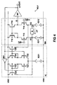
- FIG. 4 An embodiment of such a sense amplifier is shown in Figure 4 illustrates.
- the sense amplifier under consideration is denoted by NLV designated; it contains a differential amplifier NA and one this downstream output driver NT.
- the sense amplifier NLV has like the conventional one described Sense amplifier LV a first input terminal LVIN1, a second input terminal LVIN2, and an output terminal LVOUT on and is designed to do just that in one system containing this to be integrated as in the conventional sense amplifier described above Case and is shown as an example in Figure 2.
- the differential amplifier NA contains a comparison part VT and a current control stage IC.
- the transistor T13 is driven by the voltage U Z ; the gate terminal of transistor T13 is connected to the first input terminal of differential amplifier NA.
- the voltage U Z present at the gate terminal of the transistor T13 makes it more or less highly conductive, as a result of which a current dependent on the voltage U Z flows in the circuit branch containing the transistors T13 and T15.
- the transistor T15 is connected to the transistor T16 to form a current mirror, which causes the same current to flow through the circuit branch containing the transistors T14 and T16 as through the circuit branch containing the transistors T13 and T15. Which current actually flows in the circuit branch containing the transistors T14 and T16 depends on the state of the transistor T14.
- This transistor T14 is driven by the voltage U R ; the gate terminal of transistor T14 is connected to the second input terminal of differential amplifier NA.
- a voltage is established between the transistors T14 and T16, which depends on the ratio of the resistances formed by the transistors T14 and T16.
- This voltage is tapped and output from the differential amplifier NA via the output connection O thereof.
- the signal output from the differential amplifier NA is fed to the output driver NT. This converts the voltage obtained from the differential amplifier NA, depending on its sign and / or size, into a voltage representing level 0 or level 1 and outputs it from the sense amplifier NLV, more precisely from the output terminal LVOUT of the same.
- the voltage output from the output terminal O of the differential amplifier NA and thus also from the output terminal LVOUT of the sense amplifier NLV containing the differential amplifier NA does not signal whether U Z is greater or less than U R , but whether U Z is greater than U R + ⁇ U or less than U R - ⁇ U.
- ⁇ U is the voltage which drops across the resistor R when a current ⁇ I flows through it and is therefore a voltage which corresponds to an offset voltage of the sense amplifier or acts like an offset voltage.
- the size of ⁇ U can be set by the size of the resistor R and by the current ⁇ I flowing through it. In the example under consideration, these variables are defined such that U R + ⁇ U and U R - ⁇ U are only slightly larger than U R. U R + ⁇ U is still significantly lower than the voltage U Z which is fed to the sense amplifier when a programmed memory cell is read out, and U R - ⁇ U is still significantly larger than the voltage U Z which is fed to the sense amplifier when a deleted memory cell is read out.
- the voltage U Z which is fed to the sense amplifier when reading out a memory cell changes with increasing age of the memory device: the voltage U Z which is fed to the sense amplifier when a programmed memory cell is read out can increase with increasing Age of the memory device become smaller, and the voltage U Z , which is supplied to the sense amplifier when an erased memory cell is read out, can increase with increasing age of the memory device. Because ⁇ U is so small, the sense amplifier can still reliably determine the content of a memory cell to be read out. On the other hand, the fact that the sense amplifier U Z no longer compares with U R but with U R + ⁇ U or with U R - ⁇ U can prevent fluctuations in the supply voltage and / or U Z and / or caused by interference.
- the current control stage IC causes the sense amplifier, in the event that its output signal signals that the read-out memory cell has been programmed, to change its output signal only when U Z becomes smaller than U R - ⁇ U, and that the sense amplifier in the event that its output signal signals that the read-out memory cell has been erased, its output signal changes only when U Z becomes greater than U R + ⁇ U. This is particularly important if U Z and U R are relatively close to each other for the above-mentioned or other reasons.
- the transistor T22 conducts and blocks the transistor T21, as a result of which the entire current supplied by the current source IQ21, that is to say through the circuit branch containing the transistors T22 and T24 2 * ⁇ I flows.
- This current is mirrored into the transistor T26 by the current mirror formed by the transistors T24 and T26, so that a current 2 * ⁇ I also flows through it.
- This current is impressed in the node K2 of the comparison part VT.
- the transistor T21 conducts and blocks the transistor T22, as a result of which, through the circuit branch containing the transistors T21 and T23, the entire current supplied by the current source IQ21, that is to say 2 * ⁇ I flows.
- This current is mirrored into the transistor T25 by the current mirror formed by the transistors T23 and T25, so that a current 2 * ⁇ I also flows through it.
- This current is impressed in the node K1 of the comparison part VT.
- This current flow, more precisely the resultant voltage drop .DELTA.U across the resistor R has the effect that the current low level of the signal output from the sense amplifier does not already rise to the high level when the voltage U Z present at the gate terminal of the transistor T13 is the most The gate connection of the transistor T14 exceeds the applied voltage U R , but only when the voltage U Z applied to the gate connection of the transistor T13 exceeds the voltage U R + ⁇ U.
- a sense amplifier constructed as described compares the current or voltage that is supplied to the sense amplifier as an input signal that characterizes the content of the memory cell to be read, depending on the output signal with different threshold values. It compares U Z to U R - ⁇ U when its output signal is high and it compares U Z to U R + ⁇ U when its output signal is low.
- the resistance R by one to replace another element or arrangement which depends on the current from which it flows Voltage drop.
- Such an arrangement exists for example from one or more transistors.
- Differential amplifier could also be provided instead of the one described Differential amplifier a conventional differential amplifier to provide and this one from the output signal of the sense amplifier dependent reference voltage to supply (a supply low reference voltage when the output signal of the sense amplifier has a high level, and a high Supply reference voltage when the output signal of the Sense amplifier has a low level). It would be too conceivable that characterize the content of the memory cell Voltage and / or the supply voltage for the differential amplifier depending on the output signal of the differential amplifier to vary.
Landscapes
- Read Only Memory (AREA)
Applications Claiming Priority (2)
| Application Number | Priority Date | Filing Date | Title |
|---|---|---|---|
| DE10017921A DE10017921A1 (de) | 2000-04-11 | 2000-04-11 | Leseverstärker |
| DE10017921 | 2000-04-11 |
Publications (2)
| Publication Number | Publication Date |
|---|---|
| EP1148509A1 true EP1148509A1 (fr) | 2001-10-24 |
| EP1148509B1 EP1148509B1 (fr) | 2012-02-01 |
Family
ID=7638320
Family Applications (1)
| Application Number | Title | Priority Date | Filing Date |
|---|---|---|---|
| EP01108486A Expired - Lifetime EP1148509B1 (fr) | 2000-04-11 | 2001-04-04 | Amplificateur de lecture |
Country Status (3)
| Country | Link |
|---|---|
| US (1) | US6442091B2 (fr) |
| EP (1) | EP1148509B1 (fr) |
| DE (1) | DE10017921A1 (fr) |
Cited By (1)
| Publication number | Priority date | Publication date | Assignee | Title |
|---|---|---|---|---|
| US7864907B2 (en) | 2006-04-29 | 2011-01-04 | Qimonda Ag | Data receiver with clock recovery circuit |
Families Citing this family (6)
| Publication number | Priority date | Publication date | Assignee | Title |
|---|---|---|---|---|
| ITMI20011231A1 (it) * | 2001-06-12 | 2002-12-12 | St Microelectronics Srl | Circuiteria di rilevamento per la lettura e la verifica del contenutodi celle di memoria non volatili programmabili e cancellabili elettric |
| US7023243B2 (en) | 2002-05-08 | 2006-04-04 | University Of Southern California | Current source evaluation sense-amplifier |
| US6850096B2 (en) * | 2002-05-10 | 2005-02-01 | Yoshio Nishida | Interpolating sense amplifier circuits and methods of operating the same |
| TWI275243B (en) * | 2005-09-14 | 2007-03-01 | Princeton Technology Corp | Voltage controlled amplifier for a signal processing system |
| US10191526B2 (en) * | 2016-11-08 | 2019-01-29 | Qualcomm Incorporated | Apparatus and method for transmitting data signal based on different supply voltages |
| CN108564978B (zh) * | 2018-04-20 | 2021-09-24 | 电子科技大学 | 一种具有冗余结构的读电路 |
Citations (3)
| Publication number | Priority date | Publication date | Assignee | Title |
|---|---|---|---|---|
| EP0491105A1 (fr) * | 1990-12-13 | 1992-06-24 | STMicroelectronics S.r.l. | Circuit de détection amélioré pour dispositifs d'emmagasinages, tels que des mémoires non volatiles, avec discrimination améliorée de détection |
| US5355333A (en) * | 1991-09-26 | 1994-10-11 | Sgs-Thomson Microelectronics, S.R.L. | Dynamic reference system for sense amplifier |
| EP0872850A1 (fr) * | 1997-04-14 | 1998-10-21 | STMicroelectronics S.r.l. | Circuit de lecture analogique de haute précision pour réseaux de mémoire, en particulier pour réseaux de mémoire analogique flash |
Family Cites Families (3)
| Publication number | Priority date | Publication date | Assignee | Title |
|---|---|---|---|---|
| DE69426977T2 (de) * | 1994-05-03 | 2001-07-19 | Stmicroelectronics S.R.L., Agrate Brianza | Abfühlverstärker mit Hysteresis |
| TW404063B (en) * | 1997-02-27 | 2000-09-01 | Toshiba Corp | Semiconductor integrated circuit apparatus and semiconductor memory apparatus |
| JP3690919B2 (ja) * | 1998-07-16 | 2005-08-31 | 富士通株式会社 | メモリデバイス |
-
2000
- 2000-04-11 DE DE10017921A patent/DE10017921A1/de not_active Withdrawn
-
2001
- 2001-04-04 EP EP01108486A patent/EP1148509B1/fr not_active Expired - Lifetime
- 2001-04-11 US US09/833,052 patent/US6442091B2/en not_active Expired - Lifetime
Patent Citations (3)
| Publication number | Priority date | Publication date | Assignee | Title |
|---|---|---|---|---|
| EP0491105A1 (fr) * | 1990-12-13 | 1992-06-24 | STMicroelectronics S.r.l. | Circuit de détection amélioré pour dispositifs d'emmagasinages, tels que des mémoires non volatiles, avec discrimination améliorée de détection |
| US5355333A (en) * | 1991-09-26 | 1994-10-11 | Sgs-Thomson Microelectronics, S.R.L. | Dynamic reference system for sense amplifier |
| EP0872850A1 (fr) * | 1997-04-14 | 1998-10-21 | STMicroelectronics S.r.l. | Circuit de lecture analogique de haute précision pour réseaux de mémoire, en particulier pour réseaux de mémoire analogique flash |
Cited By (1)
| Publication number | Priority date | Publication date | Assignee | Title |
|---|---|---|---|---|
| US7864907B2 (en) | 2006-04-29 | 2011-01-04 | Qimonda Ag | Data receiver with clock recovery circuit |
Also Published As
| Publication number | Publication date |
|---|---|
| EP1148509B1 (fr) | 2012-02-01 |
| DE10017921A1 (de) | 2001-10-18 |
| US20010038564A1 (en) | 2001-11-08 |
| US6442091B2 (en) | 2002-08-27 |
Similar Documents
| Publication | Publication Date | Title |
|---|---|---|
| DE4036973C2 (de) | Schaltung zur Erzeugung einer gegenüber einer extern zugeführten Versorgungsspannung erhöhten Lösch- oder Programmierspannung in einer Halbleiter-Speicherschaltung | |
| DE4224804C1 (de) | Programmierbare logische Schaltungsanordnung | |
| DE69422915T2 (de) | Leseverstärker-organisation | |
| DE3910466C2 (de) | Ausgangspufferschaltung für einen byte-weiten Speicher | |
| DE3340567A1 (de) | Spannungswandlerschaltung | |
| DE3007155C2 (de) | Speichervorrichtung | |
| DE69629669T2 (de) | Leseverfahren und -schaltung für nichtflüchtige Speicherzellen mit Entzerrerschaltung | |
| DE69523547T2 (de) | Einstellbare Stromquelle | |
| DE3249749C2 (fr) | ||
| DE19813707C2 (de) | Spannungspegelumformschaltung | |
| DE2646653C3 (fr) | ||
| DE4201516A1 (de) | Vorrichtung zum automatischen testen eines beanspruchungsbetriebes einer halbleiterspeichervorrichtung | |
| EP1148509B1 (fr) | Amplificateur de lecture | |
| DE60100741T2 (de) | Spannungserhöhung-klemmschaltung für einen flash speicher | |
| DE69226524T2 (de) | Schaltung zur spannungsmessung bei geringer leistung | |
| DE19823687A1 (de) | Fuselatch-Schaltung | |
| DE10120086A1 (de) | Pufferschaltung mit geringem Rauschen | |
| EP0735493A1 (fr) | Circuit d'attaque de bus | |
| EP0748047A1 (fr) | Circuit tampon intégré | |
| DE69323701T2 (de) | Source dekodierter Leseverstärker mit einer speziellen Spaltetreiberspannung | |
| EP1227500B1 (fr) | Circuit de détection de l'état de charge des cellules de mémoire nonvolatiles | |
| DE68923343T2 (de) | NAND Gateschaltungen. | |
| DE69701252T2 (de) | Speicherleseschaltung | |
| DE69520494T2 (de) | Anordnung zur Überwachung einer Schwellspannung | |
| DE69418401T2 (de) | Speicherleseverstärker |
Legal Events
| Date | Code | Title | Description |
|---|---|---|---|
| PUAI | Public reference made under article 153(3) epc to a published international application that has entered the european phase |
Free format text: ORIGINAL CODE: 0009012 |
|
| AK | Designated contracting states |
Kind code of ref document: A1 Designated state(s): AT BE CH CY DE DK ES FI FR GB GR IE IT LI LU MC NL PT SE TR Kind code of ref document: A1 Designated state(s): DE FR IT |
|
| AX | Request for extension of the european patent |
Free format text: AL;LT;LV;MK;RO;SI |
|
| 17P | Request for examination filed |
Effective date: 20020424 |
|
| AKX | Designation fees paid |
Free format text: AT BE CH LI |
|
| RBV | Designated contracting states (corrected) |
Designated state(s): DE FR IT |
|
| REG | Reference to a national code |
Ref country code: DE Ref legal event code: 8566 |
|
| RAP1 | Party data changed (applicant data changed or rights of an application transferred) |
Owner name: INFINEON TECHNOLOGIES AG |
|
| GRAP | Despatch of communication of intention to grant a patent |
Free format text: ORIGINAL CODE: EPIDOSNIGR1 |
|
| GRAS | Grant fee paid |
Free format text: ORIGINAL CODE: EPIDOSNIGR3 |
|
| GRAA | (expected) grant |
Free format text: ORIGINAL CODE: 0009210 |
|
| AK | Designated contracting states |
Kind code of ref document: B1 Designated state(s): DE FR IT |
|
| REG | Reference to a national code |
Ref country code: DE Ref legal event code: R096 Ref document number: 50116045 Country of ref document: DE Effective date: 20120329 |
|
| PG25 | Lapsed in a contracting state [announced via postgrant information from national office to epo] |
Ref country code: IT Free format text: LAPSE BECAUSE OF FAILURE TO SUBMIT A TRANSLATION OF THE DESCRIPTION OR TO PAY THE FEE WITHIN THE PRESCRIBED TIME-LIMIT Effective date: 20120201 |
|
| PLBE | No opposition filed within time limit |
Free format text: ORIGINAL CODE: 0009261 |
|
| STAA | Information on the status of an ep patent application or granted ep patent |
Free format text: STATUS: NO OPPOSITION FILED WITHIN TIME LIMIT |
|
| 26N | No opposition filed |
Effective date: 20121105 |
|
| REG | Reference to a national code |
Ref country code: FR Ref legal event code: ST Effective date: 20121228 |
|
| PG25 | Lapsed in a contracting state [announced via postgrant information from national office to epo] |
Ref country code: FR Free format text: LAPSE BECAUSE OF NON-PAYMENT OF DUE FEES Effective date: 20120430 |
|
| REG | Reference to a national code |
Ref country code: DE Ref legal event code: R097 Ref document number: 50116045 Country of ref document: DE Effective date: 20121105 |
|
| PGFP | Annual fee paid to national office [announced via postgrant information from national office to epo] |
Ref country code: DE Payment date: 20190624 Year of fee payment: 19 |
|
| REG | Reference to a national code |
Ref country code: DE Ref legal event code: R119 Ref document number: 50116045 Country of ref document: DE |
|
| PG25 | Lapsed in a contracting state [announced via postgrant information from national office to epo] |
Ref country code: DE Free format text: LAPSE BECAUSE OF NON-PAYMENT OF DUE FEES Effective date: 20201103 |