EP1148648B1 - Frequenzsynthetisierer - Google Patents
Frequenzsynthetisierer Download PDFInfo
- Publication number
- EP1148648B1 EP1148648B1 EP01101974A EP01101974A EP1148648B1 EP 1148648 B1 EP1148648 B1 EP 1148648B1 EP 01101974 A EP01101974 A EP 01101974A EP 01101974 A EP01101974 A EP 01101974A EP 1148648 B1 EP1148648 B1 EP 1148648B1
- Authority
- EP
- European Patent Office
- Prior art keywords
- output
- clock
- accumulator
- operating
- frequency divider
- Prior art date
- Legal status (The legal status is an assumption and is not a legal conclusion. Google has not performed a legal analysis and makes no representation as to the accuracy of the status listed.)
- Expired - Lifetime
Links
Images


Classifications
-
- H—ELECTRICITY
- H03—ELECTRONIC CIRCUITRY
- H03L—AUTOMATIC CONTROL, STARTING, SYNCHRONISATION OR STABILISATION OF GENERATORS OF ELECTRONIC OSCILLATIONS OR PULSES
- H03L7/00—Automatic control of frequency or phase; Synchronisation
- H03L7/06—Automatic control of frequency or phase; Synchronisation using a reference signal applied to a frequency- or phase-locked loop
- H03L7/16—Indirect frequency synthesis, i.e. generating a desired one of a number of predetermined frequencies using a frequency- or phase-locked loop
- H03L7/18—Indirect frequency synthesis, i.e. generating a desired one of a number of predetermined frequencies using a frequency- or phase-locked loop using a frequency divider or counter in the loop
- H03L7/197—Indirect frequency synthesis, i.e. generating a desired one of a number of predetermined frequencies using a frequency- or phase-locked loop using a frequency divider or counter in the loop a time difference being used for locking the loop, the counter counting between numbers which are variable in time or the frequency divider dividing by a factor variable in time, e.g. for obtaining fractional frequency division
- H03L7/1974—Indirect frequency synthesis, i.e. generating a desired one of a number of predetermined frequencies using a frequency- or phase-locked loop using a frequency divider or counter in the loop a time difference being used for locking the loop, the counter counting between numbers which are variable in time or the frequency divider dividing by a factor variable in time, e.g. for obtaining fractional frequency division for fractional frequency division
- H03L7/1976—Indirect frequency synthesis, i.e. generating a desired one of a number of predetermined frequencies using a frequency- or phase-locked loop using a frequency divider or counter in the loop a time difference being used for locking the loop, the counter counting between numbers which are variable in time or the frequency divider dividing by a factor variable in time, e.g. for obtaining fractional frequency division for fractional frequency division using a phase accumulator for controlling the counter or frequency divider
Definitions
- the present invention relates to a frequency synthesizer device and a mobile radio device using the same and, more particularly, a frequency synthesizer device in which noises in the fractional-N system are reduced and a mobile radio device using the same.
- the frequency synthesizer device is used to produce the carrier wave with any frequency from the reference signal.
- the frequency synthesizer device of high-speed lock up is requested to attain a high C/N and low power consumption in the intermittent reception, etc.
- the setting interval of the output frequency of the voltage-controlled oscillator is limited by the comparison frequency of the phase comparator. In order to obtain the finer setting interval, the comparison frequency must be lowered, so that the lock-up time cannot be shortened.
- the frequency synthesizer device that can reduce the lock-up time there is the frequency synthesizer device that is called the fractional-N system.
- FIG.21 A configuration of the frequency synthesizer device is shown in FIG.21.
- PLL Phase-Locked Loop
- circuit 9 including a phase comparator 1, a low-pass filter (LPF) 2, a voltage-controlled oscillator 3 and a variable frequency divider 4 is provided in the frequency synthesizer device.
- the voltage-controlled oscillator (VCO) 3 is a circuit that oscillates a signal having a frequency in response to an input voltage.
- the variable frequency divider 4 is a circuit that frequency-divides the frequency of the output signal (fvco) of the VCO.
- the phase comparator 1 is a circuit that compares phase of an output signal (fdiv) of the variable frequency divider 4 with phase of the reference signal (fref) to output a phase difference.
- the low-pass filter 2 is a circuit that smoothes an output of the phase comparator 1.
- a frequency-division ratio control circuit 5 is a circuit that controls a frequency-division ratio by using the fdiv as a clock such that the frequency-division ratio is changed in time and a value of its time average contains a value below the decimal point.
- the frequency-division ratio control circuit 5 comprises an accumulator portion 80, a fractional part calculator circuit 70, and a frequency-division ratio adder 6.
- the accumulator portion 80 is a circuit that outputs accumulated results of fractional part data, that are set externally, at a timing of fdiv.
- the fractional part calculator circuit 70 is a circuit that adds output results of the accumulator portion 80 every timing of fdiv.
- the frequency-division ratio adder 6 is a circuit that adds the result calculated by the fractional part calculator circuit 70 and integer part data that are set externally. The added result in the frequency-division ratio adder 6 gives a frequency-division ratio of the variable frequency divider 4.
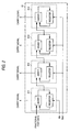
- FIG.22 A configuration of the accumulator portions that are connected in multiple-stage fashion is shown in FIG.22.
- Each of the accumulators 801 to 804 having an adder and a register, and operates by using fdiv as the clock.
- the accumulator 801 at the first stage adds fractional part data that are set by the outside and an output of the register by using the adder, and then updates a value of the register.
- the accumulator 802 at the second stage adds an output of the register and an output of the adder in the accumulator 801 by using the adder, and then updates a value of the register.
- the accumulator 803 and the accumulator 804 perform the same operation as the accumulator 802.
- an adder 701 is a circuit that calculates the fractional part by adding binomial coefficients.
- the delay circuits 702 to 707 are circuits that delay the carry signals of the accumulators to generate sequentially the binomial coefficient represented by the Pascal's triangle.
- the fractional part calculator circuit 70 operates with respect to the carry signals generated from respective accumulators as follows. That is, when the carry signal is input from the accumulator 801, the circuit generates +1. When the carry signal is input from the accumulator 802, the circuit generates +1 and then generates -1 after one clock.
- the circuit When the carry signal is input from the accumulator 803, the circuit generates +1, then generates -2 after one clock, and then generates +1 after two clocks. When the carry signal is input from the accumulator 804, the circuit generates +1, then generates -3 after one clock, then generates +3 after two clocks, and then generates -1 after three clocks. This behavior is shown in a timing chart in FIG. 25.
- the accumulators are operated at the timing of fdiv, and the adders overflows to output the carry signal.
- the delay units that are connected to the carry signals of the accumulator 802, the accumulator 803, and the accumulator 804 delay the carry signal every fdiv period using fdiv as the clock.
- the adder 701 adds the carry signals output at respective stages at the same timing of fdiv and outputs the result.
- the frequency-division ratio adder 6 adds the integer part data that are set externally and the output of the adder 701.
- the result of the adder is the output of the frequency-division ratio control circuit 5 to set the frequency-division ratio of the variable frequency divider 4.
- This frequency-division ratio is changed substantially every timing of fdiv, whereby the frequency component in change of the frequency-division ratio is set high and thus the low frequency component is reduced.
- the change in the frequency-division ratio caused by the carry signals that are generated from the accumulator 802, the accumulator 803, and the accumulator 804 become zero in time average respectively, and it does not affect the average frequency-division ratio. Therefore, only the carry signal generated from the accumulator 801 contributes the average frequency-division ratio.
- US 4,609,881 discloses frequency synthesizers including a variable frequency oscillator which is controlled so as to produce the required synthesised output frequency.
- the variable frequency oscillator forms part of a phase-locked loop which is operative to generate a control signal which adjusts and constrains the oscillator to operate at the correct frequency value.
- the phase-locked loop locks the output signal to a multiple which may be an integer or fractional value of the reference frequency which is generated by stable reference frequency source.
- the output of the oscillator is also fed via a variable ratio frequency divider to one input of a phase comparator where it is compared with the reference frequency from the source.
- any difference in phase or frequency between the two signals which are applied to the phase comparator results in the value of a control signal which is fed via a low pass filter to the variable frequency oscillator.
- the divisor value N of the frequency divider is controlled by an adder which receives from an input interface device information concerning the most signficant bits of the divisor value and the frequency. Information about the fractional part is set to a series of cascaded accumulators. Apart from the first accumulator the remaining accumulators generate a sequence of alternations of the divisor value N in response to a carry signal. To this end each carry signal of the accumulators is fed into a line of delay devices. All carry signals and the outputs of each delay device is fed into an adder.
- EP-0 344 509-A2 discloses a frequency synthesizer with spur compensation.
- the frequency synthesizer comprises the typical elements of a PLL loop specifically a reference oscillator, a phase detector, a low pass filter, a voltage controlled oscillator and a programmable divider.
- a divider control circuit is provided in order to quickly change the devisor value of the divider to provide a fractional frequency synthesizer.
- the divider control circuit comprises a data register forwarding a numerator of an offset value to a multiplexer.
- the offset control circuit determines which of the numerator or offset is forwarded by the multiplexer to a first accumulator.
- the contents of the first accumulator is forwarded to a second accumulator.
- Each of the accumulators generate a single bit carrier signal which influence via a control logic the ratio of a programmable divider.
- a first embodiment of the present invention provides a frequency synthesizer device in which a delay element is provided to the frequency-division ratio control circuit and also an output signal of a variable frequency divider and a delayed signal obtained by delaying the output signal by the delay element are employed as operation clocks of an accumulator portion.
- FIG.1 is a view showing a configuration of the frequency synthesizer device according to the first embodiment of the present invention.
- a PLL (Phase-Locked Loop) circuit including a phase comparator 1, a low-pass filter 2, a voltage-controlled circuit 3, and a variable frequency divider 4 and a frequency-division ratio control circuit 5 are provided.
- the voltage-controlled oscillator 3 is a circuit that oscillates a signal having a frequency in response to an input voltage.
- the variable frequency divider 4 is a circuit that frequency-divides a frequency of an output signal of the voltage-controlled oscillator 3.
- the phase comparator 1 is a circuit that outputs a signal of phase difference between the variable frequency divider 4 and the reference signal to the voltage-controlled oscillator 3 via a low-pass filter 2.
- the frequency-division ratio control circuit 5 is a circuit that controls the variable frequency divider 4 such that a frequency-division ratio of the variable frequency divider 4 is changed in time and a time average value contains a value below the decimal point.
- the frequency-division ratio control circuit 5 comprises a frequency-division ratio adder 6, a fractional part calculator circuit 70, an accumulator portion 81, and a delay element 10.
- the elements other than the accumulator portion 81 and the delay element 10 are similar to those in the background art shown in FIG.21.
- FIG.2 is a view showing a configuration of the accumulator portion 81.
- the accumulator portion 81 includes accumulators 811 to 814. Each accumulator has an adder and a register.
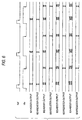
- FIG.3 is a timing chart showing behaviors of change in the operations of the adders and the registers by the clocks in respective accumulators.
- the accumulator 811 at the first stage shown in FIG.2 adds fractional part data that are set by the outside and an output of the register using fdiv as the clock by using the adder, and then updates a value of the register.
- the accumulator 812 at the second stage adds an output of the register using fdiv2 as the clock and an output of the adder in the accumulator 811 by using the adder, and then updates a value of the register.
- the accumulators 813, 814 execute the same operation as the accumulator 812.
- the register in the accumulator 811 updates the data supplied from the adder in synchronism with fdiv.
- the adder executes the operation in respective bits sequentially, and then outputs the carry signal if the carry occurs.
- the adder in the succeeding stage executes the addition when receives change in the output data of the adder at the preceding stage. Since the adding operation is repeated in this manner, the operation time is extended much more at the later stages.
- the register in the accumulator 812 updates the data supplied from the adder in synchronism with fdiv2.
- the accumulators 813, 814 update the data of the register in synchronism with fdiv2, like the accumulator 812. That is, change points of the data in the accumulator are distributed by using fdiv and fdiv2, so that the circuit operation does not concentrate into one timing.
- a one-chip radio portion device can be constructed by integrating the frequency synthesizer device, the transmitter portion, and the receiver portion on the same semiconductor substrate.
- the frequency synthesizer device or the one-chip radio portion device can be mounted on the mobile radio device such as the mobile telephone, etc.
- the delay element is provided to the frequency-division ratio control circuit, and also the output signal of the variable frequency divider and the delayed signal obtained by delaying the output signal are employed as the operation clocks of the accumulator portion. Therefore, the variation in the substrate potential and the variation in the power supply potential generated by the operation of the frequency-division ratio control circuit can be reduced. Also, the degradation of C/N of the frequency synthesizer can be reduced, and also the lock-up time can be reduced. In addition, the power consumption in the intermittent operation can be reduced, and also the influence of the noises upon other blocks constructed on the same substrate can be reduced.
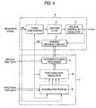
- a second embodiment of the present invention provides a frequency synthesizer device in which the output signal of the variable frequency divider and the reference signal are employed as operation clocks of the accumulator portion.
- FIG.4 is a view showing a configuration of a frequency synthesizer device according to a second embodiment of the present invention.
- a basic configuration of the second embodiment is similar to that of the first embodiment.
- a difference from the first embodiment is that the output fdiv of the variable frequency divider 4 and the reference signal fref are employed as the operation clocks of an accumulator portion 81.
- FIG.5 is a view showing a configuration of the accumulator portion 81.
- the accumulator portion 81 includes accumulators 821 to 824, and each accumulator has the adder and the register.
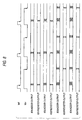
- FIG.6 is a timing chart showing behaviors of change in the operations of the adders and the registers in respective accumulators by the clocks.
- the accumulator 821 at the first stage shown in FIG.5 adds fractional part data that are set by the outside and an output of the register by using the adder, and then updates a value of the register using fref as the clock.
- the accumulator 822 at the second stage adds an output of the register and an output of the adder in the accumulator 821 by using the adder, and then updates a value of the register using fdiv as the clock.
- the accumulators 823, 824 execute the same operation as the accumulator 822.
- Behaviors of change in the operations of the adders and the registers, by the clocks, in the accumulators connected in this manner are shown in a timing chart in FIG.6.
- the register in the accumulator 821 updates the data supplied from the adder in synchronism with fref.
- the adder executes the operation in respective bits sequentially, and then outputs the carry signal if the carry occurs.
- the adder in the succeeding stage executes the addition when receives the data change of the adder at the preceding stage. Since the adding operation is repeated in this manner, the operation time is extended much more at the later stages.
- the register in the accumulator 822 updates the data supplied from the adder in synchronism with fdiv.
- the accumulators 823, 824 update the data of the register in synchronism with fdiv, like the accumulator 822. That is, the change points of the data in the accumulator are distributed by using fref and fdiv, so that the circuit operation does not concentrate into one timing.
- a one-chip radio portion device can be constructed by integrating the frequency synthesizer device, the transmitter portion, and the receiver portion on the same semiconductor substrate.
- the frequency synthesizer device or the one-chip radio portion device can be mounted on the mobile radio device such as the mobile telephone, etc.
- the output signal of the variable frequency divider and the reference signal are employed as operation clocks of the accumulator portion. Therefore, the variation in the substrate potential and the variation in the power supply voltage generated by the operation of the frequency-division ratio control circuit can be reduced. Also, the degradation of C/N of the frequency synthesizer can be reduced, and also the lock-up time can be reduced. In addition, the power consumption in the intermittent operation can be reduced, and also the influence of the noises upon other blocks constructed on the same substrate can be reduced. Furthermore, the delay element can be eliminated by using fref and fdiv as the clocks. Therefore, the optimization of the delay element can also be eliminated, and in addition adjustment in phase displacement between two clock signals due to the variation of the delay element is not needed.
- a third embodiment of the present invention provides a frequency synthesizer device in which the output signal of the variable frequency divider and the reference signal are employed as operation clocks of the accumulator portion, a plurality of accumulators are separated into two half portions in number (almost half the number if the number of the accumulators is the odd number), and the registers in the former half portion are operated by using the reference signal as the clock and the registers in the latter half portion are operated by using the output of the variable frequency divider as the clock.
- FIG. 7 is a view showing a configuration of an accumulator portion 81 of a frequency synthesizer device according to a third embodiment of the present invention.
- the accumulator portion 81 includes accumulators 831 to 834, and each accumulator has the adder and the register.
- a basic configuration of the third embodiment is similar to that of the second embodiment. Adifference from the second embodiment is that the registers in the former half portion of the accumulators are operated by using the reference signal fref as the clock, and the registers in the latter half portion of the accumulators are operated by using the output fdiv of the variable frequency divider 4 as the clock.
- FIG.8 is a timing chart showing behaviors of change in the operations of the adders and the registers in the accumulators by the clocks.
- the operations of elements other than the frequency-division ratio control circuit 5 are similar to the background art shown in FIG.21.
- the output fdiv of the variable frequency divider 4 and the reference signal fref are used as the operation clocks of the accumulator portion 81.
- the registers in the former half portion of the accumulator portion are operated by using the reference signal fref as the clock, and the registers in the latter half portion of the accumulator portion are operated by using the output fdiv of the variable frequency divider 4 as the clock.
- the accumulator 831 at the first stage shown in FIG.7 adds fractional part data that are set by the outside and an output of the register by using the adder, and then updates a value of the register using fref as the clock.
- the accumulator 832 at the second stage adds an output of the register and an output of the adder in the accumulator 831 by using the adder, and then updates a value of the register using fref as the clock.
- the accumulator 833 at the third stage and the accumulator 834 at the fourth stage add an output of the register and an output of the adder in the accumulator at the preceding stage by using the adder and then updates a value of the register using fdiv as the clock respectively.
- the registers in the accumulators 833, 834 update the data supplied from the adders in synchronism with fdiv. That is, the change points of the data in the accumulators are distributed by using fref and fdiv, so that the circuit operation does not concentrate into one timing. In particular, since fref and fdiv are separately used by the former and latter half portions of the accumulators, the circuit number of the accumulators that includes plural stages and are simultaneously operated can be minimized.
- a one-chip radio portion device can be constructed by integrating the frequency synthesizer device, the transmitter portion, and the receiver portion on the same semiconductor substrate.
- the frequency synthesizer device or the one-chip radio portion device can be installed on the mobile radio device such as the mobile telephone, etc.
- the output signal of the variable frequency divider and the reference signal are employed as operation clocks of the accumulator portion, a plurality of accumulators are separated into two half portions in number (almost half the number if the number of the accumulators is the odd number), and the registers in the former half portion are operated by using the reference signal as the clock and also the registers in the latter half portion are operated by using the output of the variable frequency divider as the clock. Therefore, the variation in the substrate potential and the variation in the power supply voltage generated by the operation of the frequency-division ratio control circuit can be reduced. Also, the degradation of C/N of the frequency synthesizer can be reduced, and also the lock-uptime canbe reduced.
- the power consumption in the intermittent operation can be reduced, and also the influence of the noises upon other blocks constructed on the same substrate can be reduced. Furthermore, since fref and fdiv are used separately by the former and latter half portions of the accumulators, the operation noises of the accumulators can be reduced rather than those in the first and second embodiments.
- a fourth embodiment of the present invention provides a frequency synthesizer device in which the delay element is provided to the frequency-division ratio control circuit, the output signal of the variable frequency divider and the delayed signal of the output signal are employed as operation clocks of the accumulator portion, and a plurality of accumulators are connected to the accumulators in the succeeding stages via the outputs of the registers in respective stages.
- FIG.9 is a view showing a configuration of an accumulator portion 81 of a frequency synthesizer device according to a fourth embodiment of the present invention.
- the accumulator portion 81 includes accumulators 841 to 844, and each accumulator has the adder and the register.
- a basic configuration of the fourth embodiment is similar to that of the first embodiment.
- a difference from the first embodiment is configurations of the accumulator portion 81 and the fractional part calculator circuit 70.
- FIG.10 is a timing chart showing behaviors of change in the operations of the adders and the registers in the accumulators by the clocks.
- FIG.11 is a view showing a configuration of the fractional part calculator circuit 70.
- an adder 701 is a circuit that detects the fractional part by calculating the binomial coefficient.
- Delay circuits 702 to 707, 711 to 716 are circuits that generates the binomial coefficient, that is represented by the Pascal's triangle, sequentially by delaying the carry signal of the accumulator.
- the accumulator 841 at the first stage shown in FIG.9 adds fractional part data that are set by the outside and an output of the register by using the adder, and then updates a value of the register using fdiv as the clock.
- the accumulator 842 at the second stage adds an output of the register and an output of the register in the accumulator 841 by using the adder, and then updates a value of the register using fdiv2 as the clock.
- the accumulators 843, 844 execute the same operation as the accumulator 842.
- the register in the accumulator 841 updates the data supplied from the adder in synchronism with fdiv.
- the adder executes the operation in respective bits sequentially, and then outputs the carry signal if the carry occurs.
- the adder in the succeeding stage executes the operation when receives the data of the register at the preceding stage, that are changed at the timing of fdiv.
- the register in the accumulator 842 updates the data supplied from the adder in synchronism with fdiv2.
- the accumulators 843, 844 update the data of the register in synchronism with fdiv2, like the accumulator 842. That is, the change points of the data in the accumulator are distributed by using fdiv and fdiv2, so that the circuit operation does not concentrate into one timing.
- FIG.11 is a view showing a configuration of the fractional part calculator circuit 70.
- delay circuits 711 to 716 are provided. These delay circuits are needed to match respective timings of the addition because respective stages are connected to the succeeding stages via the register in configuration of the accumulator portion. This behavior is shown in a timing chart of FIG.12.
- the accumulator at the first stage delays the signal by three clocks using fdiv2 until the calculated result is transmitted to the fourth stage after such calculated result is input into the succeeding stage by fdiv2.
- the accumulator at the second stage delays the signal by two clocks using fdiv, and the accumulator at the third stage delays the signal by one clock using fdiv. Accordingly, the calculated result of the accumulator can be transmitted precisely to the adder 701 at the timing of fdiv.
- a one-chip radio portion device can be constructed by integrating the frequency synthesizer device, the transmitter portion, and the receiver portion on the same semiconductor substrate.
- the frequency synthesizer device or the one-chip radio portion device can be installed on the mobile radio device such as the mobile telephone, etc.
- the delay element is provided to the frequency-division ratio control circuit, and also the output signal of the variable frequency divider and the delayed signal of the output signal are employed as operation clocks of the accumulator portion. Therefore, the variation in the substrate potential and the variation in the power supply voltage generated by the operation of the frequency-division ratio control circuit can be reduced. Also, the degradation of C/N of the frequency synthesizer can be reduced, and also the lock-up time can be reduced. In addition, the power consumption in the intermittent operation can be reduced, and also the influence of the noises upon other blocks constructed on the same substrate can be reduced.
- a plurality of accumulators are connected to the accumulators in the succeeding stages via the outputs of the registers in respective stages. Therefore, the calculated result of the adder is never transmitted sequentially to the adder in the accumulator at the succeeding stage to thus reduce the overall circuit operation time, and therefore the noise reducing effect can be achieved rather than the first embodiment.
- a fifth embodiment of the present invention provides a frequency synthesizer device in which the output signal of the variable frequency divider and the reference signal are employed as operation clocks of the accumulator portion, a plurality of accumulators are separated into two half portions in number (almost half the number if the number of the accumulators is the odd number), the registers at the odd-numbered stages are operated by using the reference signal as the clock and the registers at the even-numbered stages are operated by using the output of the variable frequency divider as the clock, and a plurality of accumulators are connected to the accumulators in the succeeding stages via the outputs of the registers in respective stages.
- FIG.13 is a view showing a configuration of a frequency synthesizer device according to a fifth embodiment of the present invention.
- a configuration of the accumulator portion 81, a configuration of the fractional part calculator circuit 71, and the use of two signals fdiv and fref as the clocks are different from the configuration in the fourth embodiment.
- FIG. 14 is a view showing a configuration of the accumulator portion 81.
- the accumulator portion 81 includes accumulators 851 to 854, and each accumulator has the adder and the register.
- FIG.15 is a timing chart showing behaviors of change in the operations of the adders and the registers in the accumulators by the clocks.
- FIG.16 is a functional block diagram of the fractional part calculator circuit 71.
- the accumulator 851 at the first stage adds fractional part data that are set by the outside and an output of the register by using the adder, and then updates a value of the register using fref as the clock.
- the accumulator 852 at the second stage adds an output of the register and an output of the resister in the accumulator 851 by using the adder, and then updates a value of the register using fdiv as the clock.
- the accumulator 853 at the third stage adds an output of the register and an output of the register in the accumulator 852 by using the adder, and then updates a value of the register using fref as the clock.
- the accumulator 854 at the fourth stage adds an output of the register and an output of the register in the accumulator 853 by using the adder, and then updates a value of the register using fdiv as the clock.
- Behaviors of change in the operations of the adders and the registers, by the clocks, in the accumulators connected in this manner are shown in a timing chart in FIG.15.
- the registers in the accumulator 851 and the accumulator 853 update the data supplied from the adders in synchronism with fref.
- the adders execute the operation in respective bits in sequence, and then outputs the carry signal if the carry occurs.
- the registers in the accumulator 852 and the accumulator 854 update the data supplied from the adders in synchronism with fdiv.
- the adders execute the operation in respective bits in sequence, and then outputs the carry signal if the carry occurs. That is, the change points of the data in the accumulator are distributed by using fref and fdiv, so that the circuit operation does not concentrate into one timing.
- FIG. 16 is a functional block diagram of a fractional part calculator circuit 71.
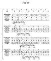
- a difference from the configuration in the fourth embodiment is that a delay circuit 721 and a delay circuit 722 are provided. These delay circuits are needed to match respective timings of the addition because clock timings of the accumulator portion are changed. This behavior is shown in a timing chart of FIG.17.
- the calculated result of the accumulator at the first stage is delayed by 2.5 clocks using fdiv
- the calculated result of the accumulator at the second stage is delayed by 1.5 clocks using fdiv
- the calculated result of the accumulator at the third stage is delayed by 0.5 clock using fref and by 0.5 clock using fdiv
- the calculated result of the accumulator at the fourth stage is delayed by 0.5 clock using fdiv. Accordingly, the calculated result of the accumulator can be transmitted precisely to the adder 701 at the timing of fdiv.
- a one-chip radio portion device can be constructed by integrating the frequency synthesizer device, the transmitter portion, and the receiver portion on the same semiconductor substrate.
- the frequency synthesizer device or the one-chip radio portion device can be installed on the mobile radio device such as the mobile telephone, etc.
- the output signal of the variable frequency divider and the reference signal are employed as operation clocks of the accumulator portion, a plurality of accumulators are separated into two half portions in number (almost half the number if the number of the accumulators is the odd number), the registers at the odd-numbered stages are operated by using the reference signal as the clock and the registers at the even-numbered stages are operated by using the output of the variable frequency divider as the clock. Therefore, the variation in the substrate potential and the variation in the power supply voltage generated by the operation of the frequency-division ratio control circuit can be reduced. Also, the degradation of C/N of the frequency synthesizer can be reduced, and also the lock-up time canbe reduced.
- the power consumption in the intermittent operation can be reduced, and also the influence of the noises upon other blocks constructed on the same substrate can be reduced.
- the delay element used in the fourth embodiment is not needed by using fref and fdiv as the clock. Therefore, the optimization of the delay element and phase adjustment between two clock signals due to variation can be eliminated.
- a sixth embodiment of the present invention provides a frequency synthesizer device in which the output signal of the variable frequency divider and the reference signal are employed as operation clocks of the accumulator portion, and a plurality of accumulators are connected to the succeeding stages via the outputs of the registers in respective stages.
- a difference from the fourth embodiment is a configuration of an accumulator portion 81.
- FIG.18 is a view showing the configuration of the accumulator portion 81.
- the accumulator portion 81 includes accumulators 861 to 864, and each accumulator has the adder and the register.
- the accumulator 861 at the first stage adds fractional part data that are set by the outside and an output of the register by using the adder, and then updates a value of the register using fref as the clock.
- the accumulator 862 at the second stage adds an output of the register and an output of the register in the accumulator 861 by using the adder, and then updates a value of the register using fdiv as the clock.
- the accumulators 863, 864 execute the similar operation to the accumulator 862.
- the register in the accumulator 861 updates the data supplied from the adder in synchronism with fref.
- the adder executes the operation in respective bits in sequence, and then outputs the carry signal if the carry occurs.
- the adder in the succeeding stage executes the operation when it receives the change in the data.
- the register in the accumulator 862 updates the data supplied from the adder in synchronism with fdiv.
- the accumulator 863 and the accumulator 864 update the data of the register in synchronism with fdiv, like the accumulator 862. That is, the change points of the data in the accumulator are distributed by using fref and fdiv, so that the circuit operation does not concentrate into one timing.
- a one-chip radio portion device can be constructed by integrating the frequency synthesizer device, the transmitter portion, and the receiver portion on the same semiconductor substrate.
- the frequency synthesizer device or the one-chip radio portion device can be installed on the mobile radio device such as the mobile telephone, etc.
- the output signal of the variable frequency divider and the reference signal are employed as operation clocks of the accumulator portion. Therefore, the variation in the substrate potential and the variation in the power supply voltage generated by the operation of the frequency-division ratio control circuit can be reduced. Also, the degradation of C/N of the frequency synthesizer can be reduced, and also the lock-up time can be reduced. In addition, the power consumption in the intermittent operation can be reduced, and also the influence of the noises upon other blocks constructed on the same substrate can be reduced. Furthermore, the delay element used in the fourth embodiment is not needed by using fref and fdiv as the clock. Therefore, the optimization of the delay element and phase adjustment between two clock signals due to variation can be eliminated. Besides, the overlapped operations between the data update of the register and the data update of the register in the preceding stage can be reduced in operation of the adders, and therefore the noise reducing effect can be achieved rather than the fifth embodiment.
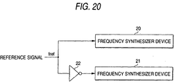
- a seventh embodiment of the present invention provides a plurality of frequency synthesizer devices in which reference signals that have different phase respectively are distributed to a plurality of accumulators in the frequency synthesizer devices, that are operated at a different clock timing respectively.
- FIG.20 is a functional block diagram of a plurality of frequency synthesizer devices according to the seventh embodiment of the present invention.
- references 20 and 21 denote any frequency synthesizer device shown in the first to sixth embodiments.
- An inverter 22 is a circuit that changes the phase of the reference signal.
- the reference signal is input into the frequency synthesizer device 20 without change of phase as it is.
- a secondary reference signal which is obtained by inverting the phase of the reference signal by using the inverter 22 is input into the frequency synthesizer device 21.
- a one-chip radio portion device can be constructed by integrating the frequency synthesizer device, the transmitter portion, and the receiver portion on the same semiconductor substrate.
- the frequency synthesizer device or the one-chip radio portion device can be installed on the mobile radio device such as the mobile telephone, etc.
- the reference signals are used while changing their phases respectively. Therefore, the variation in the substrate potential and the variation in the power supply voltage generated by the operation of the frequency-division ratio control circuit can be reduced. Also, the degradation of C/N of the frequency synthesizer can be reduced, and also the lock-up time can be reduced. In addition, the power consumption in the intermittent operation can be reduced, and also the influence of the noises upon other blocks constructed on the same substrate can be reduced.
- a frequency synthesizer device comprising: a PLL circuit that includes a reference signal inputting means, a phase comparator, a low-pass filter, a voltage-controlled oscillator, and a variable frequency divider; and a frequency-division ratio control circuit including a plurality of accumulators for controlling the variable frequency divider such that a frequency division ratio of the variable frequency divider is changed in time and a time average value of the frequency division ratio contains a value below a decimal point and each having a register and an adder, a fractional part calculator circuit for receiving a carry signal generated by the adder to add binomial coefficients in sequence, and a frequency-division ratio adder for adding an output of the fractional part calculator circuit and integer part data to set the frequency division ratio in the variable frequency divider, wherein the frequency-division ratio control circuit is operated at a plurality of clocks having different timings, whereby a signal having a frequency that is equal to
Landscapes
- Stabilization Of Oscillater, Synchronisation, Frequency Synthesizers (AREA)
Claims (19)
- Frequenzsynthesizervorrichtung, die aufweist:wobei die Frequenz-Teilungsverhältnis-Steuerschaltung (5) an einer Mehrzahl von Takten (fdiv, fref), die unterschiedliche Zeitabstimmungen haben, betrieben wird,eine PLL-Schaltung (9), umfassend eine Referenzsignal-Eingabeeinrichtung, einen Phasenkomparator (1), einen Tiefpassfilter (2), einen spannungsgesteuerten Oszillator (3) und einen variablen Frequenzteiler (4); undeine Frequenz-Teilungsverhältnis-Steuerschaltung (5) zum Steuern des variablen Frequenzteilers so, dass ein Frequenz-Teilungsverhältnis des variablen Frequenzteilers in der Zeit geändert wird und ein Zeitmittelungswert des Frequenz-Teilungsverhältnisses einen Wert unterhalb eines Dezimalpunkts enthält, mit:einer Mehrzahl von Akkumulatoren, von denen jeder ein Register (811, 812, 813, 814; 821, 822, 823, 824; 831, 832, 833, 834; 841, 842, 843, 844; 851, 852, 853, 854; 861, 862, 863, 864) und einen Addierer besitzt;eine Eingabeeinrichtung, um Bruchteildaten in den Akkumulator (811, 821, 831, 841, 851, 861) an einer ersten Stufe einzugeben;eine Bruchteilkalkulatorschaltung (70) zum Aufnehmen eines Trägersignals, erzeugt durch den Addierer, um binomische Koeffizienten in Folge zu addieren; undeinen Frequenz-Teilungsverhältnis-Addierer (6) zum Addieren eines Ausgangs der Bruchteilkalkulatorschaltung und der ganzteiligen Daten, um das Frequenz-Teilungsverhältnis in dem variablen Frequenzteiler einzustellen,
wodurch ein Signal, das eine Frequenz besitzt, die gleich zu einem Produkt des in der Zeit gemittelten Werts des Frequenz-Teilungsverhältnisses und einer Frequenz eines Referenzsignals ist, erzeugt wird. - Frequenzsynthesizervorrichtung nach Anspruch 1, wobei die Frequenz-Teilungsverhältnis-Steuerschaltung (5) weiterhin umfasst:eine Einrichtung zum Betreiben des Registers eines Akkumulators (811) an einer ersten Stufe unter Verwendung eines Ausgangs des variablen Frequenzteilers (fdiv) als einen Takt;eine Verzögerungsvorrichtung (10) zum Betreiben von Registern von Akkumulatoren (812, 813, 814) an einer zweiten und darauffolgenden Stufe(n) unter Verwendung eines verzögerten Signals (fdiv2) des Ausgangs des variablen Frequenzteilers als den Takt;einen Verbinder, um einen Ausgang des Addierers als einen Eingang des Akkumulators an einer darauffolgenden Stufe (812) zuzuführen; undeine Einrichtung, um das Trägersignal länger als das Trägersignal an einer vorhergehenden Stufe um einen Takt unter Verwendung einer Verzögerungsschaltung (D) der Bruchteilkalkulatorschaltung (70), die unter Verwendung des Ausgangs des variablen Frequenzteilers als der Takt arbeitet, zu verzögern.
- Frequenzsynthesizervorrichtung nach Anspruch 1, wobei die Frequenz-Teilungsverhältnis-Steuerschaltung (15) weiterhin umfasst:eine Einrichtung zum Betreiben des Registers eines Akkumulators an einer ersten Stufe (821; 841; 861) unter Verwendung des Referenzsignals (fref) als einen Takt;eine Einrichtung zum Betreiben von Registern von Akkumulatoren (822, 823, 824; 842, 843, 844; 862, 863, 864) an einer zweiten und darauffolgenden Stufe(n) unter Verwendung eines Ausgangs des variablen Frequenzteilers als den Takt;einen Verbinder zum Zuführen eines Ausgangs des Addierers als einen Eingang des Akkumulators an einer darauffolgenden Stufe; undeine Einrichtung, um das Trägersignal länger als das Trägersignal an einer vorhergehenden Stufe um einen Takt unter Verwendung einer Verzögerungsschaltung (D) der Bruchteilkalkulatorschaltung, die unter Verwendung des Ausgangs des variablen Frequenzteilers als den Takt arbeitet, zu verzögern.
- Frequenzsynthesizervorrichtung nach Anspruch 1, wobei die Frequenz-Teilungsverhältnis-Steuerschaltung (5) weiterhin umfasst:eine Einrichtung zum Betreiben von Registern der Akkumulatoren (831, 832) der ersteren Hälfte unter Verwendung des Referenzsignals (fref) als einen Takt;eine Einrichtung zum Betreiben von Registern von Akkumulatoren (833, 834) der letzteren Hälfte unter Verwendung eines Ausgangs des variablen Frequenzteilers (fdiv) als den Takt;einen Verbinder zum Zuführen eines Ausgangs des Addierers als einen Eingang des Akkumulators an einer darauffolgenden Stufe; undeine Einrichtung zum Verzögern des Trägersignals länger als das Trägersignal an einer vorhergehenden Stufe um einen Takt unter Verwendung einer Verzögerungsschaltung (D) der Bruchteilkalkulatorschaltung, die unter Verwendung des Ausgangs des variablen Frequenzteilers als den Takt arbeitet.
- Frequenzsynthesizervorrichtung nach Anspruch 1, wobei die Frequenz-Teilungsverhältnis-Steuerschaltung (5) weiterhin umfasst:eine Einrichtung zum Betreiben des Registers eines Akkumulators (841) an einer ersten Stufe unter Verwendung eines Ausgangs des variablen Frequenzteilers (fdiv) als einen Takt;eine Verzögerungsvorrichtung zum Betreiben von Registern von Akkumulatoren (842, 843, 844) an einer zweiten und darauffolgenden Stufe unter Verwendung eines verzögerten Signals (fdiv2) des Ausgangs des variablen Frequenzteilers als den Takt;einen Verbinder zum Zuführen eines Ausgangs des Registers als einen Eingang des Akkumulators an einer darauffolgenden Stufe (842); undeine Einrichtung zum Verzögern aller Trägersignale um denselben Betrag unter Verwendung einer Verzögerungsschaltung der Bruchteilkalkulatorschaltung (D), die unter Verwendung des Ausgangs des variablen Frequenzteilers als den Takt arbeitet.
- Frequenzsynthesizervorrichtung nach Anspruch 1, wobei die Frequenz-Teilungsverhältnis-Steuerschaltung (5) weiterhin umfasst:eine Einrichtung zum Betreiben von Registern von Akkumulatoren (851, 853) an ungerade nummerierten Stufen unter Verwendung des Referenzsignals (fref) als einen Takt;eine Einrichtung zum Betreiben von Registern von Akkumulatoren (852, 854) an gerade nummerierten Stufen unter Verwendung eines Ausgangs eines variablen Frequenzteilers (fdiv) als den Takt;einen Verbinder zum Zuführen eines Ausgangs des Registers als einen Eingang des Akkumulators an einer darauffolgenden Stufe; undeine Einrichtung zum passenden Addieren von Zeitabstimmungen des Trägersignals unter Verwendung einer Verzögerungsschaltung (721, 722) der Bruchteilkalkulatorschaltung (70), die unter Verwendung von zwei Typen von Takten des Referenzsignals und des Ausgangs des variablen Frequenzteilers arbeitet.
- Frequenzsynthesizervorrichtung nach Anspruch 1, wobei die Frequenz-Teilungsverhältnis-Steuerschaltung (5) weiterhin umfasst:eine Einrichtung zum Betreiben des Registers eines Akkumulators (821; 841; 861) an einer ersten Stufe unter Verwendung des Referenzsignals (fref) als einen Takt;eine Einrichtung, um zu bewirken, dass Register von Akkumulatoren (822, 823, 824; 842, 843, 844; 862, 863, 864) an einer zweiten und darauffolgenden Stufe(n) unter Verwendung eines Ausgangs des variablen Frequenzteilers (fdiv) als den Takt zu arbeiten;einen Verbinder zum Zuführen eines Ausgangs des Registers als einen Eingang des Akkumulators an einer darauffolgenden Stufe; undeine Einrichtung (D) zum Verzögern aller Trägersignale um denselben Betrag unter Verwendung einer Verzögerungsschaltung (702-707, 711-716) der Bruchteilkalkulatorschaltung, die unter Verwendung des Ausgangs des variablen Frequenzteilers als den Takt arbeitet.
- Frequenzsynthesizervorrichtung, die aufweist:eine Mehrzahl von Frequenzsynthesizern gemäß Anspruch 1; undeine Einrichtung zum Erzeugen sekundärer Referenzsignale, die eine unterschiedliche Phase gegenüber einem gemeinsamen Referenzsignal haben und die sekundären Referenzsignale verteilen.
- Funkbereichsvorrichtung, die aufweist:wobei der Senderbereich und der Empfängerbereich und die Frequenzsynthesizervorrichtung auf demselben Halbleitersubstrat integriert sind.Frequenzsynthesizervorrichtungen nach Anspruch 1; undeinen Senderbereich und einen Empfängerbereich;
- Mobile Funkvorrichtung, die Frequenzsynthesizervorrichtungen nach Anspruch 1 aufweist.
- Mobile Funkvorrichtung, die eine Funkbereichsvorrichtungen nach Anspruch 9 aufweist.
- Verfahren zum Betreiben einer Frequenzsynthesizervorrichtung, das die Schritte aufweist:wobei die Akkumulatoren (811-814; 821-824; 831-834; 841-844; 851-854; 861-864) unter Takten betrieben werden, die unterschiedliche Zeitabstimmungen haben.Eingeben von Bruchteildaten in einen Akkumulator (811, 821, 831, 841, 851, 861) an einer ersten Stufe in einer Frequenz-Teilungsverhältnis-Steuerschaltung (5), die einen variablen Frequenzteiler (4) in einer PLL-Schaltung (9), umfassend eine Referenzsignaleingabeeinrichtung, einen Phasenkomparator (1), einen Tiefpassfilter (2), einen spannungsgesteuerten Oszillator (3) und den Dividierer (4) mit variabler Frequenz steuert;Erzeugen eines Trägersignals durch Addieren der Bruchteildaten unter Verwendung von Akkumulatoren (811-814; 821-824; 831-834; 841-844; 851-854; 861-864) an jeweiligen Stufen in Folge;Berechnen eines Bruchteils durch Erzeugen von binomischen Koeffizienten in Folge basierend auf dem Trägersignal und Addieren der binomischen Koeffizienten;Berechnen eines Frequenz-Teilungsverhältnisses, dessen Zeitmittelwert in der Zeit geändert wird, um einen Wert unterhalb eines Dezimalpunkts durch Addieren von Ganzteildaten zu dem Bruchteil, Einstellen des Frequenz-Teilungsverhältnisses in dem variablen Frequenzteiler, zu erhalten; undErzeugen eines Signals, das eine Frequenz besitzt, die gleich zu einem Produkt des in der Zeit gemittelten Werts und einer Frequenz eines Referenzsignals ist,
- Verfahren zum Betreiben einer Frequenzsynthesizervorrichtung nach Anspruch 12, das weiterhin die Schritte umfasst:Betreiben des Registers eines Akkumulators an einer ersten Stufe (811) unter Verwendung eines Ausgangs des variablen Frequenzteilers (fdiv) als einen Takt;Betreiben von Registern von Akkumulatoren an einer zweiten und darauffolgenden Stufe(n) (812, 813, 814) unter Verwendung eines verzögerten Signals (fdiv2) des Ausgangs des Dividierers mit variabler Frequenz als den Takt;Addieren eines Ausgangs des Addierers in dem Akkumulator an einer darauffolgenden Stufe zu einem Ausgang des Registers; undVerzögern des Trägersignals länger als das Trägersignal an einer vorhergehenden Stufe um einen Takt durch Betreiben einer Verzögerungsschaltung (D) der Bruchteilkalkulatorschaltung (70) unter Verwendung des Ausgangs des variablen Frequenzteilers (fdiv) als den Takt.
- Verfahren zum Betreiben einer Frequenzsynthesizervorrichtung nach Anspruch 12, das weiterhin die Schritte aufweist:Betreiben des Registers eines Akkumulators an einer ersten Stufe (821, 849, 861) unter Verwendung des Referenzsignals (fref) als einen Takt;Betreiben von Registern von Akkumulatoren an einer zweiten und darauffolgenden Stufe(n) (822, 823, 824; 842, 843, 844; 862, 863, 864) unter Verwendung eines Ausgangs des variablen Frequenzteilers (fdiv) als den Takt;Addieren eines Ausgangs des Addierers in dem Akkumulator an einer darauffolgenden Stufe zu einem Ausgang des Registers; undVerzögern des Trägersignals länger als das Trägersignal an einer vorhergehenden Stufe um einen Takt durch Betreiben einer Verzögerungsschaltung (D) der Bruchteilkalkulatorschaltung unter Verwendung des Ausgangs des variablen Frequenzteilers als den Takt.
- Verfahren zum Betreiben einer Frequenzsynthesizervorrichtung nach Anspruch 12, das weiterhin die Schritte aufweist:Betreiben von Registern der ersteren Hälfte von Akkumulatoren (831, 832) unter Verwendung des Referenzsignals (fref) als einen Takt;Betreiben von Registern der letzteren Hälfte von Akkumulatoren (833, 834) unter Verwendung eines Ausgangs des variablen Frequenzteilers (fdiv) als den Takt; Addieren eines Ausgangs des Addierers in dem Akkumulator an einer darauffolgenden Stufe zu einem Ausgang des Registers; undVerzögern des Trägersignals länger als das Trägersignal an einer vorhergehenden Stufe um einen Takt durch Betreiben einer Verzögerungsschaltung (D) der Bruchteilkalkulatorschaltung (70) unter Verwendung des Ausgangs des variablen Frequenzteilers (fdiv) als den Takt.
- Verfahren zum Betreiben einer Frequenzsynthesizervorrichtung nach Anspruch 12, das weiterhin die Schritte aufweist:Betreiben eines Registers eines Akkumulators (841) an einer ersten Stufe unter Verwendung eines Ausgangs des variablen Frequenzteilers (fdiv) als einen Takt;Betreiben von Registern von Akkumulatoren (842, 843, 844) an einer zweiten und darauffolgenden Stufe(n) unter Verwendung eines verzögerten Signals (fdiv2) des Ausgangs des Dividierers mit variabler Frequenz als den Takt;Addieren eines Ausgangs des Registers in dem Akkumulator an einer darauffolgenden Stufe zu einem Ausgang des Registers; undVerzögern aller Trägersignale um einen selben Betrag durch Betreiben einer Verzögerungsschaltung (D) der Bruchteilkalkulatorschaltung unter Verwendung des Ausgangs des variablen Frequenzteilers als den Takt.
- Verfahren zum Betreiben einer Frequenzsynthesizervorrichtung nach Anspruch 12, das weiterhin die Schritte aufweist:Betreiben von Registern von Akkumulatoren (851, 853) an ungerade nummerierten Stufen unter Verwendung des Referenzsignals (fref) als einen Takt;Betreiben von Registern von Akkumulatoren (852, 854) an gerade nummerierten Stufen unter Verwendung eines Ausgangs des variablen Frequenzteilers (fdiv) als den Takt;Addieren eines Ausgangs des Registers in dem Akkumulator an einer darauffolgenden Stufe zu einem Ausgang des Registers; undAnpassen von Additionszeitabstimmungen des Trägersignals durch Betreiben einer Verzögerungsschaltung (D) der Bruchteilkalkulatorschaltung unter Verwendung von Zwei-Typ-Takten des Referenzsignals und des Ausgangs des variablen Frequenzteilers.
- Verfahren zum Betreiben einer Frequenzsynthesizervorrichtung nach Anspruch 12, das weiterhin die Schritte aufweist:Betreiben des Registers eines Akkumulators (821; 841; 861) an einer ersten Stufe unter Verwendung des Referenzsignals (fref) als einen Takt;Betreiben von Registern von Akkumulatoren an einer zweiten und darauffolgenden Stufe(n) (822, 823, 824; 842, 843, 844; 862, 863, 864) unter Verwendung eines Ausgangs des variablen Frequenzteilers (fdiv) als den Takt;Addieren eines Ausgangs des Registers in dem Akkumulator an einer darauffolgenden Stufe zu einem Ausgang des Registers; undVerzögern aller Trägersignale um einen selben Betrag durch Betreiben einer Verzögerungsschaltung (702-707; 711-716) der Bruchteilkalkulatorschaltung (70) unter Verwendung des Ausgangs des variablen Frequenzteilers als den Takt.
- Verfahren zum Betreiben einer Frequenzsynthesizervorrichtung, das die Schritte aufweist:Erzeugen eines Referenzsignals (fref);Erzeugen einer Mehrzahl von sekundären Referenzsignalen, die eine unterschiedliche Phase gegenüber dem Referenzsignal haben; undVerteilen der sekundären Referenzsignale zu einer Mehrzahl von Frequenzsynthesizervorrichtungen, wobei jede ein Verfahren nach Anspruch 12 durchführt.
Applications Claiming Priority (2)
| Application Number | Priority Date | Filing Date | Title |
|---|---|---|---|
| JP2000115190 | 2000-04-17 | ||
| JP2000115190A JP2001298363A (ja) | 2000-04-17 | 2000-04-17 | 周波数シンセサイザ装置とそれを用いた移動無線機 |
Publications (2)
| Publication Number | Publication Date |
|---|---|
| EP1148648A1 EP1148648A1 (de) | 2001-10-24 |
| EP1148648B1 true EP1148648B1 (de) | 2004-08-11 |
Family
ID=18626884
Family Applications (1)
| Application Number | Title | Priority Date | Filing Date |
|---|---|---|---|
| EP01101974A Expired - Lifetime EP1148648B1 (de) | 2000-04-17 | 2001-01-29 | Frequenzsynthetisierer |
Country Status (5)
| Country | Link |
|---|---|
| US (1) | US6728526B2 (de) |
| EP (1) | EP1148648B1 (de) |
| JP (1) | JP2001298363A (de) |
| CN (1) | CN1199355C (de) |
| DE (1) | DE60104761T2 (de) |
Families Citing this family (31)
| Publication number | Priority date | Publication date | Assignee | Title |
|---|---|---|---|---|
| US8385476B2 (en) | 2001-04-25 | 2013-02-26 | Texas Instruments Incorporated | Digital phase locked loop |
| JP4828730B2 (ja) * | 2001-07-05 | 2011-11-30 | 富士通株式会社 | 伝送装置 |
| JP3612506B2 (ja) * | 2001-09-04 | 2005-01-19 | Necアクセステクニカ株式会社 | 移動携帯端末装置 |
| AU2002363140A1 (en) * | 2001-10-31 | 2003-05-12 | Sirf Technologies, Inc. | Fractional-r- frequency synthesizer |
| US6707855B2 (en) * | 2002-06-20 | 2004-03-16 | Nokia Corporation | Digital delta sigma modulator in a fractional-N frequency synthesizer |
| US7024171B2 (en) * | 2003-02-25 | 2006-04-04 | Icom America, Incorporated | Fractional-N frequency synthesizer with cascaded sigma-delta converters |
| US7339861B2 (en) * | 2003-04-21 | 2008-03-04 | Matsushita Electric Industrial Co., Ltd. | PLL clock generator, optical disc drive and method for controlling PLL clock generator |
| JP4434825B2 (ja) * | 2003-05-08 | 2010-03-17 | パナソニック株式会社 | インパルス波形生成装置 |
| US6919744B2 (en) * | 2003-08-20 | 2005-07-19 | Agere Systems Inc. | Spectrum profile control for a PLL and the like |
| KR100546388B1 (ko) * | 2003-10-17 | 2006-01-26 | 삼성전자주식회사 | 무선 통신 시스템의 다중-대역 송수신기 |
| JP4064338B2 (ja) * | 2003-12-10 | 2008-03-19 | 松下電器産業株式会社 | デルタシグマ型分数分周pllシンセサイザ |
| DE102004014204B4 (de) | 2004-03-23 | 2006-11-09 | Infineon Technologies Ag | Phasenregelkreis und Verfahren zur Phasenkorrektur eines frequenzsteuerbaren Oszillators |
| US7035369B2 (en) * | 2004-05-12 | 2006-04-25 | Harris Corporation | Apparatus and method for a programmable clock generator |
| WO2005112265A1 (ja) * | 2004-05-17 | 2005-11-24 | Mitsubishi Denki Kabushiki Kaisha | フェイズ・ロックド・ループ(pll)回路及びその位相同期方法及びその動作解析方法 |
| KR100666479B1 (ko) * | 2004-08-30 | 2007-01-09 | 삼성전자주식회사 | 시그마 델타 변조기를 공유하는 수신 및 송신 채널 분수분주 위상 고정 루프를 포함한 주파수 합성기 및 그 동작방법 |
| JP4862436B2 (ja) * | 2005-03-31 | 2012-01-25 | パナソニック株式会社 | インパルス波形生成装置および高周波パルス波形生成装置 |
| CN101072029B (zh) * | 2006-05-12 | 2011-04-13 | 豪威国际控股有限公司 | 一种单芯片上多种精确时钟产生电路及其实现方法 |
| JP4249769B2 (ja) * | 2006-08-31 | 2009-04-08 | エルピーダメモリ株式会社 | Dll回路及びこれを備える半導体装置 |
| JP3914257B1 (ja) | 2006-10-10 | 2007-05-16 | 株式会社アドバンテスト | シグマデルタ変調器およびフラクショナル周波数シンセサイザ |
| US7795937B2 (en) * | 2008-03-26 | 2010-09-14 | Mstar Semiconductor, Inc. | Semi-digital delay locked loop circuit and method |
| CN101401987B (zh) * | 2008-11-04 | 2010-12-29 | 深圳市蓝韵实业有限公司 | 一种频率相位控制器 |
| CN102611436A (zh) * | 2011-01-20 | 2012-07-25 | 中国科学院微电子研究所 | 用于60GHz无线通信的8:1结构40MHz晶振频率综合器 |
| CN102611435A (zh) * | 2011-01-20 | 2012-07-25 | 中国科学院微电子研究所 | 用于60GHz无线通信的8:1结构27MHz晶振频率综合器 |
| CN102611437A (zh) * | 2011-01-20 | 2012-07-25 | 中国科学院微电子研究所 | 用于60GHz无线通信的4:1结构27MHz晶振频率综合器 |
| CN102611438A (zh) * | 2011-01-24 | 2012-07-25 | 中国科学院微电子研究所 | 用于60GHz无线通信的1:1结构40MHz晶振频率综合器 |
| CN102868394A (zh) * | 2012-10-11 | 2013-01-09 | 中国科学院微电子研究所 | 一种用于毫米波无线通信的40MHz晶振频率综合器 |
| CN102868393A (zh) * | 2012-10-11 | 2013-01-09 | 中国科学院微电子研究所 | 一种用于毫米波无线通信的27MHz晶振频率综合器 |
| CN103560785B (zh) * | 2013-10-28 | 2017-05-10 | 中国电子科技集团公司第四十一研究所 | 一种产生相位相干信号的方法与装置 |
| CN105245226A (zh) * | 2015-11-13 | 2016-01-13 | 成都前锋电子仪器有限责任公司 | 一种用于无线电综合测量仪射频本振电路的点频生成电路 |
| JP7343499B2 (ja) * | 2019-01-02 | 2023-09-12 | 京東方科技集團股▲ふん▼有限公司 | 周波数調整器及びその周波数調整方法、電子機器 |
| CN112631547B (zh) * | 2020-12-31 | 2024-01-16 | 陕西烽火电子股份有限公司 | 一种使用可编程逻辑器件实现频率合成器控制参数计算的高效方法 |
Family Cites Families (8)
| Publication number | Priority date | Publication date | Assignee | Title |
|---|---|---|---|---|
| GB2140232B (en) * | 1983-05-17 | 1986-10-29 | Marconi Instruments Ltd | Frequency synthesisers |
| US4816774A (en) * | 1988-06-03 | 1989-03-28 | Motorola, Inc. | Frequency synthesizer with spur compensation |
| US5070310A (en) * | 1990-08-31 | 1991-12-03 | Motorola, Inc. | Multiple latched accumulator fractional N synthesis |
| US5166642A (en) * | 1992-02-18 | 1992-11-24 | Motorola, Inc. | Multiple accumulator fractional N synthesis with series recombination |
| JP3218149B2 (ja) * | 1994-06-15 | 2001-10-15 | 松下電器産業株式会社 | 周波数シンセサイザ |
| JP3327028B2 (ja) * | 1995-02-14 | 2002-09-24 | 松下電器産業株式会社 | 周波数シンセサイザ |
| US5777521A (en) * | 1997-08-12 | 1998-07-07 | Motorola Inc. | Parallel accumulator fractional-n frequency synthesizer |
| US6308049B1 (en) * | 1998-12-21 | 2001-10-23 | Texas Instruments Incorporated | Fractional-spurs suppression scheme in frequency tracking multi-band fractional-N phase lock loop |
-
2000
- 2000-04-17 JP JP2000115190A patent/JP2001298363A/ja active Pending
-
2001
- 2001-01-29 DE DE60104761T patent/DE60104761T2/de not_active Expired - Lifetime
- 2001-01-29 EP EP01101974A patent/EP1148648B1/de not_active Expired - Lifetime
- 2001-02-26 US US09/794,185 patent/US6728526B2/en not_active Expired - Fee Related
- 2001-04-02 CN CNB011123400A patent/CN1199355C/zh not_active Expired - Fee Related
Also Published As
| Publication number | Publication date |
|---|---|
| JP2001298363A (ja) | 2001-10-26 |
| EP1148648A1 (de) | 2001-10-24 |
| CN1199355C (zh) | 2005-04-27 |
| CN1318901A (zh) | 2001-10-24 |
| DE60104761D1 (de) | 2004-09-16 |
| DE60104761T2 (de) | 2004-12-30 |
| US6728526B2 (en) | 2004-04-27 |
| US20010036817A1 (en) | 2001-11-01 |
Similar Documents
| Publication | Publication Date | Title |
|---|---|---|
| EP1148648B1 (de) | Frequenzsynthetisierer | |
| US7436227B2 (en) | Dual loop architecture useful for a programmable clock source and clock multiplier applications | |
| US8368435B2 (en) | Method and apparatus for jitter reduction | |
| US6441655B1 (en) | Frequency division/multiplication with jitter minimization | |
| CN100555874C (zh) | 分数n频率合成器内的数字增量求和调制器 | |
| KR101228395B1 (ko) | 자기-정정 위상-디지털 전달 함수를 갖는 위상-동기 루프 | |
| US6553089B2 (en) | Fractional-N frequency synthesizer with fractional compensation method | |
| US5065408A (en) | Fractional-division synthesizer for a voice/data communications systems | |
| US10833682B1 (en) | Calibration of an interpolative divider using a virtual phase-locked loop | |
| US6642800B2 (en) | Spurious-free fractional-N frequency synthesizer with multi-phase network circuit | |
| CN101558555A (zh) | 使用相环的频率调制器和方法 | |
| EP1098433B1 (de) | Frequenzsynthesierer und Oszillatorfrequenzsteuerung | |
| US7203262B2 (en) | Methods and apparatus for signal modification in a fractional-N phase locked loop system | |
| US7127225B2 (en) | Accumulator controlled prescaler in a phased locked loop | |
| US7298790B2 (en) | Low frequency self-calibration of a PLL with multiphase clocks | |
| US20060114031A1 (en) | Fractional-integer phase-locked loop system with a fractional-frequency-interval phase frequency detector | |
| US7298809B2 (en) | Self-calibration of a PLL with multiphase clocks | |
| CN120165684B (zh) | 展频小数分频控制电路、小数分频锁相环和芯片 | |
| JP3267945B2 (ja) | 周波数シンセサイザ装置と周波数生成方法 | |
| KR20010091308A (ko) | 분산 시간 발진기 |
Legal Events
| Date | Code | Title | Description |
|---|---|---|---|
| PUAI | Public reference made under article 153(3) epc to a published international application that has entered the european phase |
Free format text: ORIGINAL CODE: 0009012 |
|
| AK | Designated contracting states |
Kind code of ref document: A1 Designated state(s): AT BE CH CY DE DK ES FI FR GB GR IE IT LI LU MC NL PT SE TR Kind code of ref document: A1 Designated state(s): DE FR GB |
|
| AX | Request for extension of the european patent |
Free format text: AL;LT;LV;MK;RO;SI |
|
| 17P | Request for examination filed |
Effective date: 20011218 |
|
| 17Q | First examination report despatched |
Effective date: 20020416 |
|
| AKX | Designation fees paid |
Free format text: DE FR GB |
|
| GRAP | Despatch of communication of intention to grant a patent |
Free format text: ORIGINAL CODE: EPIDOSNIGR1 |
|
| GRAS | Grant fee paid |
Free format text: ORIGINAL CODE: EPIDOSNIGR3 |
|
| GRAA | (expected) grant |
Free format text: ORIGINAL CODE: 0009210 |
|
| AK | Designated contracting states |
Kind code of ref document: B1 Designated state(s): DE FR GB |
|
| REG | Reference to a national code |
Ref country code: GB Ref legal event code: FG4D |
|
| REF | Corresponds to: |
Ref document number: 60104761 Country of ref document: DE Date of ref document: 20040916 Kind code of ref document: P |
|
| ET | Fr: translation filed | ||
| PLBE | No opposition filed within time limit |
Free format text: ORIGINAL CODE: 0009261 |
|
| STAA | Information on the status of an ep patent application or granted ep patent |
Free format text: STATUS: NO OPPOSITION FILED WITHIN TIME LIMIT |
|
| 26N | No opposition filed |
Effective date: 20050512 |
|
| PGFP | Annual fee paid to national office [announced via postgrant information from national office to epo] |
Ref country code: FR Payment date: 20120202 Year of fee payment: 12 |
|
| PGFP | Annual fee paid to national office [announced via postgrant information from national office to epo] |
Ref country code: DE Payment date: 20120125 Year of fee payment: 12 |
|
| PGFP | Annual fee paid to national office [announced via postgrant information from national office to epo] |
Ref country code: GB Payment date: 20120125 Year of fee payment: 12 |
|
| GBPC | Gb: european patent ceased through non-payment of renewal fee |
Effective date: 20130129 |
|
| REG | Reference to a national code |
Ref country code: FR Ref legal event code: ST Effective date: 20130930 |
|
| PG25 | Lapsed in a contracting state [announced via postgrant information from national office to epo] |
Ref country code: DE Free format text: LAPSE BECAUSE OF NON-PAYMENT OF DUE FEES Effective date: 20130801 |
|
| REG | Reference to a national code |
Ref country code: DE Ref legal event code: R119 Ref document number: 60104761 Country of ref document: DE Effective date: 20130801 |
|
| PG25 | Lapsed in a contracting state [announced via postgrant information from national office to epo] |
Ref country code: GB Free format text: LAPSE BECAUSE OF NON-PAYMENT OF DUE FEES Effective date: 20130129 Ref country code: FR Free format text: LAPSE BECAUSE OF NON-PAYMENT OF DUE FEES Effective date: 20130131 |