EP1150134A2 - RF-Spule und Gerät zur Bilderzeugung durch magnetische Resonanz - Google Patents
RF-Spule und Gerät zur Bilderzeugung durch magnetische Resonanz Download PDFInfo
- Publication number
- EP1150134A2 EP1150134A2 EP01303824A EP01303824A EP1150134A2 EP 1150134 A2 EP1150134 A2 EP 1150134A2 EP 01303824 A EP01303824 A EP 01303824A EP 01303824 A EP01303824 A EP 01303824A EP 1150134 A2 EP1150134 A2 EP 1150134A2
- Authority
- EP
- European Patent Office
- Prior art keywords
- current paths
- plane
- parallel
- linear
- lying
- Prior art date
- Legal status (The legal status is an assumption and is not a legal conclusion. Google has not performed a legal analysis and makes no representation as to the accuracy of the status listed.)
- Granted
Links
Images





Classifications
-
- G—PHYSICS
- G01—MEASURING; TESTING
- G01R—MEASURING ELECTRIC VARIABLES; MEASURING MAGNETIC VARIABLES
- G01R33/00—Arrangements or instruments for measuring magnetic variables
- G01R33/20—Arrangements or instruments for measuring magnetic variables involving magnetic resonance
- G01R33/28—Details of apparatus provided for in groups G01R33/44 - G01R33/64
- G01R33/32—Excitation or detection systems, e.g. using radio frequency signals
- G01R33/34—Constructional details, e.g. resonators, specially adapted to MR
- G01R33/34007—Manufacture of RF coils, e.g. using printed circuit board technology; additional hardware for providing mechanical support to the RF coil assembly or to part thereof, e.g. a support for moving the coil assembly relative to the remainder of the MR system
-
- G—PHYSICS
- G01—MEASURING; TESTING
- G01R—MEASURING ELECTRIC VARIABLES; MEASURING MAGNETIC VARIABLES
- G01R33/00—Arrangements or instruments for measuring magnetic variables
- G01R33/20—Arrangements or instruments for measuring magnetic variables involving magnetic resonance
- G01R33/28—Details of apparatus provided for in groups G01R33/44 - G01R33/64
- G01R33/32—Excitation or detection systems, e.g. using radio frequency signals
- G01R33/36—Electrical details, e.g. matching or coupling of the coil to the receiver
- G01R33/3642—Mutual coupling or decoupling of multiple coils, e.g. decoupling of a receive coil from a transmission coil, or intentional coupling of RF coils, e.g. for RF magnetic field amplification
- G01R33/3657—Decoupling of multiple RF coils wherein the multiple RF coils do not have the same function in MR, e.g. decoupling of a transmission coil from a receive coil
-
- G—PHYSICS
- G01—MEASURING; TESTING
- G01R—MEASURING ELECTRIC VARIABLES; MEASURING MAGNETIC VARIABLES
- G01R33/00—Arrangements or instruments for measuring magnetic variables
- G01R33/20—Arrangements or instruments for measuring magnetic variables involving magnetic resonance
- G01R33/28—Details of apparatus provided for in groups G01R33/44 - G01R33/64
- G01R33/32—Excitation or detection systems, e.g. using radio frequency signals
- G01R33/34—Constructional details, e.g. resonators, specially adapted to MR
- G01R33/341—Constructional details, e.g. resonators, specially adapted to MR comprising surface coils
- G01R33/3415—Constructional details, e.g. resonators, specially adapted to MR comprising surface coils comprising arrays of sub-coils, i.e. phased-array coils with flexible receiver channels
Definitions
- the present invention relates to an RF coil (radio frequency coil) and a magnetic resonance imaging apparatus, and particularly to an RF coil having disable circuits which preclude the RF coil from coupling with other coils and a magnetic resonance imaging apparatus using this RF coil.
- the magnetic resonance imaging (MRI) apparatus operates to apply a gradient magnetic field and an RF magnetic field to a subject of imaging which is placed in the internal space of a magnet system, i.e., the space where a static magnetic field is formed, so that a magnetic resonance signal is generated in the subject, and form (recompose) a tomographic image based on a received magnetic resonance signal.
- a magnet system i.e., the space where a static magnetic field is formed
- An RF coil is used for the application of RF magnetic field and the reception of magnetic resonance signal.
- disable circuits which preclude the coupling of these coils are provided for each of the sending coil and receiving coil.
- Each disable circuit is formed as a parallel connection of a capacitor and a serial circuit of an inductor and a diode.
- a d.c. forward bias signal is used to turn on the diodes thereby to form LC circuits, and their high-impedance state caused by the parallel resonation is utilized to disable the RF coil, thereby performing the decoupling.
- a d.c. reverse bias signal is used to turn off the diodes thereby to dissolve the parallel connection of the capacitor and diode and enable the RF coil, thereby allowing the transmission or reception of the RF signal.
- the receiving coil is disabled when the RF signal is transmitted, and the sending coil is disabled when the magnetic resonance signal is received.
- Supplying the d.c. bias signal from the feed point of the RF signal by the common use of the RF signal feed line is advantageous in reducing signal lines, however, the d.c. bias current flowing through the main loop of the RF coil and thus forming a d.c. magnetic field will deteriorate the accuracy of the static magnetic field.
- the present invention seeks to provide an RF coil which does not suffer the adverse influence of the bias current of the disable circuits on the static magnetic field, and a magnetic resonance imaging apparatus using this RF coil.
- an RF coil having disable circuits, each of which is a parallel connection of a capacitor and a serial circuit of an inductor and a diode and is connected in series to the coil loop, and being characterized by including RF choke circuits which form a d.c. bias feed path for the diodes by connecting points of equal RF potential on the coil loop.
- the invention according to this aspect is designed to arrange a bias feed circuit of the disable circuit based on the connection of points of equal RF potential on the coil loop through RF choke circuits. Accordingly, the d.c. bias current flows through the RF choke circuits instead of the main loop of the RF coil, while the RF signal goes through the main loop instead of the RF choke circuits, and consequently it is possible to feed the d.c. bias current and RF signal at the same point.
- a plurality of linear main current paths may lie in parallel to each other on a plane, and roundabout current paths which lie round beside the main current paths on the plane to connect the main current paths in series so that the main current paths have a same current direction, and having the disable circuits lying on the roundabout current paths.
- This is designed to dispose the disable circuits on the roundabout current paths of the coil loop, and consequently a magnetic field created by the d.c. bias current does not affect the static magnetic field of the imaging space.
- First current paths may be provided which include a plurality of linear current paths lying in parallel to each other on a plane, second current paths which include a plurality of linear current paths lying in parallel to each other, and lie on the plane to have a parallel mirror-image relation with the first current paths, and third current paths which lie round beside the first and second current paths along the plane to connect all linear current paths of the first and second current paths in series so that the linear current paths have a same current direction, and having the disables circuits lying on the third current paths.
- First current paths may be provided, which include a plurality of linear current paths lying in parallel to each other on a first plane, second current paths which include a plurality of linear current paths lying in parallel to each other, and lie on the first plane to have a parallel mirror-image relation with the first current paths, third current paths which lie round beside the first and second current paths along the first plane to connect all linear current paths of the first and second current paths in series so that the linear current paths have a same current direction, fourth current paths which include a plurality of linear current paths lying in parallel to the current path direction of the first current paths on a second plane which confronts the first plane in parallel by being spaced out therefrom, fifth current paths which include a plurality of linear current paths lying in parallel to each other, and lie on the second plane to have a parallel mirror-image relation with the fourth current paths, and sixth current paths which lie round beside the fourth and fifth current paths along the second plane to connect all linear current paths of the fourth and fifth current paths in series so that the linear current paths have the same current direction, and having the disable circuits
- First current paths may be provided which include a plurality of linear current paths lying in parallel to each other on a first plane, second current paths which include a plurality of linear current paths lying in parallel to each other, and lie on the first plane to have a parallel mirror-image relation with the first current paths, third current paths which lie round beside the first and second current paths along the first plane to connect all linear current paths of the first and second current paths in series so that the linear current paths have a same current direction, seventh current paths which include a plurality of linear current paths lying in parallel to each other along the direction perpendicular to the current path direction of the first current paths on a third plane which confronts the first plane in parallel and in close vicinity thereto, eighth current paths which include a plurality of linear current paths lying in parallel to each other, and lie on the third plane to have a parallel mirror-image relation with the seventh current paths, and ninth current paths which lie round beside the seventh and eighth current paths along the third plane to connect all linear current paths of the seventh and eighth current paths in series so that the linear current paths have a same
- First current paths may be provided which include a plurality of linear current paths lying in parallel to each other on a first plane, second current paths which include a plurality of linear current paths lying in parallel to each other, and lie on the first plane to have a parallel mirror-image relation with the first current paths, third current paths which lie round beside the first and second current paths along the first plane to connect all linear current paths of the first and second current paths in series so that the linear current paths have a same current direction, seventh current paths which include a plurality of linear current paths lying in parallel to each other along the direction perpendicular to the current path direction of the first current paths on a third plane which confronts the first plane in parallel and in close vicinity thereto, eighth current paths which include a plurality of linear current paths lying in parallel to each other, and lie on the third plane to have a parallel mirror-image relation with the seventh current paths, ninth current paths which lie round beside the seventh and eighth current paths along the third plane to connect all linear current paths of the seventh and eighth current paths in series so that the linear current paths have a same current
- the RF choke circuit may comprise an inductor.
- This is designed to use an inductor as an RF choke circuit, and consequently a signal transmission path having large impedance values in the RF domain and small resistance values in the d.c. domain can be accomplished.
- the RF choke circuit may comprise a parallel circuit of an inductor and a capacitor.
- This is designed to use a parallel circuit of an inductor and a capacitor as an RF choke circuit, and consequently a signal transmission path having large impedance values in the RF domain and small resistance values in the d.c. domain can be accomplished.
- the RF choke circuit may comprise a serial circuit of an inductor and a diode.
- This is designed to use a serial circuit of an inductor and a diode as an RF choke circuit, and consequently a signal transmission path having large impedance values in the RF domain and small resistance values in the d.c. domain can be accomplished.
- a magnetic resonance imaging apparatus for forming an image based on a magnetic resonance signal which is acquired by use of a static magnetic field, gradient magnetic field and RF magnetic field, and is characterized by including an RF coil which generates the RF magnetic field and has disable circuits each of which is a parallel connection of a capacitor and a serial circuit of an inductor and a diode and is connected in series to the coil loop, and further has RF choke circuits which form a d.c. bias feed path for the diodes by connecting points of equal RF potential on the coil loop.
- This is designed to provide the RF coil for generating the RF magnetic field with a bias feed path of the disable circuit based on the connection of points of equal RF potential on the coil loop through RF choke circuits. Accordingly, the d.c. bias current flows through the RF choke circuits instead of the main loop of the RF coil, while the RF signal goes through the main loop instead of the RF choke circuits, and consequently it is possible to feed the d.c. bias current and RF signal at the same point.
- the RF coil may include a plurality of linear main current paths lying in parallel to each other on a plane, and roundabout current paths which lie round beside the main current paths on the plane to connect the main current paths in series so that the main current paths have a same current direction, and has the disable circuits lying on the roundabout current paths.
- This is designed to dispose the disable circuits on the roundabout current paths of the coil loop, and consequently a magnetic field created by the d.c. bias current does not affect the static magnetic field of the imaging space.
- the RF coil may include a first current paths which include a plurality of linear current paths lying in parallel to each other on a plane, second current paths which include a plurality of linear current paths lying in parallel to each other, and lie on the plane to have a parallel mirror-image relation with the first current paths, and third current paths which lie round beside the first and second current paths along the plane to connect all linear current paths of the first and second current paths in series so that the linear current paths have a same current direction, and has the disable circuits lying on the third current paths.
- the RF coil may include first current paths which include a plurality of linear current paths lying in parallel to each other on a first plane, second current paths which include a plurality of linear current paths lying in parallel to each other, and lie on the first plane to have a parallel mirror-image relation with the first current paths, third current paths which lie round beside the first and second current paths along the first plane to connect all linear current paths of the first and second current paths in series so that the linear current paths have a same current direction, fourth current paths which include a plurality of linear current paths lying in parallel to the current path direction of the first current paths on a second plane which confronts the first plane in parallel by being spaced out therefrom, fifth current paths which include a plurality of linear current paths lying in parallel to each other, and lie on the second plane to have a parallel mirror-image relation with the fourth current paths, and sixth current paths which lie round beside the fourth and fifth current paths along the second plane to connect all linear current paths of the fourth and fifth current paths in series so that the linear current paths have the same current direction, and has the disable
- the RF coil my include a first current paths which include a plurality of linear current paths lying in parallel to each other on a first plane, second current paths which include a plurality of linear current paths lying in parallel to each other, and lie on the first plane to have a parallel mirror-image relation with the first current paths, third current paths which lie round beside the first and second current paths along the first plane to connect all linear current paths of the first and second current paths in series so that the linear current paths have a same current direction, seventh current paths which include a plurality of linear current paths lying in parallel to each other along the direction perpendicular to the current path direction of the first current paths on a third plane which confronts the first plane in parallel and in close vicinity thereto, eighth current paths which include a plurality of linear current paths lying in parallel to each other, and lie on the third plane to have a parallel mirror-image relation with the seventh current paths, and ninth current paths which lie round beside the seventh and eighth current paths along the third plane to connect all linear current paths of the seventh and eighth current paths in series so that the linear current
- the RF coil may include first current paths which include a plurality of linear current paths lying in parallel to each other on a first plane, second current paths which include a plurality of linear current paths lying in parallel to each other, and lie on the first plane to have a parallel mirror-image relation with the first current paths, third current paths which lie round beside the first and second current paths along the first plane to connect all linear current paths of the first and second current paths in series so that the linear current paths have a same current direction, seventh current paths which include a plurality of linear current paths lying in parallel to each other along the direction perpendicular to the current path direction of the first current paths on a third plane which confronts the first plane in parallel and in close vicinity thereto, eighth current paths which include a plurality of linear current paths lying in parallel to each other, and lie on the third plane to have a parallel mirror-image relation with the seventh current paths, ninth current paths which lie round beside the seventh and eighth current paths along the third plane to connect all linear current paths of the seventh and eighth current paths in series so that the linear current paths have
- the RF choke circuit may comprise an inductor.
- This is designed to use an inductor as an RF choke circuit, and consequently a signal transmission path having large impedance values in the RF domain and small resistance values in the d.c. domain can be accomplished.
- the RF choke circuit may comprise a parallel circuit of an inductor and a capacitor.
- This is designed to use a parallel circuit of an inductor and a capacitor as an RF choke circuit, and consequently a signal transmission path having large impedance values in the RF domain and small resistance values in the d.c. domain can be accomplished.
- the RF choke circuit may comprise a serial circuit of an inductor and a diode.
- This is designed to use a serial circuit of an inductor and a diode as an RF choke circuit, and consequently a signal transmission path having large impedance values in the RF domain and small resistance values in the d.c. domain can be accomplished.
- the present invention can accomplish RF coils which prevent the bias current of the disable circuits from adversely affecting the static magnetic field, and magnetic resonance imaging apparatus having the RF coils.
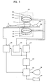
- Fig. 1 is a block diagram of an apparatus based on an embodiment of this invention.
- Fig. 2 is a diagram showing an example of pulse sequences implemented by the apparatus shown in Fig. 1.
- Fig. 3 is a diagram showing an example of pulse sequences implemented by the apparatus shown in Fig. 1.
- Fig. 4 is a schematic diagram showing the structure of the neighborhood of the sending coil section of the apparatus shown in Fig. 1.
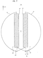
- Fig. 5 is a schematic diagram showing a pattern of current paths of the sending coil section shown in Fig. 4.
- Fig. 6 is a schematic diagram showing a pattern of current paths of the sending coil section shown in Fig. 4.
- Fig. 7 is a schematic diagram showing a pattern of current paths of the sending coil section shown in Fig. 4.
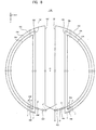
- Fig. 8 is a schematic diagram showing a pattern of current paths of the sending coil section shown in Fig. 4.
- Fig. 9 is a circuit diagram of the portion of disable circuits of the sending coil section shown in Fig. 8.
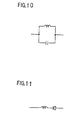
- Fig. 10 is a circuit diagram of an RF choke circuit.
- Fig. 11 is a circuit diagram of an RF choke circuit.
- Fig. 12 is a circuit diagram of the portion of disable circuits of the sending coil sections shown in Fig. 5 through Fig. 7.
- Fig. 13 is a schematic diagram showing patterns of current paths of the sending coil section shown in Fig. 4.
- Fig. 14 is a schematic diagram showing patterns of current paths of the sending coil section shown in Fig. 4.
- Fig. 15 is a schematic diagram showing a pattern of current paths of the sending coil section shown in Fig. 4.
- Fig. 16 is a schematic diagram showing patterns of current paths of the sending coil section shown in Fig. 4.
- FIG. 1 shows by block diagram a magnetic resonance imaging apparatus, which is an example of embodiment of this invention.
- the arrangement of this apparatus exhibits an example of embodiment of the inventive apparatus.
- this apparatus includes a magnet system 100.
- the magnet system 100 includes a magnet section 102 for a main magnetic field, a gradient coil section 106 and a sending coil section 108. These main-field magnet section 102 and coil sections are each arranged in pairs to confront each other by being interposed by a space. These devices having a generally disc-like shape are disposed along a common center axis.
- the magnet system 100 has an internal space (bore) where a subject 300 placed on a cradle 500 is carried in and out by a carriage means (not shown).
- a receiving coil section 110 is put on the imaging portion of the subject 300.
- the main-field magnet section 102 forms a static magnetic field in the bore of the magnet system 100.
- the static magnetic field is oriented to be virtually orthogonal to the body axis of the subject 300. Namely, it is so-called a vertical magnetic field.
- the main-field magnet section 102 is made up of permanent magnets for example. It is obviously possible to use magnets of the superconduction type or ordinary conduction type, instead of the permanent magnets.
- the gradient coil section 106 produces a gradient magnetic field which causes the static magnetic field to have a gradient.
- the produced gradient magnetic field consists of a slice gradient magnetic field, a read-out gradient magnetic field and a phase encode gradient magnetic field.
- the gradient coil section 106 includes gradient coils of three systems (not shown) in correspondence to these three kinds of gradient magnetic field.
- the gradient coils of three systems generate three gradient magnetic fields for rendering gradients to the static magnetic field in three directions which are orthogonal to one another.
- one is of the static magnetic field (vertical direction), which is defined to be the z direction in general.
- Other one is the horizontal direction, which is defined to be the y direction in general.
- the remaining one is the direction perpendicular to the y direction, and it is defined to be the x direction in general.
- the x direction is perpendicular to the z direction on a vertical plane, and perpendicular to the y direction on a horizontal plane.
- the sending coil section 108 transmits an RF excitation signal for inducing a spin in the body of the subject 300 into the space of static magnetic field.
- the sending coil section 108 is an example of embodiment of the inventive RF coil.
- the sending coil section 108 will be explained in detail later.
- the gradient coil section 106 is connected with a gradient drive section 130.
- the gradient drive section 130 supplies a drive signal to the gradient coil section 106, which then generates a gradient magnetic field.
- the gradient drive section 130 has drive circuits of three systems (not shown) in correspondence to the gradient coils of three systems of the gradient coil section 106.
- the sending coil section 108 is connected with an RF drive section 140.
- the RF drive section 140 supplies a drive signal to the sending coil section 108, which then transmits an RF excitation signal to induce a spin in the body of the subject 300.
- the RF drive section 140 also supplies a bias signal to disable circuits, which will be explained later, included in the sending coil section 108.
- the receiving coil section 110 receives a magnetic resonance signal produced by the induced spin.
- the receiving coil section 110 is connected with a data collecting section 150.
- the data collecting section 150 fetches signals received by the receiving coil section 110, thereby accumulating view data.
- the gradient drive section 130, RF drive section 140 and data collecting section 150 are connected with a control section 160.
- the control section 160 controls the gradient drive section 130, RF drive section 140 and data collecting section 150 to implement the imaging.
- the data collecting section 150 has its output connected to a data processing section 170.
- the data processing section 170 is a computer for example.
- the data processing section 170 has a memory (not shown).
- the memory stores programs and various data used by the data processing section 170. The function of this apparatus is accomplished by the execution of programs in the memory by the data processing section 170.
- the data processing section 170 store data, which has been fetched from the data collecting section 150, into the memory.
- a data space is formed in the memory.
- the data space is a 2-degree Fourier space.
- the data processing section 170 implements the inverse 2-degree Fourier transformation for the data of the 2-degree Fourier space thereby to produce (recompose) an image of the subject 300.
- the 2-degree Fourier space is also called a k-space.
- the data processing section 170 is connected to the control section 160.
- the data processing section 170 ranks above the control section 160, and administers it.
- the data processing section 170 is further connected with a display section 180 and operation section 190.
- the display section 180 is a graphic display unit or the like.
- the operation section 190 is a keyboard or the like equipped with a pointing device.
- the display section 180 displays a recomposed image and various information released by the data processing section 170.
- the operation section 190 is operated by the operator for entering various commands and information to the data processing section 170. The operator operates the apparatus in an interactive manner through the display section 180 and operation section 190.
- Fig. 2 shows an example of pulse sequences used for imaging by this apparatus. These pulse sequences are of the gradient echo (GRE) scheme.
- GRE gradient echo
- ⁇ ° pulse for RF excitation of the GRE scheme
- (2), (3), (4) and (5) are the sequences of slice gradient Gs, read-out gradient Gr and phase encode gradient Gp, and the gradient echo MR.
- the ⁇ ° pulse is represented by the center signal.
- the pulse sequences progress from left to right along the time axis t.
- the ⁇ ° pulse is used to implement the ⁇ ° excitation of spin as shown in the figure.
- the flip angle ⁇ ° is 90°or less.
- the slice gradient Gs is applied to implement the selective excitation for a certain slice.
- the ⁇ ° excitation is followed by phase encoding of the spin by the phase encode gradient Gp. Subsequently, the spin is dephased by the read-out gradient Gr, and next it is rephased to generate a gradient echo MR.
- the gradient echo MR has a peak of signal level on expiration of an echo time TE after the ⁇ ° excitation.
- the gradient echo MR is collected as view data by the data collecting section 150.
- pulse sequences are repeated 64-512 times at an interval of repetition time (TR).
- TR repetition time
- the phase encode gradient Gp is altered to implement different phase encoding.
- data of 64-512 views which fill the k-space is obtained.
- Fig. 3 shows another example of pulse sequences for magnetic resonance imaging. These pulse sequences are of the spin echo (SE) scheme.
- SE spin echo
- (1) are the sequences of 90°pulse and 180°pulse for RF excitation of the SE scheme
- (2), (3), (4) and (5) are the sequences of slice gradient Gs, read-out gradient Gr and phase encode gradient Gp, and the spin echo MR.
- the 90°pulse and 180°pulse are represented by the center signals.
- the pulse sequences progress from left to right along the time axis t.
- the 90°pulse is used to implement the 90°excitation of the spin as shown in the figure.
- selective excitation takes place for a certain slice, with the slice gradient Gs being applied thereto.
- the 180°excitation by the 180°pulse i.e., spin inversion, takes place.
- the same slice undergoes the selective inversion with the application of the slice gradient Gs.
- the read-out gradient Gr and phase encode gradient Gp are applied.
- the spin is dephased by the read-out gradient Gr.
- Phase encoding of the spin by the phase encode gradient Gp takes place.
- the spin is rephased by the read-out gradient Gr to generate a spin echo MR.
- the spin echo MR has a peak of signal level on expiration of TE after the 90°excitation.
- the spin echo MR is collected as view data by the data collecting section 150.
- the pulse sequences used for imaging are not confined to be of the GRE scheme or SE scheme, but can otherwise be of the fast spin echo (FSE) scheme, fast recovery fast spin echo (FSE) scheme, or echo planar imaging (EPI) scheme, for example.
- FSE fast spin echo
- FSE fast recovery fast spin echo
- EPI echo planar imaging
- the data processing section 170 implements the inverse 2-degree Fourier transformation for the view data of the k-space, thereby recomposing a tomographic image of the subject 300. Since the static magnetic field is rid of the adverse influence of the d.c. bias which disables the sending coil section 108, a high quality tomographic image is produced. The recomposed image is stored in the memory and also displayed on the display section 180.
- Fig. 4 shows schematically the cross-sectional structure of the portion of the magnet system 100 in the neighborhood of the sending coil section 108.
- letter o indicates the center of magnetic field, i.e., magnet center
- letters x, y and z indicate the three directions mentioned previously.
- a spheric volume SV having a center at the magnet center "o" and radius R defines an imaging region, and the magnet system 100 is designed so that the static magnetic field, gradient magnetic field and RF magnetic field are accurate as prescribed within the region SV.
- the main-field magnet section 102 in pairs has a pair of magnetic pole pieces 202 which confront each other.
- the pole pieces 202 are made of a magnetic material, such as soft iron, having a high permeability, and function to make a uniform flux distribution in the space of static magnetic field.
- the pole pieces 202 which have a generally disc-like shape, have their rim sections protruding in the direction normal to the disc surface (i.e., z direction) so as to face each other. Accordingly, each pole piece 202 has a base section and a protruding rim section. The rim sections function to regain the magnetic flux density that falls at the rim of the pole pieces 202.
- Each pole piece 202 has a recessed section formed inside the rim section, in which are fitted the gradient coil section 106 and sending coil section 108. Both coil sections having a generally disc-like shape are laid by being laminated on the surface of the pole piece 202 by a proper fixing means (not shown).
- Fig. 5 shows schematically a basic pattern of current paths of the RF coil which takes up the major portion of the sending coil section 108.
- the sending coil section 108 has, in its portion close to the center "o", two linear main current paths (main passes) 182 and 182' running in parallel to the y direction. These main passes 182 and 182' have a mirror-image relation with each other on the xy plane with respect to the y axis which passes through the center "o".
- the main passes 182 and 182' are an example of embodiment of the inventive main current paths.
- Return passes 192 and 192' lie round beside the main passes 182 and 182', respectively.
- the return passes 192 and 192' are an example of embodiment of the inventive roundabout current paths.
- the return pass 192 connects the main passes 182 and 182' in series so that they have a same current direction, while the return pass 192' connects the main passes 182' and 182 in series so that they have the same current direction.
- the return pass 192 is connected at its end joining to the main pass 182' with capacitors 402 and 404 in series, while the return pass 192' is connected at its end joining to the main pass 182 with capacitors 402' and 404' in series, so that these capacitors in unison with the main passes 182 and 182' and return passes 192 and 192' form an LC circuit.
- the LC circuit has its resonance frequency tuned to the magnetic resonance frequency.
- the capacitors 402 and 404 have their node grounded, and an RF drive signal which is produced against the ground is fed to the capacitor 402 from the RF drive section 140.
- one or more tuning capacitors may be connected in series at proper points on the main passes 182 and 182' and return passes 192 and 192' in addition to the capacitors 402 through 404'.
- the left terminal "a” of the capacitor 402 and the right terminal “a”' of the capacitor 402' on the drawing have an equal RF potential.
- the right terminal “b” of the capacitor 404 and the left terminal “b”' of the capacitor 404' have an equal RF potential.
- the points "a” and “a”' and the points "b” and “b”' have opposite polarities of potential.
- Fig. 8 shows, for example, a pattern of RF coil which enables a uniform distribution or arbitrary distribution of the RF magnetic field.
- the sending coil section 108 includes, in its portion close to the center "o", a number of linear main passes 182, 184, 186, 182', 184' and 186' which are parallel to the y direction.
- the main passes 182, 184 and 186 are progressively more distant in this order from the center "o", which affair is common to the main passes 182', 184' and 186'.
- the main passes 182, 184 and 186 are an example of embodiment of the inventive first current paths, while the main passes 182', 184' and 186' are an example of embodiment of the inventive second current paths.
- the main passes 182, 184 and 186 and the main passes 182', 184' and 186' have a mirror-image relation with each other on the xy plane with respect to the y axis which passes through the center "o".
- the number of main passes is arbitrary, instead of six in this example.
- Return passes 192, 194, 196, 192', 194' and 196' lie round beside the main passes.
- the return passes 192, 194, 196, 192', 194' and 196' are an example of embodiment of the inventive third current paths.
- the return pass 192 connects the main passes 182 and 184 in series so that they have a same current direction
- the return pass 194 connects the main passes 184 and 186 in series so that they have the same current direction
- the return pass 196 connects the main passes 186 and 182' in series so that they have the same current direction.
- the return pass 192' connects the main passes 182' and 184' in series to so that they have the same current direction
- the return pass 194' connects the main passes 184' and 186' in series so that they have the same current direction
- the return pass 196' connects the main passes 186' and 182 in series so that they have the same current direction.
- the return pass 196 is connected at its end joining to the main pass 182' with capacitors 402 and 404 in series, and the return pass 196' is connected at its end joining to the main pass 182 with capacitors 402' and 404' in series.
- the return pass 194 is connected at its end joining to the main pass 186 with a capacitor 406 in series, and the return pass 194' is connected at its end joining to the main pass 186' with a capacitor 406' in series.
- the return pass 192 is connected at its end joining to the main pass 184 with a capacitor 408 in series, and the return pass 192' is connected at its end joining to the main pass 184' with a capacitor 408' in series.
- More capacitors are inserted in series at proper points on the main passes 182 through 186' and return passes 192 through 196'. All of these capacitors in unison with the main passes 182 through 186' and return passes 192 through 196' form an LC circuit.
- the LC circuit has its resonance frequency tuned to the magnetic resonance frequency.
- the capacitors 402 and 404 have their node grounded, and an RF drive signal which is produced against the ground is fed to the capacitor 402 from the RF drive section 140.
- the main passes 182, 184, 186, 182', 184' and 186' are connected in series by the return passes 192, 194, 196, 192', 194' and 196' to have the same current direction. Consequently, all currents flowing through the main passes 182, 184, 186, 182', 184' and 186' have an equal value.
- the RF magnetic field has its distribution in the imaging space determined from the layout of the main passes 182 through 186' on the xy plane.
- the layout of the main passes 182 through 186' for establishing a uniform distribution or an intended distribution of the RF magnetic field can be determined by calculation.
- the left terminal "a” of the capacitor 402 and the right terminal “a”' of the capacitor 402' have an equal RF potential
- the right terminal "b” of the capacitor 404 and the left terminal “b”' of the capacitor 404' have an equal RF potential.
- the points "a” and “a”' and the points "b” and “b”' have opposite polarities of potential.
- the left terminal “c” of the capacitor 406 and the right terminal “c”' of the capacitor 406' have an equal RF potential
- the right terminal “d” of the capacitor 406 and the left terminal “d”' of the capacitor 406' have an equal RF potential.
- the points "c” and “c”' and the points "d” and “d”' have opposite polarities of potential.
- the left terminal “e” of the capacitor 408 and the right terminal “e”' of the capacitor 408' have an equal RF potential
- the right terminal “f” of the capacitor 408 and the left terminal “f” of the capacitor 408' have an equal RF potential.
- the points “e” and “e”' and the points "f” and “f”' have opposite polarities of potential.
- the points a, c, e, a', c' and e' have an equal RF potential
- the points b, d, f, b', d' and f' have an equal RF potential
- the points a, c, e, a', c' and e' and the points b, d, f, b', d' and f' have opposite polarities of potential.
- a d.c. bias feed path for the disable circuits is formed by means of RF choke circuits which interconnect the RF equipotential points (will be termed simply "equipotential points").
- Fig. 9 shows an example of the arrangement of the disable circuits.
- the figure is a schematic circuit diagram of the disable circuits fitted to the RF coil shown in Fig. 8.
- the disable circuits are part of the RF coil shown in Fig. 8.
- a capacitor 404 is connected in parallel with a serial circuit of an inductor 442 and a diode 444.
- a resistor 446 is connected in parallel to the diode 444.
- the resistor 446 is a high-resistance resistor.
- the circuit formed of the capacitor 404, inductor 442, diode 444 and resistor 446 constitutes a disable circuit.
- This disable circuit is an example of embodiment of the inventive disable circuit.
- an LC circuit is formed by the capacitor 404 and inductor 442.
- the LC circuit has its resonance frequency tuned to the frequency of the magnetic resonance signal, and it enters the high impedance state attributable to its parallel resonation, thereby performing the disable function.
- the diode With the diode being in the reverse bias state, the parallel connection of the capacitor 404 and inductor 442 dissolves, and the disable function is not brought into action.
- Similar disable circuits are formed of a capacitor 406 connected in parallel to a serial circuit of an inductor 462 and a diode 464, a capacitor 408 connected in parallel to a serial circuit of an inductor 482 and a diode 484, a capacitor 406' connected in parallel to a serial circuit of an inductor 462' and a diode 464', and a capacitor 408' connected in parallel to a serial circuit of an inductor 482' and a diode 484'.
- a high-resistance resistor is connected in parallel to each diode.
- the equipotential points a and a' are connected by an RF choke circuit 602.
- the equipotential points c and e are connected by an RF choke circuit 604.
- the equipotential points b and f are connected by an RF choke circuit 606.
- the equipotential points c' and e' are connected by an RF choke circuit 604'.
- the equipotential points b' and f' are connected by an RF choke circuit 606'.
- the equipotential points d and d' are connected by an RF choke circuit 608.
- the RF choke circuits 602, 604, 604', 606, 606' and 608 are an example of embodiment of the inventive RF choke circuits.
- the RF choke circuits 602, 604, 604', 606, 606' and 608 are each formed of an inductor which has large impedance values in the RF domain and small resistance values in the d.c. domain, for example.
- the RF choke circuit is not confined to this arrangement, but it may be, for example, an L-C parallel circuit tuned to the magnetic resonance signal as shown in Fig. 10, or an inductor having large impedance values in the RF domain connected in series with a diode as shown in Fig. 11. All of these RF choke circuits have large impedance values in the RF domain and small resistance values in the d.c. domain.
- This current path has no current flow due to the presence of the RF choke circuits 602, 604, 604', 606, 606' and 608 which connect the equipotential points of the path.
- All diodes on the current path lie in the same direction in terms of the polarity. Accordingly, supplying a d.c. forward bias current to the diodes through the current path forms L-C parallel circuits in the disable circuits, thereby effectuating their disable function. Conversely, applying a d.c. reverse bias voltage to the current path deactivates the disable circuits.
- Each diode has a parallel connection of a high-resistance resistor, which stabilizes the reverse bias voltage of the diode.
- disable circuits and associated bias signal feed circuit are formed in the same fashion as described above. These circuits are as shown in Fig. 12 for example.
- the RF coils shown in Fig. 5, Fig. 6 and Fig. 7 have a smaller number of disable circuits and RF choke circuits due to a smaller number of return passes as compared with that shown in Fig. 8.
- the bias signal for activating and deactivating the disable circuits can be applied to the terminals of the capacitor 402, i.e., the same points as to supply the RF drive signal. Accordingly, both the RF drive signal and bias signal can be supplied through common signal lines, instead of needing independent bias signal feed lines.
- the d.c. bias signal is conducted only through very small parts of the return pass and is not conducted through the main passes, and consequently a d.c. magnetic field created by the bias signal does not adversely affect the static magnetic field of the imaging space.
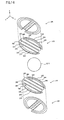
- a pair of sending coil sections 108 having the patterned coils, disable circuits and RF choke circuits are disposed to confront each other on both sides of the imaging space SV as shown in Fig. 13.
- the figure shows only the coil pattern expediently, which affair is common to the following figures.
- the sending coil sections 108 in pairs are supplied with drive signals of opposite polarities, and the sum of RF magnetic fields produced by the sending coil sections 108 is applied to the imaging space SV.
- the RF magnetic field induces a spin in the subject 300.
- one of the pair of sending coil sections 108 may be omitted.
- the main passes 182, 184 and 186 of one of the pair of sending coil sections 108 are an example of embodiment of the inventive first current paths
- the main passes 182', 184' and 186' are an example of embodiment of the inventive second current paths
- the return passes 192, 194, 196, 192', 194' and 196' are an example of embodiment of the inventive third current paths.
- the main passes 182, 184 and 186 of another of the pair of sending coil sections 108 are an example of embodiment of the inventive fourth current paths
- the main passes 182', 184' and 186' are an example of embodiment of the inventive fifth current paths
- the return passes 192, 194, 196, 192', 194' and 196' are an example of embodiment of the inventive sixth current paths.
- the sending coil section 108 may be accompanied face-to-face by another sending coil section 118 having its coil pattern rotated by 90°on the xy plane as shown in Fig. 14 for example, with both coil sections being insulates from each other obviously.
- Fig. 15 shows a coil pattern of the sending coil section 118. As shown in the figure, the sending coil section 118 is derived with 90°rotation from the coil pattern shown in Fig. 8.
- the sending coil section 118 includes, in its portion close to the center "o", linear main passes 282, 284, 286, 282', 284' and 286' which are parallel to the x direction.
- the main passes 282, 284 and 286 are progressively more distant in this order from the center "o", which affair is common to the main passes 282', 284' and 286'.
- the main passes 282, 284 and 286 are an example of embodiment of the inventive seventh current paths.
- the main passes 282', 284' and 286' are an example of embodiment of the inventive eighth current paths.
- Return passes 292, 294, 296, 292', 294' and 296' lie round beside the main passes.
- the return passes 292, 294, 296, 292', 294' and 296' are an example of embodiment of the inventive ninth current paths.
- the return pass 292 connects the main passes 282 and 284 in series so that they have a same current direction
- the return pass 294 connects the main passes 284 and 286 in series so that they have the same current direction
- the return pass 296 connects the main passes 286 and 282' in series so that they have the same current direction.
- the return pass 292' connects the main passes 282' and 284' in series to so that they have the same current direction
- the return pass 294' connects the main passes 284' and 286' in series so that they have the same current direction
- the return pass 296' connects the main passes 286' and 282 in series so that they have the same current direction.
- the return pass 296 is connected at its end joining to the main pass 282' with capacitors 502 and 504 in series, the return pass 296' is connected at its end joining to the main pass 282 with capacitors 502' and 504' in series.
- the return pass 294 is connected at its end joining to the main pass 286 with a capacitor 506 in series, the return pass 294' is connected at its end joining to the main pass 286' with a capacitor 506' in series.
- the return pass 292 is connected at its end joining to the main pass 284 with a capacitor 508 in series, the return pass 292' is connected at its end joining to the main pass 284' with a capacitor 508' in series.
- More capacitors are inserted in series at proper points on the main passes 282 through 286' and return passes 292 through 296'. All of these capacitors in unison with the main passes 282 through 286' and return passes 292 through 296' form an LC circuit.
- the LC circuit has its resonance frequency tuned to the magnetic resonance frequency.
- the capacitors 502 and 504 have their node grounded, and an RF drive signal which is produced against the ground is fed to the capacitor 502 from the RF drive section 140.
- the main passes 282, 284, 286, 282', 284' and 286' are connected in series by the return passes 292, 294, 296, 292', 294' and 296' to have the same current direction. Consequently, all currents flowing through the main passes 282, 284, 286, 282', 284' and 286' have an equal value.
- the RF magnetic field has its distribution in the imaging space determined from the layout of the main passes 282 through 286' on the xy plane.
- the layout of the main passes 282 through 286' for establishing a uniform distribution or an intended distribution of the RF magnetic field can be determined by calculation.
- the lower terminal "a” of the capacitor 502 and the upper terminal “a”' of the capacitor 502' have an equal RF potential
- the upper terminal "b” of the capacitor 504 and the lower terminal “b”' of the capacitor 504' have an equal RF potential.
- the points "a” and “a”' and the points "b” and “b”' have opposite polarities of potential.
- the lower terminal "c” of the capacitor 506 and the upper terminal “c”' of the capacitor 506' have an equal RF potential
- the upper terminal "d” of the capacitor 506 and the lower terminal “d”' of the capacitor 506' have an equal RF potential.
- the points "c” and “c”' and the points "d” and “d”' have opposite polarities of potential.
- the lower terminal “e” of the capacitor 508 and the upper terminal “e”' of the capacitor 508' have an equal RF potential
- the upper terminal “f” of the capacitor 508 and the lower terminal “f” of the capacitor 508' have an equal RF potential.
- the points “e” and “e”' and the points "f” and “f”' have opposite polarities of potential.
- the points a, c, e, a', c' and e' have an equal RF potential
- the points b, d, f, b', d' and f' have an equal RF potential
- the points a, c, e, a', c' and e' and the points b, d, f, b', d' and f' have opposite polarities of potential.
- disable circuits and associated bias signal feed circuit are formed in the same fashion as the RF coil 108.
- the bias signal feed circuits may be formed through the sending coil sections 108 and 118 in series.
- a pair of sending coil sections 118 having the patterned coils, disable circuits and RF choke circuits are disposed to confront each other together with the pair of sending coil sections 108 on both sides of the imaging space SV as shown in Fig. 16 for example.
- the sending coil sections 118 in pairs are supplied with drive signals of opposite polarities, and the sum of RF magnetic fields produced by the sending coil sections 118 is applied to the imaging space SV.
- the RF magnetic field induces a spin in the subject 300. In case a summed RF magnetic field is not necessary, one of the pair of sending coil sections 118 may be omitted.
- the main passes 282, 284 and 286 of one of the pair of sending coil sections 118 are an example of embodiment of the inventive seventh current paths
- the main passes 282', 284' and 286' are an example of embodiment of the inventive eighth current paths
- the return passes 292, 294, 296, 292', 294' and 296' are an example of embodiment of the inventive ninth current paths.
- the main passes 282, 284 and 286 of another of the pair of sending coil sections 118 are an example of embodiment of the inventive tenth current paths
- the main passes 282', 284' and 286' are an example of embodiment of the inventive eleventh current paths
- the return passes 292, 294, 296, 292', 294' and 296' are an example of embodiment of the inventive twelfth current paths.
- the sending coil sections 108 and 118 have their drive signals made opposite in phase by 90° thereby performing the so-called quadrature operation to produce an RF magnetic field which revolves on the xy plane within the imaging space SV.
- the RF magnetic field induces a spin in the subject 300.
Landscapes
- Physics & Mathematics (AREA)
- Condensed Matter Physics & Semiconductors (AREA)
- General Physics & Mathematics (AREA)
- Magnetic Resonance Imaging Apparatus (AREA)
Applications Claiming Priority (2)
| Application Number | Priority Date | Filing Date | Title |
|---|---|---|---|
| JP2000125490A JP3842520B2 (ja) | 2000-04-26 | 2000-04-26 | Rfコイルおよび磁気共鳴撮影装置 |
| JP2000125490 | 2000-04-26 |
Publications (3)
| Publication Number | Publication Date |
|---|---|
| EP1150134A2 true EP1150134A2 (de) | 2001-10-31 |
| EP1150134A3 EP1150134A3 (de) | 2001-12-19 |
| EP1150134B1 EP1150134B1 (de) | 2008-12-31 |
Family
ID=18635439
Family Applications (1)
| Application Number | Title | Priority Date | Filing Date |
|---|---|---|---|
| EP01303824A Expired - Lifetime EP1150134B1 (de) | 2000-04-26 | 2001-04-26 | RF-Spule und Gerät zur Bilderzeugung durch magnetische Resonanz |
Country Status (6)
| Country | Link |
|---|---|
| US (1) | US6580274B2 (de) |
| EP (1) | EP1150134B1 (de) |
| JP (1) | JP3842520B2 (de) |
| KR (1) | KR20010098858A (de) |
| CN (1) | CN1208023C (de) |
| DE (1) | DE60137163D1 (de) |
Families Citing this family (20)
| Publication number | Priority date | Publication date | Assignee | Title |
|---|---|---|---|---|
| JP3842520B2 (ja) * | 2000-04-26 | 2006-11-08 | ジーイー・メディカル・システムズ・グローバル・テクノロジー・カンパニー・エルエルシー | Rfコイルおよび磁気共鳴撮影装置 |
| US7010834B2 (en) * | 2002-09-10 | 2006-03-14 | Nokia Corporation | Hinge assembly, and associated method, providing multiple axes of rotation |
| US6798204B2 (en) * | 2002-10-09 | 2004-09-28 | Igc - Medical Advances, Inc. | Local RF MRI coil using metal foil construction on a double-sided substrate with holes that directly pass DC conductors |
| US6812703B2 (en) * | 2002-12-17 | 2004-11-02 | Varian, Inc. | Radio frequency NMR resonator with split axial shields |
| US6980000B2 (en) * | 2003-04-29 | 2005-12-27 | Varian, Inc. | Coils for high frequency MRI |
| JP4118833B2 (ja) * | 2004-04-16 | 2008-07-16 | ジーイー・メディカル・システムズ・グローバル・テクノロジー・カンパニー・エルエルシー | Mri用コイル |
| DE102006055136B4 (de) * | 2006-11-22 | 2010-05-06 | Siemens Ag | Hochfrequenzspulenanordnung und Magnetresonanzgerät |
| JP5229857B2 (ja) * | 2007-07-20 | 2013-07-03 | 株式会社日立メディコ | 磁気共鳴イメージング装置用高周波コイル、および、それを用いた磁気共鳴イメージング装置 |
| JP2009201886A (ja) * | 2008-02-29 | 2009-09-10 | Ge Medical Systems Global Technology Co Llc | コイル、mri装置、およびmriシステム |
| US8143891B2 (en) * | 2008-08-29 | 2012-03-27 | Siemens Aktiengesellschaft | System for image acquisition with fast magnetic resonance gradient echo sequences |
| US7855559B2 (en) * | 2008-09-30 | 2010-12-21 | General Electric Co. | Circuit and apparatus for decoupling RF surface coils |
| WO2011022356A1 (en) * | 2009-08-20 | 2011-02-24 | Med-El Elektromedizinische Geraete Gmbh | Mri-safe implant electronics |
| WO2011051872A2 (en) * | 2009-11-02 | 2011-05-05 | Koninklijke Philips Electronics N.V. | Radio frequency ablation catheter and magnetic resonance imaging system |
| JP5700129B2 (ja) * | 2011-08-09 | 2015-04-15 | 日立金属株式会社 | コイル装置及び磁気共鳴イメージング装置 |
| TWI541045B (zh) * | 2012-09-14 | 2016-07-11 | 國立成功大學 | 深度磁場產生裝置 |
| CN103837848B (zh) * | 2012-11-27 | 2017-05-17 | 朱宇东 | 用于磁共振系统中的射频天线装置及方法 |
| DE102014202301A1 (de) * | 2014-02-07 | 2015-08-13 | Siemens Aktiengesellschaft | Magnetresonanztomograph mit Patientenkommunikationseinrichtung und Verfahren zur akustischen Informationsübermittlung an einen Patienten in einem Magnetresonanztomographen |
| US10478087B2 (en) * | 2017-02-16 | 2019-11-19 | Aselsan Elektronik Sanayi Ve Ticaret A.S. | Open bore field free line magnetic particle imaging system |
| CN108627783B (zh) * | 2017-03-23 | 2022-01-14 | 通用电气公司 | 射频线圈阵列及磁共振成像发射阵列 |
| CN108931747B (zh) * | 2017-05-26 | 2024-02-06 | 苏州纽迈分析仪器股份有限公司 | 一种射频线圈 |
Family Cites Families (10)
| Publication number | Priority date | Publication date | Assignee | Title |
|---|---|---|---|---|
| JPH01293858A (ja) | 1988-05-20 | 1989-11-27 | Toshiba Corp | Rfコイル装置 |
| GB2221995B (en) * | 1988-08-19 | 1992-12-09 | Picker Int Ltd | Magnetic resonance methods and apparatus |
| US5075624A (en) * | 1990-05-29 | 1991-12-24 | North American Philips Corporation | Radio frequency quadrature coil construction for magnetic resonance imaging (mri) apparatus |
| DE4422781C1 (de) * | 1994-06-29 | 1996-02-01 | Siemens Ag | Aktiv geschirmte planare Gradientenspule für Polplattenmagnete |
| JP3502696B2 (ja) | 1995-06-05 | 2004-03-02 | ジーイー横河メディカルシステム株式会社 | Mri用rfコイル |
| JP3694558B2 (ja) | 1996-01-29 | 2005-09-14 | 株式会社日立メディコ | 高周波コイル及びそれを用いた磁気共鳴検査装置 |
| RU98106937A (ru) * | 1998-04-14 | 2000-02-10 | Пикер Нордстар ОЮ (FI) | Устройство для формирования изображения с помощью магнитного резонанса |
| US6249121B1 (en) * | 1999-05-17 | 2001-06-19 | General Electric Company | RF body coil |
| JP2001149331A (ja) * | 1999-11-19 | 2001-06-05 | Ge Medical Systems Global Technology Co Llc | 磁気共鳴信号受信装置および磁気共鳴撮像装置 |
| JP3842520B2 (ja) * | 2000-04-26 | 2006-11-08 | ジーイー・メディカル・システムズ・グローバル・テクノロジー・カンパニー・エルエルシー | Rfコイルおよび磁気共鳴撮影装置 |
-
2000
- 2000-04-26 JP JP2000125490A patent/JP3842520B2/ja not_active Expired - Fee Related
-
2001
- 2001-03-21 US US09/814,141 patent/US6580274B2/en not_active Expired - Fee Related
- 2001-04-25 KR KR1020010022272A patent/KR20010098858A/ko not_active Withdrawn
- 2001-04-26 DE DE60137163T patent/DE60137163D1/de not_active Expired - Fee Related
- 2001-04-26 CN CNB011174129A patent/CN1208023C/zh not_active Expired - Fee Related
- 2001-04-26 EP EP01303824A patent/EP1150134B1/de not_active Expired - Lifetime
Also Published As
| Publication number | Publication date |
|---|---|
| JP2001309901A (ja) | 2001-11-06 |
| DE60137163D1 (de) | 2009-02-12 |
| EP1150134A3 (de) | 2001-12-19 |
| JP3842520B2 (ja) | 2006-11-08 |
| CN1339703A (zh) | 2002-03-13 |
| US20010035754A1 (en) | 2001-11-01 |
| US6580274B2 (en) | 2003-06-17 |
| CN1208023C (zh) | 2005-06-29 |
| KR20010098858A (ko) | 2001-11-08 |
| EP1150134B1 (de) | 2008-12-31 |
Similar Documents
| Publication | Publication Date | Title |
|---|---|---|
| US6580274B2 (en) | RF coil and magnetic resonance imaging apparatus | |
| US6326789B1 (en) | Receive coil and magnetic resonance imaging method and apparatus | |
| DE68915536T2 (de) | Oberflächenspulen mit 90-grad-phasenverschiebung für die bildformung mittels magnetischer rezonanz. | |
| US5144243A (en) | RF coil system for use in magnetic resonance imaging apparatus | |
| US8415950B2 (en) | System and method for parallel transmission in MR imaging | |
| US20030088181A1 (en) | Method of localizing an object in an MR apparatus, a catheter and an MR apparatus for carrying out the method | |
| US6836117B2 (en) | Lower abdomen RF coil and magnetic resonance imaging apparatus | |
| WO1993003392A1 (en) | Magnetic resonance imaging techniques | |
| EP1109030A2 (de) | Vorrichtung zum Empfang magnetischer Resonanzsignale und Vorrichtung zur Bildgebung mit magnetischer Resonanz | |
| ATE161106T1 (de) | Positionierungs-system mit fernsteuerung zur bilderzeugung mittels magnetischer resonanz | |
| US7177671B2 (en) | RF coil, RF signal transmitter receiver, RF signal receiver, and magnetic resonance imaging system for the inferior abdomen | |
| Kuehne et al. | Pair of resonant fiducial markers for localization of endovascular catheters at all catheter orientations | |
| US6297636B1 (en) | RF coil, RF magnetic field generating apparatus and magnetic resonance imaging method and apparatus | |
| EP1122550A1 (de) | RF-Spulenarray mit reduzierter Kopplung zwischen den Spulen | |
| JPH0647017A (ja) | 動的に離調されるrf体積コイル | |
| JP2002159471A (ja) | 磁気共鳴画像化装置及びその方法 | |
| US6320383B1 (en) | RF coil, RF magnetic field generating apparatus and magnetic resonance imaging method and apparatus | |
| US6259251B1 (en) | RF coil and magnetic resonance imaging method and apparatus | |
| JP3705996B2 (ja) | 磁気共鳴撮影装置 | |
| KR100458780B1 (ko) | Rf 코일, 실드 및 자기 공명 촬상 장치 | |
| US5151655A (en) | Magnetic resonance imaging using a back-to-back pulse sequence | |
| US20170069453A1 (en) | Switch matrix assembly and magnetic resonance imaging apparatus using the same | |
| Celik et al. | Reverse polarized inductive coupling to transmit and receive radiofrequency coil arrays | |
| Ahmad et al. | Birdcage type NMR receiver coil sensor with integrated detuning circuit for 3T MRI system | |
| KR20010081364A (ko) | 수신 코일과 자기공진 촬상 방법 및 그 장치 |
Legal Events
| Date | Code | Title | Description |
|---|---|---|---|
| PUAI | Public reference made under article 153(3) epc to a published international application that has entered the european phase |
Free format text: ORIGINAL CODE: 0009012 |
|
| AK | Designated contracting states |
Kind code of ref document: A2 Designated state(s): AT BE CH CY DE DK ES FI FR GB GR IE IT LI LU MC NL PT SE TR Kind code of ref document: A2 Designated state(s): DE |
|
| AX | Request for extension of the european patent |
Free format text: AL;LT;LV;MK;RO;SI |
|
| PUAL | Search report despatched |
Free format text: ORIGINAL CODE: 0009013 |
|
| AK | Designated contracting states |
Kind code of ref document: A3 Designated state(s): AT BE CH CY DE DK ES FI FR GB GR IE IT LI LU MC NL PT SE TR |
|
| AX | Request for extension of the european patent |
Free format text: AL;LT;LV;MK;RO;SI |
|
| RAP1 | Party data changed (applicant data changed or rights of an application transferred) |
Owner name: GE MEDICAL SYSTEMS GLOBAL TECHNOLOGY COMPANY LLC |
|
| 17P | Request for examination filed |
Effective date: 20020619 |
|
| AKX | Designation fees paid |
Free format text: DE |
|
| 17Q | First examination report despatched |
Effective date: 20050915 |
|
| 17Q | First examination report despatched |
Effective date: 20050915 |
|
| GRAP | Despatch of communication of intention to grant a patent |
Free format text: ORIGINAL CODE: EPIDOSNIGR1 |
|
| GRAS | Grant fee paid |
Free format text: ORIGINAL CODE: EPIDOSNIGR3 |
|
| GRAA | (expected) grant |
Free format text: ORIGINAL CODE: 0009210 |
|
| AK | Designated contracting states |
Kind code of ref document: B1 Designated state(s): DE |
|
| REF | Corresponds to: |
Ref document number: 60137163 Country of ref document: DE Date of ref document: 20090212 Kind code of ref document: P |
|
| PGFP | Annual fee paid to national office [announced via postgrant information from national office to epo] |
Ref country code: DE Payment date: 20090429 Year of fee payment: 9 |
|
| PLBE | No opposition filed within time limit |
Free format text: ORIGINAL CODE: 0009261 |
|
| STAA | Information on the status of an ep patent application or granted ep patent |
Free format text: STATUS: NO OPPOSITION FILED WITHIN TIME LIMIT |
|
| 26N | No opposition filed |
Effective date: 20091001 |
|
| PG25 | Lapsed in a contracting state [announced via postgrant information from national office to epo] |
Ref country code: DE Free format text: LAPSE BECAUSE OF NON-PAYMENT OF DUE FEES Effective date: 20101103 |