EP1150363A2 - Actionneur piézoélectrique multicouche ayant un élément conducteur attaché à son électrode extérieure - Google Patents
Actionneur piézoélectrique multicouche ayant un élément conducteur attaché à son électrode extérieure Download PDFInfo
- Publication number
- EP1150363A2 EP1150363A2 EP01109675A EP01109675A EP1150363A2 EP 1150363 A2 EP1150363 A2 EP 1150363A2 EP 01109675 A EP01109675 A EP 01109675A EP 01109675 A EP01109675 A EP 01109675A EP 1150363 A2 EP1150363 A2 EP 1150363A2
- Authority
- EP
- European Patent Office
- Prior art keywords
- actuator device
- piezoelectric actuator
- internal electrodes
- multilayer structure
- multilayer
- Prior art date
- Legal status (The legal status is an assumption and is not a legal conclusion. Google has not performed a legal analysis and makes no representation as to the accuracy of the status listed.)
- Withdrawn
Links
- 239000002184 metal Substances 0.000 claims description 4
- 229910052751 metal Inorganic materials 0.000 claims description 4
- 239000011888 foil Substances 0.000 claims description 3
- 239000012212 insulator Substances 0.000 claims description 2
- 230000005855 radiation Effects 0.000 claims 1
- 230000015556 catabolic process Effects 0.000 description 4
- 239000000919 ceramic Substances 0.000 description 4
- 238000006731 degradation reaction Methods 0.000 description 4
- RYGMFSIKBFXOCR-UHFFFAOYSA-N Copper Chemical compound [Cu] RYGMFSIKBFXOCR-UHFFFAOYSA-N 0.000 description 3
- BQCADISMDOOEFD-UHFFFAOYSA-N Silver Chemical compound [Ag] BQCADISMDOOEFD-UHFFFAOYSA-N 0.000 description 3
- 238000005219 brazing Methods 0.000 description 3
- 239000011889 copper foil Substances 0.000 description 3
- 238000010304 firing Methods 0.000 description 3
- 229910052709 silver Inorganic materials 0.000 description 3
- 239000004332 silver Substances 0.000 description 3
- 230000008602 contraction Effects 0.000 description 2
- 230000008021 deposition Effects 0.000 description 2
- 230000000694 effects Effects 0.000 description 2
- PCHJSUWPFVWCPO-UHFFFAOYSA-N gold Chemical group [Au] PCHJSUWPFVWCPO-UHFFFAOYSA-N 0.000 description 2
- 239000010931 gold Substances 0.000 description 2
- 229910052737 gold Inorganic materials 0.000 description 2
- 238000002360 preparation method Methods 0.000 description 2
- 238000000576 coating method Methods 0.000 description 1
- 238000005516 engineering process Methods 0.000 description 1
- 239000011521 glass Substances 0.000 description 1
- WABPQHHGFIMREM-UHFFFAOYSA-N lead(0) Chemical compound [Pb] WABPQHHGFIMREM-UHFFFAOYSA-N 0.000 description 1
- 239000000463 material Substances 0.000 description 1
- 238000000034 method Methods 0.000 description 1
- 238000007650 screen-printing Methods 0.000 description 1
- 238000005476 soldering Methods 0.000 description 1
Images


Classifications
-
- H—ELECTRICITY
- H10—SEMICONDUCTOR DEVICES; ELECTRIC SOLID-STATE DEVICES NOT OTHERWISE PROVIDED FOR
- H10N—ELECTRIC SOLID-STATE DEVICES NOT OTHERWISE PROVIDED FOR
- H10N30/00—Piezoelectric or electrostrictive devices
- H10N30/80—Constructional details
- H10N30/87—Electrodes or interconnections, e.g. leads or terminals
- H10N30/872—Interconnections, e.g. connection electrodes of multilayer piezoelectric or electrostrictive devices
Definitions
- This invention relates to a multilayer piezoelectric actuator device in which a plurality of piezoelectric layers and a plurality of internal electrode layers are alternately stacked to form a multilayer structure so that each of the internal electrodes is placed between adjacent ones of the internal electrodes.
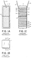
- the multilayer piezoelectric actuator device being illustrated comprises a multilayer structure 11 including a plurality of piezoelectric ceramics layers 11a and a plurality of internal electrodes 11b alternately laminated or stacked in a vertical stacking direction.
- the multilayer structure 11 has a side surface provided with a pair of external electrodes 12. Specifically, the external electrodes 12 are fixed to a pair of side surface portions opposite to each other in a direction perpendicular to the stacking direction, respectively.
- the external electrodes 12 are connected alternately to the internal electrodes 11b. Namely, adjacent ones of the internal electrodes 11b are connected to one and another of the external electrodes 12, respectively.
- Each of the external electrodes 12 may comprise a conductive member treated by firing of silver or deposition of gold.
- a pair of external lead wires 13 are connected to upper parts of the external electrodes 12, respectively.
- the external lead wires 13 are applied with a pulsed voltage.
- the pulsed voltage is applied, the multilayer piezoelectric actuator device repeats quick extension and contraction under the piezoelectric effect to provide a function as the actuator device.
- a multilayer piezoelectric actuator device which comprises a multilayer structure including a plurality of piezoelectric elements and a plurality of internal electrodes, the piezoelectric elements and the internal electrodes being stacked in a stacking direction so that each of the internal electrodes is placed between adjacent ones of the internal electrodes, a pair of external electrodes disposed on a side surface of the multilayer structure, the external electrodes being connected to adjacent ones of the internal electrodes, respectively, and a pair of conductive members connected to the external electrodes, respectively, each of the conductive member being spaced from and faced to the side surface of the multilayer structure.
- a multilayer piezoelectric actuator device which comprises a multilayer structure including a plurality of piezoelectric elements and a plurality of internal electrodes, the piezoelectric elements and the internal electrodes being stacked in a stacking direction so that each of the internal electrodes is placed between adjacent ones of the internal electrodes, a pair of external electrodes disposed on a side surface of the multilayer structure, the external electrodes being connected to adjacent ones of the internal electrodes, respectively, and a pair of conductive members connected to the external electrodes, respectively, each of the conductive member being spaced from and faced to the side surface of the multilayer structure, the side surface of the multilayer structure having a pair of side surface portions opposite to each other in a direction perpendicular to the stacking direction, the external electrodes being fixed to the side surface portions, respectively, the internal electrodes being alternately exposed on the side surface portions and connected to the external electrodes, respectively, each of the internal electrodes having an end face which is substantially flush with one of the side surface
- a multilayer piezoelectric actuator device which comprises a multilayer structure including a plurality of piezoelectric elements and a plurality of internal electrodes, the piezoelectric elements and the internal electrodes being stacked in a stacking direction so that each of the internal electrodes is placed between adjacent ones of the internal electrodes, a pair of external electrodes disposed on a side surface of the multilayer structure, the external electrodes being connected to adjacent ones of the internal electrodes, respectively, and a pair of conductive members connected to the external electrodes, respectively, each of the conductive member being spaced from and faced to the side surface of the multilayer structure, the side surface of the multilayer structure having a pair of side surface portions opposite to each other in a direction perpendicular to the stacking direction, the external electrodes being fixed to the side surface portions, respectively, the internal electrodes being alternately exposed on the side surface portions and connected to the external electrodes, respectively, each of the internal electrodes having an end face which is substantially flush with the side surface portions
- the multilayer piezoelectric actuator device being illustrated comprises a multilayer structure 1 including a plurality of piezoelectric ceramics layers 1a and a plurality of internal electrodes 1b alternately laminated or stacked in a vertical stacking direction.
- the multilayer structure 1 has a side surface provided with a pair of external electrodes 2.
- the external electrodes 2 are fixed to a pair of side surface portions opposite to each other in a direction perpendicular to the stacking direction, respectively.
- each of the piezoelectric layers 1a is made of a piezoelectric ceramics material.
- the internal electrodes 1 b are alternately exposed at one and another of the side surface portions of the multilayer structure 1. More particularly, odd-numbered ones of the internal electrodes 1b as counted from the lowermost one have one end faces substantially flush with and exposed on a left side surface of the multilayer structure 1 in Fig. 2C. On the other hand, even-numbered ones of the internal electrodes 1b have one end faces substantially flush with and exposed on a right side surface of the multilayer structure 1 in Fig. 2C. It is to be noted that the opposite end of each of the terminal electrodes 2 is retracted from the surface of the multilayer structure 1.
- Each of the external electrodes 2 is of a plate-like shape extending long in the above-mentioned stacking direction.
- the external electrodes 2 are connected alternately to the internal electrodes 1b on the side surface portions of the multilayer structure 1. Namely, adjacent ones of the internal electrodes 1b are connected to one and another of the external electrodes 2, respectively.
- Each of the external electrodes 2 may comprise a conductive member treated by firing of silver or deposition of gold.
- the external electrodes 2 extend in the stacking direction of the multilayer structure 1 and fixedly attached to the one side surface portion and the other side surface portion of the multilayer structure 1, respectively. Therefore, the external electrode 2 formed on the one side surface portion of the multilayer structure 1 is electrically connected to the odd-numbered ones of the internal electrodes 1b while the external electrode 2 formed on the other side surface portion of the multilayer structure 1 is electrically connected to the even-numbered ones of the internal electrodes 1b.
- a pair of external lead wires 5 are connected by soldering to upper parts of the external electrodes 2, respectively.
- the multilayer piezoelectric actuator device further comprises a pair of conductive members 3 coupled to the external electrodes 2, respectively.
- Each of the conductive members 3 is made of a metal foil such as a copper foil and extends in the stacking direction to be spaced from and faced to the side surface of the multilayer structure 3.
- Each of the conductive members 3 is slightly shorter than the external electrode 2 in the stacking direction.
- the conductive member 3 has one transversal end electrically and mechanically connected to the external electrode 2 by a brazing metal 4. On the other hand, the other transversal end of the conductive member 3 is not connected to anywhere at all and is a free end independent of the external electrode 2 and the multilayer structure 1.
- the piezoelectric ceramics actuator device illustrated in Figs. 2A through 2C at first, preparation is made of the multilayer structure 1 having a sectional size of 5mm square and a length of 60mm.
- the internal electrodes 1 b are alternately exposed on the one and the other side surface portions.
- the external electrodes 2 On the both side surface portions of the multilayer structure 1, the external electrodes 2 having a width of 2mm and a length of 55mm are formed by screen printing and firing a silver paste.
- preparation is made of the conductive member 3 of a copper foil having a width of 4mm, a length of 50mm, and a thickness of 50 ⁇ m.
- the one transversal end of the conductive member 3 is continuously attached by brazing to the external electrode 2. At this time, the other transversal end of the conductive member 3 is not connected to the external electrode 2. Finally, the external lead wire 5 is connected to one end of the external electrode 2.
- the multilayer piezoelectric actuator device illustrated in Figs. 2A through 2C and the multilayer piezoelectric actuator device illustrated in Figs. 1A through 1 C were driven 10 9 times by supplying a rectangular wave signal of 0-150V and 1 kHz.
- the external electrodes 12 were completely torn off by the crack 15 to cause current interruption. Therefore, the lower part of the multilayer structure 11 below the crack 15 was no longer operable.
- the multilayer piezoelectric actuator device illustrated in Figs. 2A through 2C brazed portions of the external electrodes 2 or the conductive members 3 were torn off by the crack 7.
- the multilayer piezoelectric actuator device is never degraded in function. This is because the conductive member 3 has an unconnected part not connected to the external electrode 2 by brazing and keeps electrical connection by the unconnected part that is prevented from being torn off.
- the multilayer piezoelectric actuator device illustrated in Figs. 2A through 2C is improved in durability and in reliability as compared with the multilayer piezoelectric actuator device illustrated in Figs. 1A through 1C. Furthermore, by connecting the conductive member 3 to the external electrode 2, the surface area of the actuator device is increased and the conductive member 3 serves as a heat sink to suppress the temperature elevation of the multilayer piezoelectric actuator device.
- each of all internal electrodes 1 b have opposite ends which are substantially flush with the opposite side surface portions of the multilayer structure 1, respectively.
- the internal electrodes 1 b are alternately covered with insulating glass coatings 8 and alternately uncovered or exposed. Therefore, like in the multilayer piezoelectric actuator device illustrated in Figs. 2A through 2C, the external electrodes 2 are alternately connected to the internal electrodes 1b so that every second ones and the remaining ones of the internal electrodes 1b are connected to one and the other of the external electrodes 2 on the opposite side surface portions, respectively.
- the conductive member 3 comprises a metal foil such as a copper foil.
- the conductive members 3 are formed on the side surface of the multilayer structure 1 to be spaced from and opposite to each other and extend long in the stacking direction.
- the multilayer piezoelectric actuator device illustrated in Figs. 3A through 3C also exhibits the effect equivalent to that achieved by the device illustrated in Figs. 2A through 2C.
- the multilayer piezoelectric actuator device As described above, in the multilayer piezoelectric actuator device according to this invention, degradation in function is suppressed even in occurrence of the crack in the multilayer structure and the external electrodes as a result of driving for a long period of time. In addition, it is possible to suppress the elevation of the device temperature.
Landscapes
- General Electrical Machinery Utilizing Piezoelectricity, Electrostriction Or Magnetostriction (AREA)
Applications Claiming Priority (2)
| Application Number | Priority Date | Filing Date | Title |
|---|---|---|---|
| JP2000118920 | 2000-04-20 | ||
| JP2000118920 | 2000-04-20 |
Publications (2)
| Publication Number | Publication Date |
|---|---|
| EP1150363A2 true EP1150363A2 (fr) | 2001-10-31 |
| EP1150363A3 EP1150363A3 (fr) | 2001-12-05 |
Family
ID=18629980
Family Applications (1)
| Application Number | Title | Priority Date | Filing Date |
|---|---|---|---|
| EP01109675A Withdrawn EP1150363A3 (fr) | 2000-04-20 | 2001-04-19 | Actionneur piézoélectrique multicouche ayant un élément conducteur attaché à son électrode extérieure |
Country Status (2)
| Country | Link |
|---|---|
| US (1) | US20010033125A1 (fr) |
| EP (1) | EP1150363A3 (fr) |
Cited By (3)
| Publication number | Priority date | Publication date | Assignee | Title |
|---|---|---|---|---|
| WO2005067071A1 (fr) * | 2004-01-08 | 2005-07-21 | Konkuk University | Structure d'actionneur piezo-electrique de ceramiques piezo-electriques possedant une couche d'activation ceramique laminee et son procede de fabrication |
| WO2006103192A1 (fr) * | 2005-03-29 | 2006-10-05 | Siemens Aktiengesellschaft | Unite d'activation piezo-electrique comprenant une capacite de conduction thermique ameliorer et injecteur de carburant |
| EP2587563A3 (fr) * | 2005-10-28 | 2014-09-17 | Kyocera Corporation | Élément piézoélectrique multicouche et dispositif d'injection l'utilisant |
Families Citing this family (6)
| Publication number | Priority date | Publication date | Assignee | Title |
|---|---|---|---|---|
| ATE538502T1 (de) * | 2005-02-15 | 2012-01-15 | Murata Manufacturing Co | Mehrschichtiges piezoelektrisches bauelement |
| JP2006303044A (ja) * | 2005-04-18 | 2006-11-02 | Denso Corp | 積層型圧電体素子 |
| JP4929875B2 (ja) * | 2006-06-30 | 2012-05-09 | 株式会社デンソー | 積層型圧電素子 |
| DE102008062021A1 (de) * | 2008-08-18 | 2010-03-04 | Epcos Ag | Piezoaktor in Vielschichtbauweise |
| DE102012109250B4 (de) * | 2012-09-28 | 2020-07-16 | Tdk Electronics Ag | Elektrisches Bauelement und Verfahren zur Herstellung einer Kontaktierung eines Elektrischen Bauelements |
| DE102015226143A1 (de) * | 2015-12-21 | 2017-06-22 | Robert Bosch Gmbh | Vielschichtaktor |
Citations (1)
| Publication number | Priority date | Publication date | Assignee | Title |
|---|---|---|---|---|
| JPH0476969A (ja) * | 1990-07-19 | 1992-03-11 | Nec Corp | 電歪効果素子 |
Family Cites Families (5)
| Publication number | Priority date | Publication date | Assignee | Title |
|---|---|---|---|---|
| EP0094078B1 (fr) * | 1982-05-11 | 1988-11-02 | Nec Corporation | Elément électrostrictif multicouche résistant à l'application répétée d'impulsions |
| DE19715487C2 (de) * | 1997-04-14 | 2002-06-13 | Siemens Ag | Piezoelektrischer Aktor mit einem Hohlprofil |
| DE19715488C1 (de) * | 1997-04-14 | 1998-06-25 | Siemens Ag | Piezoaktor mit neuer Kontaktierung und Herstellverfahren |
| DE19856185A1 (de) * | 1998-12-05 | 2000-06-15 | Bosch Gmbh Robert | Piezoelektrischer Antrieb |
| DE19857247C1 (de) * | 1998-12-11 | 2000-01-27 | Bosch Gmbh Robert | Piezoelektrischer Aktor |
-
2001
- 2001-04-18 US US09/836,998 patent/US20010033125A1/en not_active Abandoned
- 2001-04-19 EP EP01109675A patent/EP1150363A3/fr not_active Withdrawn
Patent Citations (1)
| Publication number | Priority date | Publication date | Assignee | Title |
|---|---|---|---|---|
| JPH0476969A (ja) * | 1990-07-19 | 1992-03-11 | Nec Corp | 電歪効果素子 |
Non-Patent Citations (1)
| Title |
|---|
| PATENT ABSTRACTS OF JAPAN vol. 016, no. 291 (E - 1224) 26 June 1992 (1992-06-26) * |
Cited By (4)
| Publication number | Priority date | Publication date | Assignee | Title |
|---|---|---|---|---|
| WO2005067071A1 (fr) * | 2004-01-08 | 2005-07-21 | Konkuk University | Structure d'actionneur piezo-electrique de ceramiques piezo-electriques possedant une couche d'activation ceramique laminee et son procede de fabrication |
| KR100587583B1 (ko) | 2004-01-08 | 2006-06-08 | 학교법인 건국대학교 | 적층형 세라믹 박판 작동층을 갖는 압전세라믹의 압전작동기 구조의 제조방법 |
| WO2006103192A1 (fr) * | 2005-03-29 | 2006-10-05 | Siemens Aktiengesellschaft | Unite d'activation piezo-electrique comprenant une capacite de conduction thermique ameliorer et injecteur de carburant |
| EP2587563A3 (fr) * | 2005-10-28 | 2014-09-17 | Kyocera Corporation | Élément piézoélectrique multicouche et dispositif d'injection l'utilisant |
Also Published As
| Publication number | Publication date |
|---|---|
| EP1150363A3 (fr) | 2001-12-05 |
| US20010033125A1 (en) | 2001-10-25 |
Similar Documents
| Publication | Publication Date | Title |
|---|---|---|
| US6522052B2 (en) | Multilayer-type piezoelectric actuator | |
| US6236146B1 (en) | Piezoelectric actuator with a new type of contacting and a method for the production thereof | |
| JP4154538B2 (ja) | 圧電アクチュエータ | |
| EP1950775B1 (fr) | Condensateur céramique monolithique | |
| US20020089266A1 (en) | External electrodes on piezoceramic multilayer actuators | |
| EP1150363A2 (fr) | Actionneur piézoélectrique multicouche ayant un élément conducteur attaché à son électrode extérieure | |
| JPH04159785A (ja) | 電歪効果素子 | |
| US6140749A (en) | Monolithic piezoelectric body and piezoelectric actuator | |
| WO2009125553A1 (fr) | Actionneur piézo-électrique laminé | |
| JP3307351B2 (ja) | 積層セラミックコンデンサ | |
| US20110181155A1 (en) | Piezoactuator with a Predetermined Breaking Layer | |
| JP2004534492A (ja) | ピエゾアクチュエータ | |
| JP2002009356A (ja) | 積層型圧電アクチュエータ素子 | |
| JP2000252537A (ja) | 積層型圧電セラミック | |
| JPH09270539A (ja) | 積層型圧電アクチュエータ | |
| US7679273B2 (en) | Strain tolerant metal electrode design | |
| JP2967562B2 (ja) | 圧電トランス及び圧電トランスの製造方法 | |
| JPH10270768A (ja) | 積層型圧電トランス | |
| JP3227896B2 (ja) | 積層型圧電体 | |
| JP3318686B2 (ja) | 積層型圧電アクチュエータ | |
| JP2505024Y2 (ja) | 積層セラミック電歪素子 | |
| JPH08162688A (ja) | 圧電トランスの電極構造 | |
| JPS60103685A (ja) | 積層型圧電体 | |
| JPH03225975A (ja) | 積層圧電アクチュエータ素子 | |
| JP3017784B2 (ja) | 積層型変位素子 |
Legal Events
| Date | Code | Title | Description |
|---|---|---|---|
| PUAI | Public reference made under article 153(3) epc to a published international application that has entered the european phase |
Free format text: ORIGINAL CODE: 0009012 |
|
| PUAL | Search report despatched |
Free format text: ORIGINAL CODE: 0009013 |
|
| AK | Designated contracting states |
Kind code of ref document: A2 Designated state(s): AT BE CH CY DE DK ES FI FR GB GR IE IT LI LU MC NL PT SE TR Kind code of ref document: A2 Designated state(s): DE FR GB |
|
| AX | Request for extension of the european patent |
Free format text: AL;LT;LV;MK;RO;SI |
|
| AK | Designated contracting states |
Kind code of ref document: A3 Designated state(s): AT BE CH CY DE DK ES FI FR GB GR IE IT LI LU MC NL PT SE TR |
|
| AX | Request for extension of the european patent |
Free format text: AL;LT;LV;MK;RO;SI |
|
| RIC1 | Information provided on ipc code assigned before grant |
Free format text: 7H 01L 41/083 A |
|
| 17P | Request for examination filed |
Effective date: 20020529 |
|
| AKX | Designation fees paid |
Free format text: DE FR GB |
|
| 17Q | First examination report despatched |
Effective date: 20020827 |
|
| RAP1 | Party data changed (applicant data changed or rights of an application transferred) |
Owner name: NEC TOKIN CERAMICS CORPORATION |
|
| STAA | Information on the status of an ep patent application or granted ep patent |
Free format text: STATUS: THE APPLICATION IS DEEMED TO BE WITHDRAWN |
|
| 18D | Application deemed to be withdrawn |
Effective date: 20041110 |