EP1150405A2 - Installation de commutation sous vide et son procédé de fabrication - Google Patents
Installation de commutation sous vide et son procédé de fabrication Download PDFInfo
- Publication number
- EP1150405A2 EP1150405A2 EP01107873A EP01107873A EP1150405A2 EP 1150405 A2 EP1150405 A2 EP 1150405A2 EP 01107873 A EP01107873 A EP 01107873A EP 01107873 A EP01107873 A EP 01107873A EP 1150405 A2 EP1150405 A2 EP 1150405A2
- Authority
- EP
- European Patent Office
- Prior art keywords
- conductive coating
- electric conductive
- molded insulator
- switch gear
- insulator
- Prior art date
- Legal status (The legal status is an assumption and is not a legal conclusion. Google has not performed a legal analysis and makes no representation as to the accuracy of the status listed.)
- Granted
Links
Images




Classifications
-
- H—ELECTRICITY
- H01—ELECTRIC ELEMENTS
- H01H—ELECTRIC SWITCHES; RELAYS; SELECTORS; EMERGENCY PROTECTIVE DEVICES
- H01H33/00—High-tension or heavy-current switches with arc-extinguishing or arc-preventing means
- H01H33/60—Switches wherein the means for extinguishing or preventing the arc do not include separate means for obtaining or increasing flow of arc-extinguishing fluid
- H01H33/66—Vacuum switches
-
- H—ELECTRICITY
- H01—ELECTRIC ELEMENTS
- H01H—ELECTRIC SWITCHES; RELAYS; SELECTORS; EMERGENCY PROTECTIVE DEVICES
- H01H33/00—High-tension or heavy-current switches with arc-extinguishing or arc-preventing means
- H01H33/60—Switches wherein the means for extinguishing or preventing the arc do not include separate means for obtaining or increasing flow of arc-extinguishing fluid
- H01H33/66—Vacuum switches
- H01H33/666—Operating arrangements
-
- H—ELECTRICITY
- H01—ELECTRIC ELEMENTS
- H01H—ELECTRIC SWITCHES; RELAYS; SELECTORS; EMERGENCY PROTECTIVE DEVICES
- H01H31/00—Air-break switches for high tension without arc-extinguishing or arc-preventing means
- H01H31/003—Earthing switches
-
- H—ELECTRICITY
- H01—ELECTRIC ELEMENTS
- H01H—ELECTRIC SWITCHES; RELAYS; SELECTORS; EMERGENCY PROTECTIVE DEVICES
- H01H33/00—High-tension or heavy-current switches with arc-extinguishing or arc-preventing means
- H01H33/02—Details
- H01H33/24—Means for preventing discharge to non-current-carrying parts, e.g. using corona ring
-
- H—ELECTRICITY
- H02—GENERATION; CONVERSION OR DISTRIBUTION OF ELECTRIC POWER
- H02B—BOARDS, SUBSTATIONS OR SWITCHING ARRANGEMENTS FOR THE SUPPLY OR DISTRIBUTION OF ELECTRIC POWER
- H02B13/00—Arrangement of switchgear in which switches are enclosed in, or structurally associated with, a casing, e.g. cubicle
- H02B13/02—Arrangement of switchgear in which switches are enclosed in, or structurally associated with, a casing, e.g. cubicle with metal casing
- H02B13/035—Gas-insulated switchgear
- H02B13/0354—Gas-insulated switchgear comprising a vacuum switch
-
- H—ELECTRICITY
- H01—ELECTRIC ELEMENTS
- H01H—ELECTRIC SWITCHES; RELAYS; SELECTORS; EMERGENCY PROTECTIVE DEVICES
- H01H33/00—High-tension or heavy-current switches with arc-extinguishing or arc-preventing means
- H01H33/60—Switches wherein the means for extinguishing or preventing the arc do not include separate means for obtaining or increasing flow of arc-extinguishing fluid
- H01H33/66—Vacuum switches
- H01H33/662—Housings or protective screens
- H01H33/66207—Specific housing details, e.g. sealing, soldering or brazing
- H01H2033/6623—Details relating to the encasing or the outside layers of the vacuum switch housings
-
- H—ELECTRICITY
- H01—ELECTRIC ELEMENTS
- H01H—ELECTRIC SWITCHES; RELAYS; SELECTORS; EMERGENCY PROTECTIVE DEVICES
- H01H33/00—High-tension or heavy-current switches with arc-extinguishing or arc-preventing means
- H01H33/60—Switches wherein the means for extinguishing or preventing the arc do not include separate means for obtaining or increasing flow of arc-extinguishing fluid
- H01H33/66—Vacuum switches
- H01H33/666—Operating arrangements
- H01H2033/6668—Operating arrangements with a plurality of interruptible circuit paths in single vacuum chamber
Definitions
- This invention relates to a vacuum insulated switch gear, particularly a vacuum insulated switch gear having an electric conductive coating formed by a thermal spraying process on an outer surface of a molded insulator covering a vacuum container, and a production method thereof.
- a ground layer is disposed on a surface of an insulator 13 of a solid insulated switch that molds a conductor 11 and a vacuum valve 12.
- reference numeral 14 denotes an electric conductive coating
- reference numeral denotes a control unit
- reference numeral 16 denotes an operation mechanism
- reference numeral 17 denotes an insertion device
- reference numeral 18 denotes a secondary switch plug
- reference numeral 19 denotes a line breaker portion
- reference numeral 20 denotes a cable head
- reference numeral 21 denotes a zero-phase current transformer
- reference numeral 22 denotes current transformer
- reference numeral 23 denotes an insulated bus.
- Japanese Patent Laid-Open Publication No. 61-109411 describes a method of forming a conductor layer on an insulator surface and a method of vacuum depositing or thermally spraying Zn or Pb on a surface of a shield of an insulator inside a gas container, as shown in Fig. 11.
- a conductor 25 is disposed inside a ground tank, that is, a container 24, storing an SF 6 gas as an insulating gas sealed therein.
- This conductor 25 is molded integrally with insulating spacers 26 and is supported by the insulating spacers 26 inside the tank.
- Reference numeral 27 denotes a conductor, too. The conductor 27 is electrically connected by a contact 28 with the conductor 25.
- a shield 29 for mitigating electrolysis encompasses the junction between both conductors 25 and 27 and is fixed to the conductor 25 by bolts 30.
- the bolts 30 fix mechanically the shield 29 to the conductor 25 and apply at the same time a pressure to the fixation surface between the shield 29 and the conductor 25 so that the shield 29 and the conductor 25 can be brought into close contact and can be electrically connected to each other.
- the shield 29 for mitigating electrolysis is a plastic component.
- a main body 29a of the plastic component 29 is covered with conduction means, that is, a conductor layer 29b, the plastic component 29 becomes electrically conductive.
- Japanese Patent Laid-Open Publication No. 2-303311 discloses application of a conductive paint, Zn thermal spraying, sputtering or metal plating to a surface of an electric field control ring made of an insulating material, as shown in Fig. 12.
- reference numeral 31 denotes a gas container
- reference numeral 32 denotes a conductor
- reference numeral 33 denotes an insulating spacer
- reference numeral 34 denotes a conductor
- reference numeral 35 denotes a contact
- reference numeral 36 denotes a field control ring.
- the field control ring 36 comprises a control ring main body 36a and a conductor film 36b.
- the conductive paint In the vacuum insulated switch gear according to the prior art having the construction described above, the conductive paint must be again coated in some cases from the aspect of durability. Since coating uses a solvent, a long time is necessary for drying the paint and the production cost increases. From the aspect of environmental pollution, too, the use of solvents must be avoided as much as possible.
- Vacuum deposition and sputtering involve the film formation inside a vacuum tank and are not suitable for mass-production and for production of large articles. In addition, because a film formation rate is low, a long time is necessary for processing and the production cost rises.
- Metal plating is of a wet system and needs a great deal of troubles in masking and drying in post-steps. In addition, this method cannot process large articles due to the sizes of a plating bath and a conveyor.
- Thermal spraying is a method of forming a coating by thermally spraying a molten metal in an open atmosphere to the surface of an insulator. Though relatively simple and economical, this method is not free from the problem that the use of Pb as a toxic material is preferably avoided from the aspect of environmental pollution.
- Thermal spraying of Zn is not only inferior in heat resistance but forms whiskers. Therefore, this method cannot be used for a portion on which an electric field concentrates.
- the electric field is likely to concentrate on an end face of the coating formed by thermal spraying because it is thin.
- the sprayed material dissociates from the surface of the insulator, or adheres to the insulator surface, thereby inviting the drop of dielectric strength.
- the present invention aims at providing a vacuum insulated switch gear having an electric conductive coating that can be economically produced and yet has high reliability.
- a vacuum insulated switch gear comprising a vacuum container for accommodating a switch portion, a molded insulator for surrounding the vacuum container and an electric conductive coating for covering the surface of the molded insulator, wherein the electric conductive coating is formed on an outer surface of the molded insulator by thermally spraying a melted material of at least one metal selected from the group consisting of Al, Cu, Ag, Ni, Cr, Fe, Ti and Zr in open air.
- a vacuum insulated switch gear comprising a vacuum container for accommodating a switch portion, a molded insulator for surrounding the vacuum container and an electric conductive coating for covering the surface of the molded insulator, wherein the electric conductive coating is formed on an outer surface of the molded insulator by thermally spraying a melted material of an oxide of at least one metal selected from the group consisting of Al, Cu, Ag, Ni, Cr, Fe, Ti and Zr in open air.
- a vacuum insulated switch gear comprising a vacuum container for accommodating a switch portion, a molded insulator for surrounding the vacuum container and an electric conductive coating, wherein the electric conductive coating is formed on an outer surface of the molded insulator by thermally spraying a melted material of a mixture of at least one metal selected from the group consisting of Al, Cu, Ag, Ni, Cr, Fe, Ti and Zr and an oxide of at least one metal selected from this group, to an outer surface of the molded insulator.
- the electric conductive coating formed by thermally spraying at least one metal selected from the group consisting of Al, Cu, Ag, Ni, Cr, Fe, Ti and Zr or an oxide of at least one metal selected from this group, or a mixture of this at least one metal and the oxide, to an outer surface of a molded insulator can be formed economically and moreover, with high reliability.
- the molded insulator includes a cylindrical portion that surrounds a vacuum container, end portions at both ends of the cylindrical portion, wherein a taper surface the diameter of which progressively increases towards the end of said the end portion is formed on a peripheral surface of at least one of the end portions of the cylindrical portion, and the end of the electric conductive coating is positioned on this taper surface.
- the molded insulator includes a cylindrical portion that surrouds a vacuum container, and end portions of the cylindrical portions, wherein an annular groove portion is formed on a peripheral surface of close to at least one of the end portions of the cylindrical portion, and the end of the electric conductive coating is positioned to this groove portion.
- the molded insulator includes a cylindrical portion that surrounds a vacuum container, and end portions of the cylindrical portion, wherein a slope surface is formed on the outer surface of at least one of the end portions of the cylindrical portion.
- the molded insulator includes a cylindrical portion that surrounds a vacuum container, and end portions of the cylindrical portion, wherein a step surface is formed on the outer surface of at least one of the end portions of the cylindrical portion.
- the molded insulator includes a cylindrical portion that surrounds a vacuum container and end portions of the cylindrical portion, wherein a taper surface is formed on the outer surface of at least one of the end portions of the cylindrical portion.
- the vacuum insulated switch gear according to the present invention further includes a sealant applied to an outer surface of the electric conductive coating described above, and this sealant prevents fall-off of a coating material from the surface of the electric conductive coating.
- a production method of a vacuum insulated switch gear according to the present invention comprising the steps of forming a molded insulator in such a manner as to surround a vacuum container accommodating therein a switch portion, and forming an electric conductive coating in such a manner as to cover a surface of the molded insulator, wherein the electric conductive coating is formed by thermally spraying at least one metal selected from the group consisting of Al, Cu, Ag, Ni, Cr, Fe, Ti and Zr to the surface of the molded insulator in open air.
- Another production method of a vacuum insulated switch gear comprising the steps of forming a molded insulator in such a manner as to surround a vacuum container accommodating therein a switch portion, and forming an electric conductive coating in such a manner as to cover a surface of the molded insulator, wherein the electric conductive coating is formed by thermally spraying an oxide of at least one metal selected from the group consisting of Al, Cu, Ag, Ni, Cr, Fe, Ti and Zr to a surface of the molded insulator in open air.
- Another production method of a vacuum insulated switch gear comprising the steps of forming a molded insulator in such a manner as to surround a vacuum container accommodating therein a switch portion, and forming an electric conductive coating in such a manner as to cover a surface of the molded insulator, wherein the electric conductive coating is formed by thermally spraying a mixture of at least one metal selected from the group consisting of Al, Cu, Ag, Ni, Cr, Fe, Ti and Zr and an oxide of at least one metal selected from this group to a surface of the molded insulator in open air.
- thermally sprays at least one metal selected from the group consisting of Al, Cu, Ag, Ni, Cr, Fe, Ti and Zr, or an oxide of at least one metal selected from this group, or a mixture of at least one metal selected from this group and an oxide of at least one metal selected from the group, to a surface of the molded insulator in open air can form economically an electric conductive coating having high reliability, and can economically produce a vacuum insulated switch gear having high reliability.
- Still another production method of a vacuum insulated switch gear according to the present invention applies air blow to an electric conductive coating after the electric conductive coating is formed by thermally spraying at least one metal described above to the surface of the molded insulator.
- Still another production method of a vacuum insulated switch gear according to the present invention applies shot blast to an electric conductive coating after the electric conductive coating is formed by thermally spraying at least one metal described above to the surface of the molded insulator.
- Still another production method of a vacuum insulated switch gear according to the present invention applies brushing to an electric conductive coating after the electric conductive coating is formed by thermally spraying at least one metal described above to the surface of the molded insulator.
- the coating material having low adhesive strength can be compulsively dropped from the surface of the electric conductive coating, and insulation performance can be improved.
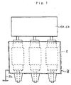
- Fig. 1 is a front view showing a vacuum insulated switch gear according to an embodiment 1 of the present invention and Fig. 2 is its sectional side view.
- reference numeral 1 denotes main circuit contact for breaking a circuit current.
- Reference numeral 2 denotes a ground contact for grounding a load circuit.
- Reference numerals 3 and 4 denote a conductor and a flexible conductor, respectively.
- Reference numeral 5 denotes a vacuum container for accommodating these circuit components.
- the vacuum container 5 is disposed for each of a three-phase electric circuit or in other words, three vacuum containers 5 in all are disposed in the three-phase electric circuit.
- Each vacuum container 5 accommodates the main circuit contact 1, the ground contact 2, the conductor 3 and the flexible conductor 4.
- Reference numerals 6a and 6b denote operation mechanisms for opening and closing the main circuit contact 1 and the ground contact 2, respectively.
- a common molded insulator 7 surround these three vacuum containers 5 constituting the three-phase electric circuit.
- the molded insulator 7 is injection-molded by charging an insulating resin such as an epoxy resin into a predetermined mold in such a manner as to collectively surround the three vacuum containers 5 that are aligned.
- An electric conductive coating 8 is formed on an outer surface of the molded insulator 7.
- the electric conductive coating 8 is grounded through a ground lead 8a to stabilize electric performance of the vacuum insulated switch gear.
- the electric conductive coating 8 is formed by thermally spraying a melted material of at least one metal selected from the group consisting of Al, Cu, Ag, Ni, Cr, Fe, Ti and Zr or a mixture of two or more of these metals to the outer surface of the molded insulator 7 in open air.
- An electric conductive coating 8 having electric conductivity can also be formed by thermally spraying a molten material of an oxide of at least one metal selected from the group described above, or a molten material of a mixture of at least one metal selected from the group described above and an oxide of at least one metal described above to the outer surface of the molded insulator 7 in open air.
- the electric conductive coating 8 formed by thermally spraying these metals or the metal oxide(s) in open air to the outer surface of the molded insulator 7 has higher durability than the conventional electric conductive coating.
- This electric conductive coating 8 does not need the use of a solvent for its formation unlike the conventional electric conductive coating and does not either need a long drying time. Therefore, it can lower the production cost.
- the metals of the group consisting of Al, Cu, Ag, Ni, Cr, Fe, Ti and Zr or their oxides do not form whiskers and do not either pollute the environment.
- the molten matter of the metals or the metal oxides or their mixture described above is thermally sprayed to the outer surface of the molded insulator 7 in open air to form the electric conductive coating 8. Therefore, the formation rate of the coating is higher than vacuum deposition and sputtering, or the electric conductive coating 8 can be formed within a shorter time, and the production cost can be lowered. In comparison with plating, the coating can be formed by a dry system, and troubles involved in the formation of the coating can be reduced.
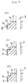
- Fig. 3 is a front view showing a vacuum insulated switch gear according to another embodiment, and Fig. 4 is its sectional side view.
- Reference numeral 1 denotes a main circuit contact for breaking a circuit current.
- Reference numeral 2 denotes a ground contact for grounding a load circuit.
- Reference numeral 3 denotes a conductor.
- Reference numeral 4 denotes a flexible conductor.
- Reference numeral 5 denotes a vacuum container that accommodates these circuit components.
- Thee vacuum containers 5 are disposed in alignment for a three-phase electric circuit. In this embodiment, these three vacuum containers 5 are individually surrounded with a molded insulator 7 of an epoxy resin, or the like.
- the electric conductive coating 8 described above is formed on the outer surface of each mold insulator 7 and is grounded.
- the electric conductive film 8 is formed by thermally spraying a molten material of at least one metal selected from the group consisting of Al, Cu, Ag, Ni, Cr, Fe, Ti and Zr or a molten material of an oxide of at least one metal selected from this group, or a molten matter of a mixture of at least one metal and an oxide of at least one metal selected from the group described above, to an outer surface of the molded insulator 7 in open air in the same way as in the embodiment shown in Figs. 1 and 2.
- An economical vacuum insulated switch gear having high reliability can be obtained in the same way.
- the present invention uses Al, Cu, Ag, Ni, Cr, Fe, Ti and Zr and their oxides and mixtures, that have higher melting points than the melting point of Zn, do not form whiskers, and are relatively economical and readily available, as the spray materials that are economical and have high heat resistance and high withstand voltage.
- the spray material may be those which consist of the materials described above as the principal component and contain other components to a certain extent. Such a material, too, exhibits similar effects.
- the vacuum container 5 may have any construction so long as it can accommodate the breaking portion, the disconnection portion and the ground switch portion. It is possible to employ the construction, for example, in which a space between adjacent arc grooves of a movable contact is connected to a movable rod, as described in Japanese Patent Laid-Open Publication No. 11-258185, or the construction in which a feeding structure to a movable electrode between a pair of opposed contacts is improved, as described in Japanese Patent Laid-Open Publication No. 11-41726.
- the present invention thermally sprays a metal such as Al, Cu, Ag, Ni, Cr, Fe, Ti or Zr, or its oxide or mixture to the surface of the molded insulator 7 of the vacuum insulated switch gear and forms the electric conductive coating. Therefore, the present invention can obtain the economical vacuum insulated switch gear having high reliability. Since the production method of the present invention can economically form the electric conductive coating with high reliability, the present invention is effective for improving reliability of the vacuum insulated switch gear and for reducing its cost of production.
- Embodiment 2 :
- Figs. 5 to 9 are sectional views each showing the surface shapes of the end portion of the sprayed coating 8 and the insulator 7.
- the drawings show the cases where the surface shape of the insulator 7 consists of a plurality of flat surfaces or curved surfaces.
- the structures shown in Figs. 5(a) and (b) correspond to the structures shown in Figs. 1 to 4, but the end portion of the sprayed coating 8 has a relatively high electric field.
- Fig. 5(c) shows the structure in which the sprayed coating 8 is positioned closer to the cylindrical portion 7b of the insulator 7 than its end face 7a.
- Figs. 6(a) and (b) show the structure in which a taper surface 7c which has an arc-shaped section and the diameter of which increases progressively towards the end face 7a is formed on an outer peripheral surface of the cylindrical portion 7b near at least one of the end faces 7a of the insulator 7 and the end portion of the electric conductive film 8 is positioned on this taper surface 7a.
- annular groove portion 7d having a semi-circular section is formed round the outer peripheral surface of the cylindrical portion 7b near at least one of the end faces 7a of the insulator 7 and the end portion of the electric conductive coating 8 is positioned to this groove portion 7d so as to prevent the occurrence of dielectric breakdown due to the concentration of the electric field. Furthermore, it is effective to form a slope surface 7e between at least one of the end faces 7a of the insulator 7 and the cylindrical portion 7b encompassing the vacuum container as shown in Figs. 7(a) to (c), or a section 7f between at least one of the end portions 7a of the insulator 7 and the cylindrical portion 7b encompassing the vacuum container, as shown in Figs. 8(a) to (c).
- Air blow can be conducted by spraying compressed air or a nitrogen gas of 2 to 7 atms. by using an air gun to the surface of the electric conductive coating 8 after spraying.
- the sprayed material having low adhesive strength on the outermost periphery of the electric conductive coating 8 can be compulsively dissociated, and reliability of insulating performance can be improved.
- Spraying of steel powder, ceramic powder, glass powder, plastic powder, dry ice, chaff, etc. may be sprayed by compressed air.
- the sprayed material having low adhesive strength on the outermost periphery of the electric conductive coating 8 can be compulsively dissociated or brought into close adhesion, and reliability of insulation performance can be improved.
- Brushing can be also made on the surface of the electric conductive coating 8 after its formation by spraying, by using a brush made of metals or fibers of nylon, or the like.
- the sprayed material having low adhesive strength on the outermost periphery of the electric conductive coating 8 can be compulsively dissociated and reliability of insulating performance can be improved.
- a silicone type or fluorine type sealant may be applied to the surface of the electric conductive coating 8 after its formation by spraying. In consequence, dissociation of the sprayed material having low adhesive strength on the outermost periphery of the electric conductive coating 8 can be prevented and reliability of insulation performance can be improved.
Landscapes
- Engineering & Computer Science (AREA)
- Power Engineering (AREA)
- Coating By Spraying Or Casting (AREA)
- Manufacture Of Switches (AREA)
- High-Tension Arc-Extinguishing Switches Without Spraying Means (AREA)
- Gas-Insulated Switchgears (AREA)
- Laminated Bodies (AREA)
Applications Claiming Priority (4)
| Application Number | Priority Date | Filing Date | Title |
|---|---|---|---|
| JP2000122164 | 2000-04-24 | ||
| JP2000122164 | 2000-04-24 | ||
| JP2000379609 | 2000-12-14 | ||
| JP2000379609A JP4537569B2 (ja) | 2000-04-24 | 2000-12-14 | 真空絶縁スイッチギヤ及びその製造方法 |
Publications (3)
| Publication Number | Publication Date |
|---|---|
| EP1150405A2 true EP1150405A2 (fr) | 2001-10-31 |
| EP1150405A3 EP1150405A3 (fr) | 2004-05-12 |
| EP1150405B1 EP1150405B1 (fr) | 2010-03-03 |
Family
ID=26590636
Family Applications (1)
| Application Number | Title | Priority Date | Filing Date |
|---|---|---|---|
| EP01107873A Expired - Lifetime EP1150405B1 (fr) | 2000-04-24 | 2001-04-10 | Installation de commutation sous vide et son procédé de fabrication |
Country Status (8)
| Country | Link |
|---|---|
| EP (1) | EP1150405B1 (fr) |
| JP (1) | JP4537569B2 (fr) |
| KR (1) | KR100417142B1 (fr) |
| CN (1) | CN1206684C (fr) |
| DE (1) | DE60141428D1 (fr) |
| HK (1) | HK1041555B (fr) |
| SG (1) | SG94793A1 (fr) |
| TW (1) | TW519786B (fr) |
Cited By (8)
| Publication number | Priority date | Publication date | Assignee | Title |
|---|---|---|---|---|
| WO2007022931A1 (fr) * | 2005-08-22 | 2007-03-01 | Abb Technology Ag | Procede de fabrication de poles d'interrupteur destines a des dispositifs de commutation basse, moyenne et haute frequence et pole d'interrupteur |
| EP1768149A1 (fr) * | 2005-09-27 | 2007-03-28 | Hitachi, Ltd. | Installation de commutation de multi-circuits |
| EP1693873A3 (fr) * | 2005-02-22 | 2007-10-17 | Hitachi, Ltd. | Installation de commutation à vide |
| EP2071687A1 (fr) * | 2007-12-10 | 2009-06-17 | ABB Technology AG | Ensemble de commutation moyenne tension ou haute tension |
| EP2026432A3 (fr) * | 2006-11-29 | 2009-06-17 | AREVA Energietechnik GmbH | Module de commutateur pour un dispositif de commutation électrique |
| US7679022B2 (en) | 2006-01-31 | 2010-03-16 | Hitachi, Ltd. | Vacuum insulated switchgear |
| CN105784569A (zh) * | 2016-04-12 | 2016-07-20 | 西安交通大学 | 一种研究gis内自由导电微粒运动的可视化实验平台 |
| CN108091519A (zh) * | 2018-01-25 | 2018-05-29 | 珠海康晋电气股份有限公司 | 一种可触摸的固封极柱装置 |
Families Citing this family (5)
| Publication number | Priority date | Publication date | Assignee | Title |
|---|---|---|---|---|
| JP4562584B2 (ja) * | 2005-05-12 | 2010-10-13 | 三菱電機株式会社 | 円筒形フィンガーコンタクトの銀めっき仕上げ方法 |
| CN101409175B (zh) * | 2008-01-14 | 2011-05-04 | 北京维益埃电气有限公司 | 组合式高压负荷开关及其高压开关设备 |
| CN102376419A (zh) * | 2010-08-12 | 2012-03-14 | 上海华明电力设备制造有限公司 | 鼓型无励磁分接开关绝缘筒的屏蔽方法 |
| CN103021726B (zh) * | 2012-12-27 | 2015-04-29 | 浙江雷安电气有限公司 | 固体绝缘筒 |
| DE102019211345A1 (de) | 2019-07-30 | 2021-02-04 | Siemens Energy Global GmbH & Co. KG | Unterbrechereinheit mit einer Vakuumröhre und einem Isoliergehäuse |
Family Cites Families (18)
| Publication number | Priority date | Publication date | Assignee | Title |
|---|---|---|---|---|
| US3956721A (en) * | 1975-04-16 | 1976-05-11 | Rte Corporation | Fault interrupter |
| US4150270A (en) * | 1976-02-23 | 1979-04-17 | Mcgraw-Edison Company | Encapsulated high voltage switching device |
| JPS5882512A (ja) * | 1981-11-11 | 1983-05-18 | Hitachi Ltd | モ−ルド変圧器 |
| JPS5923423A (ja) * | 1982-07-30 | 1984-02-06 | 株式会社明電舎 | 真空しや断器の真空度監視装置 |
| JPS58173146U (ja) * | 1983-03-23 | 1983-11-19 | 株式会社明電舎 | 完全固体絶縁型真空しや断器の真空度監視装置 |
| JPS61149338A (ja) * | 1984-12-25 | 1986-07-08 | Bridgestone Corp | ゴム又はプラスチツク成型品の製造方法 |
| JPH01278210A (ja) * | 1988-04-28 | 1989-11-08 | Toshiba Corp | ガス絶縁開閉装置 |
| JPH04132130A (ja) * | 1990-09-20 | 1992-05-06 | Meidensha Corp | 真空インタラプタの真空容器およびその製造方法 |
| JPH0622420A (ja) * | 1992-06-30 | 1994-01-28 | Toshiba Corp | スイッチギヤ |
| JP3302121B2 (ja) * | 1993-09-17 | 2002-07-15 | 株式会社東芝 | 真空バルブの製造方法 |
| JPH07147118A (ja) * | 1993-11-24 | 1995-06-06 | Toshiba Corp | 真空容器の製造方法 |
| JP3585517B2 (ja) * | 1994-02-15 | 2004-11-04 | 株式会社東芝 | ガス絶縁ブッシング |
| JPH08242513A (ja) * | 1995-03-01 | 1996-09-17 | Toshiba Corp | スイッチギヤ、電気機器 |
| JPH08306281A (ja) * | 1995-03-08 | 1996-11-22 | Fuji Electric Co Ltd | 真空遮断器用真空バルブ |
| JPH08250342A (ja) * | 1995-03-10 | 1996-09-27 | Matsushita Electric Ind Co Ltd | チップインダクタ |
| JP4276787B2 (ja) * | 1998-10-20 | 2009-06-10 | 株式会社日立製作所 | 真空スイッチギヤ |
| KR100370934B1 (ko) * | 1999-04-01 | 2003-02-05 | 미쓰비시덴키 가부시키가이샤 | 스위치 기어 및 전력 개폐기 |
| JP3577247B2 (ja) * | 1999-11-10 | 2004-10-13 | 三菱電機株式会社 | スイッチギア |
-
2000
- 2000-12-14 JP JP2000379609A patent/JP4537569B2/ja not_active Expired - Fee Related
-
2001
- 2001-03-15 TW TW090106047A patent/TW519786B/zh not_active IP Right Cessation
- 2001-03-22 SG SG200101877A patent/SG94793A1/en unknown
- 2001-04-10 DE DE60141428T patent/DE60141428D1/de not_active Expired - Lifetime
- 2001-04-10 EP EP01107873A patent/EP1150405B1/fr not_active Expired - Lifetime
- 2001-04-19 KR KR10-2001-0021139A patent/KR100417142B1/ko not_active Expired - Fee Related
- 2001-04-24 CN CNB011172053A patent/CN1206684C/zh not_active Expired - Fee Related
-
2002
- 2002-04-29 HK HK02103176.8A patent/HK1041555B/zh not_active IP Right Cessation
Cited By (12)
| Publication number | Priority date | Publication date | Assignee | Title |
|---|---|---|---|---|
| EP1693873A3 (fr) * | 2005-02-22 | 2007-10-17 | Hitachi, Ltd. | Installation de commutation à vide |
| US7902479B2 (en) | 2005-02-22 | 2011-03-08 | Hitachi, Ltd. | Vacuum switchgear |
| WO2007022931A1 (fr) * | 2005-08-22 | 2007-03-01 | Abb Technology Ag | Procede de fabrication de poles d'interrupteur destines a des dispositifs de commutation basse, moyenne et haute frequence et pole d'interrupteur |
| US7852180B2 (en) | 2005-08-22 | 2010-12-14 | Abb Technology Ag | Method for producing breaker pole parts for low-voltage, medium-voltage and high-voltage switchgear assemblies, and breaker pole part itself |
| EP1768149A1 (fr) * | 2005-09-27 | 2007-03-28 | Hitachi, Ltd. | Installation de commutation de multi-circuits |
| US7679022B2 (en) | 2006-01-31 | 2010-03-16 | Hitachi, Ltd. | Vacuum insulated switchgear |
| EP2026432A3 (fr) * | 2006-11-29 | 2009-06-17 | AREVA Energietechnik GmbH | Module de commutateur pour un dispositif de commutation électrique |
| EP2071687A1 (fr) * | 2007-12-10 | 2009-06-17 | ABB Technology AG | Ensemble de commutation moyenne tension ou haute tension |
| WO2009074256A1 (fr) * | 2007-12-10 | 2009-06-18 | Abb Technology Ag | Appareillage de commutation moyenne tension ou haute tension |
| CN105784569A (zh) * | 2016-04-12 | 2016-07-20 | 西安交通大学 | 一种研究gis内自由导电微粒运动的可视化实验平台 |
| CN105784569B (zh) * | 2016-04-12 | 2019-02-01 | 西安交通大学 | 一种研究gis内自由导电微粒运动的可视化实验平台 |
| CN108091519A (zh) * | 2018-01-25 | 2018-05-29 | 珠海康晋电气股份有限公司 | 一种可触摸的固封极柱装置 |
Also Published As
| Publication number | Publication date |
|---|---|
| JP4537569B2 (ja) | 2010-09-01 |
| EP1150405B1 (fr) | 2010-03-03 |
| EP1150405A3 (fr) | 2004-05-12 |
| HK1041555B (zh) | 2006-01-27 |
| SG94793A1 (en) | 2003-03-18 |
| TW519786B (en) | 2003-02-01 |
| HK1041555A1 (en) | 2002-07-12 |
| KR100417142B1 (ko) | 2004-02-05 |
| JP2002015645A (ja) | 2002-01-18 |
| CN1320941A (zh) | 2001-11-07 |
| CN1206684C (zh) | 2005-06-15 |
| DE60141428D1 (de) | 2010-04-15 |
| KR20010098747A (ko) | 2001-11-08 |
Similar Documents
| Publication | Publication Date | Title |
|---|---|---|
| EP1150405B1 (fr) | Installation de commutation sous vide et son procédé de fabrication | |
| US8178812B2 (en) | Insulation of a switchgear device of vacuum cartridge type by insert moulding | |
| EP2937958B1 (fr) | Équipement électrique isolé par gaz | |
| GB2173054A (en) | Subminiature fuses | |
| CN1065081C (zh) | 气体断路器 | |
| JP2005002474A (ja) | 中空体の内壁面を被覆する方法とそれによって被覆された中空体 | |
| EP2819258B1 (fr) | Appareillage de commutation isolé au gaz et barre omnibus isolée au gaz | |
| EP0344744A3 (fr) | Sectionneur pour appareil de communication à isolation gazeuse | |
| AU780289B2 (en) | Disconnector | |
| CN216981133U (zh) | 一种灭弧避雷器 | |
| CA1098157A (fr) | Blindages contre l'effet de couronne et methode de fabrication | |
| CA3179760C (fr) | Commutateur isole a l'air comprenant une longueur d'espace tres compacte | |
| CN218333588U (zh) | 一种上隔离固体绝缘开关结构 | |
| US6423903B1 (en) | Method and arrangement for minimizing electrical field stress in circuit interrupters and housings therefor | |
| JPS61288332A (ja) | 真空装置 | |
| JPH06119852A (ja) | ガス絶縁接地開閉装置 | |
| CN222546148U (zh) | 一种隔离触头 | |
| CN111371033B (zh) | 一种适用于高寒环境的环保型固体绝缘金属封闭开关设备 | |
| CN1111407A (zh) | 高压设备 | |
| JP2020092110A (ja) | 電界緩和シールド、ガス絶縁ブッシングおよび電界緩和シールドの製造方法 | |
| JP2000133094A (ja) | 投入抵抗付きガス遮断器 | |
| CA1114862A (fr) | Blindage semiconducteur anti-contrainte pour materiel a haute tension | |
| JPH02303311A (ja) | 注形絶縁物 | |
| CN1242588A (zh) | 配电系统中电开关设备的绝缘罩 | |
| JPH0237209Y2 (fr) |
Legal Events
| Date | Code | Title | Description |
|---|---|---|---|
| PUAI | Public reference made under article 153(3) epc to a published international application that has entered the european phase |
Free format text: ORIGINAL CODE: 0009012 |
|
| AK | Designated contracting states |
Kind code of ref document: A2 Designated state(s): AT BE CH CY DE DK ES FI FR GB GR IE IT LI LU MC NL PT SE TR |
|
| AX | Request for extension of the european patent |
Free format text: AL;LT;LV;MK;RO;SI |
|
| PUAL | Search report despatched |
Free format text: ORIGINAL CODE: 0009013 |
|
| AK | Designated contracting states |
Kind code of ref document: A3 Designated state(s): AT BE CH CY DE DK ES FI FR GB GR IE IT LI LU MC NL PT SE TR |
|
| AX | Request for extension of the european patent |
Extension state: AL LT LV MK RO SI |
|
| 17P | Request for examination filed |
Effective date: 20040705 |
|
| AKX | Designation fees paid |
Designated state(s): DE FR GB NL |
|
| RAP1 | Party data changed (applicant data changed or rights of an application transferred) |
Owner name: MITSUBISHI DENKI KABUSHIKI KAISHA |
|
| GRAP | Despatch of communication of intention to grant a patent |
Free format text: ORIGINAL CODE: EPIDOSNIGR1 |
|
| GRAS | Grant fee paid |
Free format text: ORIGINAL CODE: EPIDOSNIGR3 |
|
| GRAA | (expected) grant |
Free format text: ORIGINAL CODE: 0009210 |
|
| AK | Designated contracting states |
Kind code of ref document: B1 Designated state(s): DE FR GB NL |
|
| REG | Reference to a national code |
Ref country code: GB Ref legal event code: FG4D |
|
| REF | Corresponds to: |
Ref document number: 60141428 Country of ref document: DE Date of ref document: 20100415 Kind code of ref document: P |
|
| REG | Reference to a national code |
Ref country code: NL Ref legal event code: T3 |
|
| PLBE | No opposition filed within time limit |
Free format text: ORIGINAL CODE: 0009261 |
|
| STAA | Information on the status of an ep patent application or granted ep patent |
Free format text: STATUS: NO OPPOSITION FILED WITHIN TIME LIMIT |
|
| 26N | No opposition filed |
Effective date: 20101206 |
|
| REG | Reference to a national code |
Ref country code: FR Ref legal event code: PLFP Year of fee payment: 16 |
|
| PGFP | Annual fee paid to national office [announced via postgrant information from national office to epo] |
Ref country code: NL Payment date: 20160310 Year of fee payment: 16 |
|
| PGFP | Annual fee paid to national office [announced via postgrant information from national office to epo] |
Ref country code: FR Payment date: 20160309 Year of fee payment: 16 |
|
| PGFP | Annual fee paid to national office [announced via postgrant information from national office to epo] |
Ref country code: DE Payment date: 20160405 Year of fee payment: 16 Ref country code: GB Payment date: 20160406 Year of fee payment: 16 |
|
| REG | Reference to a national code |
Ref country code: DE Ref legal event code: R119 Ref document number: 60141428 Country of ref document: DE |
|
| REG | Reference to a national code |
Ref country code: NL Ref legal event code: MM Effective date: 20170501 |
|
| GBPC | Gb: european patent ceased through non-payment of renewal fee |
Effective date: 20170410 |
|
| REG | Reference to a national code |
Ref country code: FR Ref legal event code: ST Effective date: 20171229 |
|
| PG25 | Lapsed in a contracting state [announced via postgrant information from national office to epo] |
Ref country code: FR Free format text: LAPSE BECAUSE OF NON-PAYMENT OF DUE FEES Effective date: 20170502 Ref country code: DE Free format text: LAPSE BECAUSE OF NON-PAYMENT OF DUE FEES Effective date: 20171103 Ref country code: NL Free format text: LAPSE BECAUSE OF NON-PAYMENT OF DUE FEES Effective date: 20170501 |
|
| PG25 | Lapsed in a contracting state [announced via postgrant information from national office to epo] |
Ref country code: GB Free format text: LAPSE BECAUSE OF NON-PAYMENT OF DUE FEES Effective date: 20170410 |