EP1153675A2 - Strukturen aufweisender Materialstreifen - Google Patents
Strukturen aufweisender Materialstreifen Download PDFInfo
- Publication number
- EP1153675A2 EP1153675A2 EP01108886A EP01108886A EP1153675A2 EP 1153675 A2 EP1153675 A2 EP 1153675A2 EP 01108886 A EP01108886 A EP 01108886A EP 01108886 A EP01108886 A EP 01108886A EP 1153675 A2 EP1153675 A2 EP 1153675A2
- Authority
- EP
- European Patent Office
- Prior art keywords
- structures
- strip
- punched
- material strips
- edge
- Prior art date
- Legal status (The legal status is an assumption and is not a legal conclusion. Google has not performed a legal analysis and makes no representation as to the accuracy of the status listed.)
- Granted
Links
Images

Classifications
-
- B—PERFORMING OPERATIONS; TRANSPORTING
- B21—MECHANICAL METAL-WORKING WITHOUT ESSENTIALLY REMOVING MATERIAL; PUNCHING METAL
- B21D—WORKING OR PROCESSING OF SHEET METAL OR METAL TUBES, RODS OR PROFILES WITHOUT ESSENTIALLY REMOVING MATERIAL; PUNCHING METAL
- B21D43/00—Feeding, positioning or storing devices combined with, or arranged in, or specially adapted for use in connection with, apparatus for working or processing sheet metal, metal tubes or metal profiles; Associations therewith of cutting devices
- B21D43/20—Storage arrangements; Piling or unpiling
-
- B—PERFORMING OPERATIONS; TRANSPORTING
- B21—MECHANICAL METAL-WORKING WITHOUT ESSENTIALLY REMOVING MATERIAL; PUNCHING METAL
- B21D—WORKING OR PROCESSING OF SHEET METAL OR METAL TUBES, RODS OR PROFILES WITHOUT ESSENTIALLY REMOVING MATERIAL; PUNCHING METAL
- B21D28/00—Shaping by press-cutting; Perforating
- B21D28/02—Punching blanks or articles with or without obtaining scrap; Notching
- B21D28/10—Incompletely punching in such a manner that the parts are still coherent with the work
Definitions
- the invention relates to a material strip having structures with from the plane of the strip outstanding punching structures.
- the invention further relates to a strip composite as well as the use of the material strips.
- Such strips of material are relatively difficult to transport because, for example, intentionally Punch structures that protrude from the strip plane are not printed back into the plane during transport may be. This can be done relatively costly by intermediate layers, that serve as spacers.
- the invention has for its object to provide a simple and safe way stack the material strips characterized at the beginning without damage.
- stamping structures have the shape of a polygon, with an edge whose Length is less than two adjacent sides, with the strip of material connected to that the two adjacent sides at their ends facing away from the edge by two more Sides are connected to each other, the sides being symmetrical to a perpendicular the edge are arranged and each an angle ⁇ of about 20 ° to 80 ° to the perpendicular form and wherein punch openings formed by the punch structures in the material strip one cut free parallel to the sides adjacent to the edge Have slot.
- the punching structures serve as spacers and at the same time as fixation or centering several stripes against each other.
- the angle ⁇ is advantageously approximately 40 ° to 60 °.
- Another angle ⁇ between the perpendicular bisector on the edge and another Side is about 30 ° to 85 °, preferably 65 ° to 75 °. This allows relatively large distances between the strips can be achieved with precise positioning.
- the width of the cut slots has a ratio to the width the punching structure from about 1:10 to 1:40, the width of the cut slots is measured parallel to their longitudinal edges and the width of the punching structure is perpendicular to the perpendicular to the edge.
- the stamping structures an angle ⁇ of approximately 10 ° to 30 °, preferably approximately 20 °, to the vertical on the strip plane form. With the specified dimensions, optimal stacking behavior is guaranteed.
- the strip of material can be formed from metal.
- the punched structures are symmetrical to the central axis of the Are arranged material strip, and that in the material strip further structures, in particular punched structures are arranged.
- the strip composite formed from the material strips according to the invention is according to the Invention characterized in that the punched structures of a strip of material in punched openings of an adjacent strip of material, preferably that the others Sides of the stamping structures of a strip of material each on a boundary edge of the cut slots of the punching structures of an adjacent punching strip are supported are.
- the material strip having structures can be used for the production of in particular metallic lead frames can be used. Also a use for lead frames from other conductive materials is conceivable and provided according to the invention.
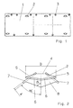
- a strip of material 1 made of copper is shown.
- punching structures 2 in evenly spaced along the two longitudinal edges of the material strip 1.
- Further punched structures 3 can be arranged on the material strip. This can serve as a means of positioning the material strips in further processing, however, they can also be functional in character from a strip of material have produced lead frame.
- FIG. 2 shows a punch structure 2 protruding from the strip plane.
- the punch structure 2 is connected at its edge 4 to the material strip 1.
- the remaining pages, that is to say the Edge 4 adjacent sides 5 and the other sides 6 connected to them are symmetrical arranged to a perpendicular to the edge 4.
- the ratio of the width A of the cut slots 7 to the width B of the stamping structure 2 is approximately 1:22
- the angle ⁇ between the adjacent ones Sides 5 and the perpendicular to the edge 4 about 50 °
- the angle ⁇ between another side 6 and the perpendicular bisector is about 70 °.
- a composite strip of two strips of material 1 is shown in a side view.
- the stamping structures 2 form an angle ⁇ of approximately 20 ° to the vertical on the Strip plane.
- the punch structures 2 of the lower material strip 1 engage in punch openings 8 of the upper strip of material 1.
- the other edges 6 of the stamping structures lie here 2 of the lower strip of material 1 on a boundary edge of the cut Slots 7 of the punch openings 8 of the adjacent material strip 1.
- vertical view (direction A) is this superimposed section shown in Fig. 4.
Landscapes
- Engineering & Computer Science (AREA)
- Mechanical Engineering (AREA)
- Punching Or Piercing (AREA)
- Laminated Bodies (AREA)
- Decoration Of Textiles (AREA)
- Polishing Bodies And Polishing Tools (AREA)
- Exhaust Gas After Treatment (AREA)
- Rod-Shaped Construction Members (AREA)
- Sliding-Contact Bearings (AREA)
Abstract
Description
- Fig. 1
- die schematische Darstellung eines Materialsteifens,
- Fig. 2
- eine Stanzstruktur des Materialstreifens,
- Fig. 3
- einen Streifenverbund in der Seitenansicht und
- Fig. 4
- eine ausschnittsweise Ansicht aus Richtung A gem. Fig. 3.
Claims (10)
- Strukturen aufweisender Materialstreifen mit aus seiner Streifenebene herausragenden Stanzstrukturen, dadurch gekennzeichnet, dass mindestens ein Teil der herausragenden Stanzstrukturen (2) die Form eines Vielecks aufweisen, das mit einer Kante (4), deren Länge kleiner ist als zwei angrenzende Seiten (5), mit dem Materialstreifen (1) verbunden ist, dass die beiden angrenzenden Seiten (5) an ihren der Kante (4) abgewandten Enden durch zwei weitere Seiten (6) miteinander verbunden sind, wobei die Seiten symmetrisch zu einer Mittelsenkrechten der Kante angeordnet sind und jeweils einen Winkel α von etwa 20° bis 80° zur Mittelsenkrechten bilden und wobei durch die Stanzstrukturen (2) in dem Materialstreifen (1) gebildete Stanzöffnungen (8) parallel zu den an die Kante (4) angrenzenden Seiten (5) je einen freigeschnittenen Schlitz (7) aufweisen.
- Strukturen aufweisender Materialstreifen nach Anspruch 1, dadurch gekennzeichnet, dass der Winkel α etwa 40° bis 60° beträgt.
- Strukturen aufweisender Materialstreifen nach einem der Ansprüche 1 oder 2, dadurch gekennzeichnet, dass die Breite der freigeschnittenen Schlitze (7) jeweils ein Verhältnis zur Breite der Stanzstruktur (2), parallel zur Kante (4) von etwa 1 : 10 bis 1 : 40 aufweist.
- Strukturen aufweisender Materialstreifen nach einem der Ansprüche 1 bis 3, dadurch gekennzeichnet, dass die Stanzstrukturen (2) einen Winkel γ von etwa 10° bis 30° vorzugsweise etwa 20°, zur Senkrechten auf der Streifenebene bilden.
- Strukturen aufweisender Materialstreifen nach einem der Ansprüche 1 bis 4, dadurch gekennzeichnet, dass der Materialstreifen (1) aus Metall gebildet ist.
- Strukturen aufweisender Materialstreifen nach einem der Ansprüche 1 bis 5, dadurch gekennzeichnet, dass die Stanzstrukturen (2) symmetrisch zur Mittelachse des Materialstreifens (1) angeordnet sind.
- Strukturen aufweisender Materialstreifen nach einem der Ansprüche 1 bis 6, dadurch gekennzeichnet, dass in dem Materialstreifen (1) weitere Strukturen (3), insbesondere gestanzte Strukturen, angeordnet sind.
- Streifenverbund aus mehreren flächig parallel zueinander angeordneten Strukturen aufweisenden Materialstreifen nach einem der Ansprüche 1 bis 7, dadurch gekennzeichnet, dass Stanzstrukturen (2) eines Materialstreifens (1) in Stanzöffnungen (8) eines benachbarten Materialstreifens (1) eingreifen.
- Streifenverbund Anspruch 8, dadurch gekennzeichnet, dass die weiteren Seiten (6) der Stanzstrukturen (2) eines Materialstreifens (1) jeweils auf einer Begrenzungskante der freigeschnittenen Schlitze (7) der Stanzöffnungen (8) eines benachbarten Materialstreifens (1) abgestützt sind.
- Verwendung der Strukturen aufweisenden Materialstreifen nach einem der Ansprüche 1 bis 7 zur Herstellung von metallischen Leiterrahmen.
Applications Claiming Priority (2)
| Application Number | Priority Date | Filing Date | Title |
|---|---|---|---|
| DE10022102A DE10022102C1 (de) | 2000-05-09 | 2000-05-09 | Strukturen aufweisender Materialstreifen |
| DE10022102 | 2000-05-09 |
Publications (3)
| Publication Number | Publication Date |
|---|---|
| EP1153675A2 true EP1153675A2 (de) | 2001-11-14 |
| EP1153675A3 EP1153675A3 (de) | 2004-10-27 |
| EP1153675B1 EP1153675B1 (de) | 2005-10-05 |
Family
ID=7641013
Family Applications (1)
| Application Number | Title | Priority Date | Filing Date |
|---|---|---|---|
| EP01108886A Expired - Lifetime EP1153675B1 (de) | 2000-05-09 | 2001-04-10 | Strukturen aufweisender Materialstreifen |
Country Status (6)
| Country | Link |
|---|---|
| EP (1) | EP1153675B1 (de) |
| CN (1) | CN1212223C (de) |
| AT (1) | ATE305831T1 (de) |
| DE (2) | DE10022102C1 (de) |
| ES (1) | ES2246269T3 (de) |
| MY (1) | MY130374A (de) |
Cited By (2)
| Publication number | Priority date | Publication date | Assignee | Title |
|---|---|---|---|---|
| WO2002007908A3 (en) * | 2000-07-11 | 2002-05-02 | Richard Smith | Method of enabling the spacing of metal units |
| CN102360927A (zh) * | 2011-09-07 | 2012-02-22 | 信源电子制品(昆山)有限公司 | 绕线镭射点焊机 |
Family Cites Families (3)
| Publication number | Priority date | Publication date | Assignee | Title |
|---|---|---|---|---|
| US4524601A (en) * | 1983-05-13 | 1985-06-25 | Bernardi Carl E | Automatic apparatus for downsetting lead frame strips |
| US4970579A (en) * | 1988-09-21 | 1990-11-13 | International Business Machines Corp. | Integrated circuit package with improved cooling means |
| DE19521022C2 (de) * | 1995-06-13 | 1997-04-10 | Heraeus Gmbh W C | Verfahren zur Herstellung eines Schichtverbundes |
-
2000
- 2000-05-09 DE DE10022102A patent/DE10022102C1/de not_active Expired - Fee Related
-
2001
- 2001-04-10 AT AT01108886T patent/ATE305831T1/de not_active IP Right Cessation
- 2001-04-10 DE DE50107591T patent/DE50107591D1/de not_active Expired - Fee Related
- 2001-04-10 ES ES01108886T patent/ES2246269T3/es not_active Expired - Lifetime
- 2001-04-10 EP EP01108886A patent/EP1153675B1/de not_active Expired - Lifetime
- 2001-05-04 MY MYPI20012101A patent/MY130374A/en unknown
- 2001-05-08 CN CN01116005.5A patent/CN1212223C/zh not_active Expired - Fee Related
Cited By (2)
| Publication number | Priority date | Publication date | Assignee | Title |
|---|---|---|---|---|
| WO2002007908A3 (en) * | 2000-07-11 | 2002-05-02 | Richard Smith | Method of enabling the spacing of metal units |
| CN102360927A (zh) * | 2011-09-07 | 2012-02-22 | 信源电子制品(昆山)有限公司 | 绕线镭射点焊机 |
Also Published As
| Publication number | Publication date |
|---|---|
| DE50107591D1 (de) | 2006-02-16 |
| ES2246269T3 (es) | 2006-02-16 |
| MY130374A (en) | 2007-06-29 |
| ATE305831T1 (de) | 2005-10-15 |
| DE10022102C1 (de) | 2001-10-25 |
| EP1153675A3 (de) | 2004-10-27 |
| EP1153675B1 (de) | 2005-10-05 |
| CN1212223C (zh) | 2005-07-27 |
| CN1322610A (zh) | 2001-11-21 |
Similar Documents
| Publication | Publication Date | Title |
|---|---|---|
| DE60016703T2 (de) | Verfahren zur Herstellung von Kühlkörper | |
| EP0072875B1 (de) | Einbauelement für eine Vorrichtung für Stoff-und direkten Wärmeaustausch und Mischen | |
| DE1400753B2 (de) | ||
| DE3016660C2 (de) | Sägeblatt | |
| DE10063248B4 (de) | Kommutatorausbildungsplatte, Verfahren zur Herstellung und Motor damit | |
| EP1153675B1 (de) | Strukturen aufweisender Materialstreifen | |
| EP1024247A1 (de) | Bohrwerkzeug | |
| AT328U1 (de) | Mechanische verbindung fuer leiterplatten zum aufbau raeumlicher gebilde aus flaechigem leiterplattenabfall | |
| DE8705002U1 (de) | Einbauhilfe zum Abschalen eines Betonbauteils in einem Anschlußbereich | |
| EP0092049B1 (de) | Lüftungsgitter für Gerätegehäuse | |
| DE202006020934U1 (de) | Förderkette | |
| DE3504726C1 (de) | Abschirmgehäuse für Hochfrequenz-Dünnschichtschaltungen | |
| CH620150A5 (en) | Letter perforator. | |
| DE102019114310B3 (de) | Flachsieb und Rundsieb | |
| DE2537241C3 (de) | Aus einem Gleitlagerwerkstoff ausgestanzte zur Herstellung einer Anlaufscheibenhälfte dienende Platine sowie Verfahren zu deren Herstellung | |
| DE10100020A1 (de) | Wischerarme sowie Verfahren zur Herstellung von Wischerarmen | |
| DE102018112037B3 (de) | Flachsieb | |
| DE2946196C2 (de) | Kontaktleiste | |
| DE112017007337T5 (de) | Pufferkappe für Aufzug | |
| DE3339905C1 (de) | Kesselflansch | |
| DE1400753C (de) | Verbindungselement | |
| DE102019114050A1 (de) | Stanzpaketieren von blechen | |
| EP3971924A1 (de) | Elektroisolierleistengitter | |
| DE2348686A1 (de) | Befestigungselement fuer kontaktbleche in mikrowellenbaugruppen | |
| AT37850B (de) | Verfahren zur Herstellung von Metallkeilen. |
Legal Events
| Date | Code | Title | Description |
|---|---|---|---|
| PUAI | Public reference made under article 153(3) epc to a published international application that has entered the european phase |
Free format text: ORIGINAL CODE: 0009012 |
|
| 17P | Request for examination filed |
Effective date: 20010417 |
|
| AK | Designated contracting states |
Kind code of ref document: A2 Designated state(s): AT BE CH CY DE DK ES FI FR GB GR IE IT LI LU MC NL PT SE TR |
|
| AX | Request for extension of the european patent |
Free format text: AL;LT;LV;MK;RO;SI |
|
| PUAL | Search report despatched |
Free format text: ORIGINAL CODE: 0009013 |
|
| AK | Designated contracting states |
Kind code of ref document: A3 Designated state(s): AT BE CH CY DE DK ES FI FR GB GR IE IT LI LU MC NL PT SE TR |
|
| AX | Request for extension of the european patent |
Extension state: AL LT LV MK RO SI |
|
| RAP1 | Party data changed (applicant data changed or rights of an application transferred) |
Owner name: W.C. HERAEUS GMBH |
|
| GRAP | Despatch of communication of intention to grant a patent |
Free format text: ORIGINAL CODE: EPIDOSNIGR1 |
|
| AKX | Designation fees paid |
Designated state(s): AT BE CH CY DE DK ES FI FR GB GR IE IT LI LU MC NL PT SE TR |
|
| GRAS | Grant fee paid |
Free format text: ORIGINAL CODE: EPIDOSNIGR3 |
|
| GRAA | (expected) grant |
Free format text: ORIGINAL CODE: 0009210 |
|
| AK | Designated contracting states |
Kind code of ref document: B1 Designated state(s): AT BE CH CY DE DK ES FI FR GB GR IE IT LI LU MC NL PT SE TR |
|
| PG25 | Lapsed in a contracting state [announced via postgrant information from national office to epo] |
Ref country code: GB Free format text: LAPSE BECAUSE OF FAILURE TO SUBMIT A TRANSLATION OF THE DESCRIPTION OR TO PAY THE FEE WITHIN THE PRESCRIBED TIME-LIMIT Effective date: 20051005 Ref country code: IE Free format text: LAPSE BECAUSE OF FAILURE TO SUBMIT A TRANSLATION OF THE DESCRIPTION OR TO PAY THE FEE WITHIN THE PRESCRIBED TIME-LIMIT Effective date: 20051005 |
|
| REG | Reference to a national code |
Ref country code: GB Ref legal event code: FG4D Free format text: NOT ENGLISH |
|
| REG | Reference to a national code |
Ref country code: CH Ref legal event code: EP Ref country code: CH Ref legal event code: NV Representative=s name: KIRKER & CIE SA |
|
| REG | Reference to a national code |
Ref country code: IE Ref legal event code: FG4D Free format text: LANGUAGE OF EP DOCUMENT: GERMAN |
|
| PG25 | Lapsed in a contracting state [announced via postgrant information from national office to epo] |
Ref country code: GR Free format text: LAPSE BECAUSE OF FAILURE TO SUBMIT A TRANSLATION OF THE DESCRIPTION OR TO PAY THE FEE WITHIN THE PRESCRIBED TIME-LIMIT Effective date: 20060105 Ref country code: DK Free format text: LAPSE BECAUSE OF FAILURE TO SUBMIT A TRANSLATION OF THE DESCRIPTION OR TO PAY THE FEE WITHIN THE PRESCRIBED TIME-LIMIT Effective date: 20060105 |
|
| REG | Reference to a national code |
Ref country code: SE Ref legal event code: TRGR |
|
| REF | Corresponds to: |
Ref document number: 50107591 Country of ref document: DE Date of ref document: 20060216 Kind code of ref document: P |
|
| REG | Reference to a national code |
Ref country code: ES Ref legal event code: FG2A Ref document number: 2246269 Country of ref document: ES Kind code of ref document: T3 |
|
| PG25 | Lapsed in a contracting state [announced via postgrant information from national office to epo] |
Ref country code: PT Free format text: LAPSE BECAUSE OF FAILURE TO SUBMIT A TRANSLATION OF THE DESCRIPTION OR TO PAY THE FEE WITHIN THE PRESCRIBED TIME-LIMIT Effective date: 20060306 |
|
| PG25 | Lapsed in a contracting state [announced via postgrant information from national office to epo] |
Ref country code: BE Free format text: LAPSE BECAUSE OF NON-PAYMENT OF DUE FEES Effective date: 20060430 Ref country code: MC Free format text: LAPSE BECAUSE OF NON-PAYMENT OF DUE FEES Effective date: 20060430 |
|
| GBV | Gb: ep patent (uk) treated as always having been void in accordance with gb section 77(7)/1977 [no translation filed] |
Effective date: 20051005 |
|
| REG | Reference to a national code |
Ref country code: IE Ref legal event code: FD4D |
|
| ET | Fr: translation filed | ||
| PLBE | No opposition filed within time limit |
Free format text: ORIGINAL CODE: 0009261 |
|
| STAA | Information on the status of an ep patent application or granted ep patent |
Free format text: STATUS: NO OPPOSITION FILED WITHIN TIME LIMIT |
|
| 26N | No opposition filed |
Effective date: 20060706 |
|
| BERE | Be: lapsed |
Owner name: W.C. HERAEUS G.M.B.H. Effective date: 20060430 |
|
| PG25 | Lapsed in a contracting state [announced via postgrant information from national office to epo] |
Ref country code: TR Free format text: LAPSE BECAUSE OF FAILURE TO SUBMIT A TRANSLATION OF THE DESCRIPTION OR TO PAY THE FEE WITHIN THE PRESCRIBED TIME-LIMIT Effective date: 20051005 Ref country code: LU Free format text: LAPSE BECAUSE OF NON-PAYMENT OF DUE FEES Effective date: 20060410 |
|
| PG25 | Lapsed in a contracting state [announced via postgrant information from national office to epo] |
Ref country code: CY Free format text: LAPSE BECAUSE OF FAILURE TO SUBMIT A TRANSLATION OF THE DESCRIPTION OR TO PAY THE FEE WITHIN THE PRESCRIBED TIME-LIMIT Effective date: 20051005 |
|
| PGFP | Annual fee paid to national office [announced via postgrant information from national office to epo] |
Ref country code: ES Payment date: 20090422 Year of fee payment: 9 |
|
| PGFP | Annual fee paid to national office [announced via postgrant information from national office to epo] |
Ref country code: AT Payment date: 20090416 Year of fee payment: 9 Ref country code: DE Payment date: 20090422 Year of fee payment: 9 Ref country code: FI Payment date: 20090417 Year of fee payment: 9 Ref country code: FR Payment date: 20090414 Year of fee payment: 9 Ref country code: IT Payment date: 20090423 Year of fee payment: 9 Ref country code: NL Payment date: 20090415 Year of fee payment: 9 Ref country code: SE Payment date: 20090416 Year of fee payment: 9 |
|
| PGFP | Annual fee paid to national office [announced via postgrant information from national office to epo] |
Ref country code: CH Payment date: 20090417 Year of fee payment: 9 |
|
| REG | Reference to a national code |
Ref country code: NL Ref legal event code: V1 Effective date: 20101101 |
|
| EUG | Se: european patent has lapsed | ||
| REG | Reference to a national code |
Ref country code: CH Ref legal event code: PL |
|
| REG | Reference to a national code |
Ref country code: FR Ref legal event code: ST Effective date: 20101230 |
|
| PG25 | Lapsed in a contracting state [announced via postgrant information from national office to epo] |
Ref country code: FI Free format text: LAPSE BECAUSE OF NON-PAYMENT OF DUE FEES Effective date: 20100410 Ref country code: NL Free format text: LAPSE BECAUSE OF NON-PAYMENT OF DUE FEES Effective date: 20101101 Ref country code: AT Free format text: LAPSE BECAUSE OF NON-PAYMENT OF DUE FEES Effective date: 20100410 |
|
| PG25 | Lapsed in a contracting state [announced via postgrant information from national office to epo] |
Ref country code: DE Free format text: LAPSE BECAUSE OF NON-PAYMENT OF DUE FEES Effective date: 20101103 Ref country code: CH Free format text: LAPSE BECAUSE OF NON-PAYMENT OF DUE FEES Effective date: 20100430 Ref country code: LI Free format text: LAPSE BECAUSE OF NON-PAYMENT OF DUE FEES Effective date: 20100430 |
|
| PG25 | Lapsed in a contracting state [announced via postgrant information from national office to epo] |
Ref country code: IT Free format text: LAPSE BECAUSE OF NON-PAYMENT OF DUE FEES Effective date: 20100410 |
|
| REG | Reference to a national code |
Ref country code: ES Ref legal event code: FD2A Effective date: 20110714 |
|
| PG25 | Lapsed in a contracting state [announced via postgrant information from national office to epo] |
Ref country code: ES Free format text: LAPSE BECAUSE OF NON-PAYMENT OF DUE FEES Effective date: 20110704 |
|
| PG25 | Lapsed in a contracting state [announced via postgrant information from national office to epo] |
Ref country code: ES Free format text: LAPSE BECAUSE OF NON-PAYMENT OF DUE FEES Effective date: 20100411 |
|
| PG25 | Lapsed in a contracting state [announced via postgrant information from national office to epo] |
Ref country code: FR Free format text: LAPSE BECAUSE OF NON-PAYMENT OF DUE FEES Effective date: 20100430 |
|
| PG25 | Lapsed in a contracting state [announced via postgrant information from national office to epo] |
Ref country code: SE Free format text: LAPSE BECAUSE OF NON-PAYMENT OF DUE FEES Effective date: 20100411 |