EP1156482A2 - Optisches Informationsaufzeichnungsgerät - Google Patents
Optisches Informationsaufzeichnungsgerät Download PDFInfo
- Publication number
- EP1156482A2 EP1156482A2 EP01111245A EP01111245A EP1156482A2 EP 1156482 A2 EP1156482 A2 EP 1156482A2 EP 01111245 A EP01111245 A EP 01111245A EP 01111245 A EP01111245 A EP 01111245A EP 1156482 A2 EP1156482 A2 EP 1156482A2
- Authority
- EP
- European Patent Office
- Prior art keywords
- pulse
- signal
- data
- recordation
- write
- Prior art date
- Legal status (The legal status is an assumption and is not a legal conclusion. Google has not performed a legal analysis and makes no representation as to the accuracy of the status listed.)
- Withdrawn
Links
Images


Classifications
-
- G—PHYSICS
- G11—INFORMATION STORAGE
- G11B—INFORMATION STORAGE BASED ON RELATIVE MOVEMENT BETWEEN RECORD CARRIER AND TRANSDUCER
- G11B7/00—Recording or reproducing by optical means, e.g. recording using a thermal beam of optical radiation by modifying optical properties or the physical structure, reproducing using an optical beam at lower power by sensing optical properties; Record carriers therefor
- G11B7/12—Heads, e.g. forming of the optical beam spot or modulation of the optical beam
- G11B7/125—Optical beam sources therefor, e.g. laser control circuitry specially adapted for optical storage devices; Modulators, e.g. means for controlling the size or intensity of optical spots or optical traces
- G11B7/126—Circuits, methods or arrangements for laser control or stabilisation
-
- G—PHYSICS
- G11—INFORMATION STORAGE
- G11B—INFORMATION STORAGE BASED ON RELATIVE MOVEMENT BETWEEN RECORD CARRIER AND TRANSDUCER
- G11B11/00—Recording on or reproducing from the same record carrier wherein for these two operations the methods are covered by different main groups of groups G11B3/00 - G11B7/00 or by different subgroups of group G11B9/00; Record carriers therefor
- G11B11/10—Recording on or reproducing from the same record carrier wherein for these two operations the methods are covered by different main groups of groups G11B3/00 - G11B7/00 or by different subgroups of group G11B9/00; Record carriers therefor using recording by magnetic means or other means for magnetisation or demagnetisation of a record carrier, e.g. light induced spin magnetisation; Demagnetisation by thermal or stress means in the presence or not of an orienting magnetic field
- G11B11/105—Recording on or reproducing from the same record carrier wherein for these two operations the methods are covered by different main groups of groups G11B3/00 - G11B7/00 or by different subgroups of group G11B9/00; Record carriers therefor using recording by magnetic means or other means for magnetisation or demagnetisation of a record carrier, e.g. light induced spin magnetisation; Demagnetisation by thermal or stress means in the presence or not of an orienting magnetic field using a beam of light or a magnetic field for recording by change of magnetisation and a beam of light for reproducing, i.e. magneto-optical, e.g. light-induced thermomagnetic recording, spin magnetisation recording, Kerr or Faraday effect reproducing
- G11B11/10502—Recording on or reproducing from the same record carrier wherein for these two operations the methods are covered by different main groups of groups G11B3/00 - G11B7/00 or by different subgroups of group G11B9/00; Record carriers therefor using recording by magnetic means or other means for magnetisation or demagnetisation of a record carrier, e.g. light induced spin magnetisation; Demagnetisation by thermal or stress means in the presence or not of an orienting magnetic field using a beam of light or a magnetic field for recording by change of magnetisation and a beam of light for reproducing, i.e. magneto-optical, e.g. light-induced thermomagnetic recording, spin magnetisation recording, Kerr or Faraday effect reproducing characterised by the transducing operation to be executed
- G11B11/1053—Recording on or reproducing from the same record carrier wherein for these two operations the methods are covered by different main groups of groups G11B3/00 - G11B7/00 or by different subgroups of group G11B9/00; Record carriers therefor using recording by magnetic means or other means for magnetisation or demagnetisation of a record carrier, e.g. light induced spin magnetisation; Demagnetisation by thermal or stress means in the presence or not of an orienting magnetic field using a beam of light or a magnetic field for recording by change of magnetisation and a beam of light for reproducing, i.e. magneto-optical, e.g. light-induced thermomagnetic recording, spin magnetisation recording, Kerr or Faraday effect reproducing characterised by the transducing operation to be executed to compensate for the magnetic domain drift or time shift
-
- G—PHYSICS
- G11—INFORMATION STORAGE
- G11B—INFORMATION STORAGE BASED ON RELATIVE MOVEMENT BETWEEN RECORD CARRIER AND TRANSDUCER
- G11B11/00—Recording on or reproducing from the same record carrier wherein for these two operations the methods are covered by different main groups of groups G11B3/00 - G11B7/00 or by different subgroups of group G11B9/00; Record carriers therefor
- G11B11/10—Recording on or reproducing from the same record carrier wherein for these two operations the methods are covered by different main groups of groups G11B3/00 - G11B7/00 or by different subgroups of group G11B9/00; Record carriers therefor using recording by magnetic means or other means for magnetisation or demagnetisation of a record carrier, e.g. light induced spin magnetisation; Demagnetisation by thermal or stress means in the presence or not of an orienting magnetic field
- G11B11/105—Recording on or reproducing from the same record carrier wherein for these two operations the methods are covered by different main groups of groups G11B3/00 - G11B7/00 or by different subgroups of group G11B9/00; Record carriers therefor using recording by magnetic means or other means for magnetisation or demagnetisation of a record carrier, e.g. light induced spin magnetisation; Demagnetisation by thermal or stress means in the presence or not of an orienting magnetic field using a beam of light or a magnetic field for recording by change of magnetisation and a beam of light for reproducing, i.e. magneto-optical, e.g. light-induced thermomagnetic recording, spin magnetisation recording, Kerr or Faraday effect reproducing
- G11B11/10595—Control of operating function
-
- G—PHYSICS
- G11—INFORMATION STORAGE
- G11B—INFORMATION STORAGE BASED ON RELATIVE MOVEMENT BETWEEN RECORD CARRIER AND TRANSDUCER
- G11B7/00—Recording or reproducing by optical means, e.g. recording using a thermal beam of optical radiation by modifying optical properties or the physical structure, reproducing using an optical beam at lower power by sensing optical properties; Record carriers therefor
- G11B7/004—Recording, reproducing or erasing methods; Read, write or erase circuits therefor
- G11B7/0045—Recording
Definitions
- the present invention relates to an optical information recording apparatus for recording a data pulse signal on an optical recording medium.
- An optical information recording apparatus for writing a data pulse signal consisting of consecutive pairs of mark (indicia) and space on an optical information recording medium such as CD (compact disk) and DVD (digital video disk or digital versatile disk) is known.
- a drive power (more specifically, drive current) for a semiconductor laser is on-off controlled in short periods in response to a write command signal to intermittently irradiate a laser beam at short periods, and this laser beam is used as a write beam to be irradiated onto the information recording medium via an optical system.
- control called write pulse strategy is performed to write and form pits having suitable recording characteristics on a recording layer.
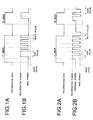
- Figures 1A and 1B of the accompanying drawings illustrate a write pulse strategy employed for DVD-R when information is written on a recording layer made from an organic pigment
- Figures 2A and 2B illustrate a write pulse strategy for DVD-RW when information is written on a recording film made from a phase change material.
- the DVD-R write pulse strategy provides a drive current to be fed to a semiconductor laser corresponding to recordation data in the form of pulse train and produces a write beam corresponding to recordation mark lengths of the recordation data according to a top pulse and subsequent multi-pulses, rather than simply conducting on-off control the drive current to be fed to the semiconductor laser in accordance with amplitude variations of the recordation data.
- the drive current for the semiconductor laser is controlled under such DVD-R write pulse strategy, thermal interference among the organic pigments of the recording layer is suppressed, and it is possible to prevent a rear end of a resulting pit from bulging and becoming like a tear drop due to heat accumulation. This also results in prevention of occurrence of jitter and crosstalk so that the DVD-R write pulse strategy is effective measures to improve recording characteristics.
- DVD-R write pulse strategy prevents the thermal interference from occurring and the pit rear end from becoming like a tear drop so that it can prevent the jitter and crosstalk.
- a drive current to the semiconductor laser corresponding to the recordation data is given in the form of pulse train, and a write beam corresponding to recordation mark lengths of the recordation data is generated in response to the top pulse, multi-pulses and cool pulse.
- the laser beam power varies between recordation power and bias power in accordance with the top and multi- pulses, and this variation causes the phase change material of the recording layer to be melt and cooled repeatedly such that amorphous is formed. Further, a laser beam of erasure power is irradiated during periods corresponding to the spaces of the recordation data so that the phase change material is crystallized. In this manner, the drive current of the semiconductor laser is controlled with the top, multi- and cool pulses to form recordation pits thereby improving recordation characteristics.
- the characteristics of recordation on the high density information recording medium are improved by controlling the recordation power of the write beam with the above described write pulse strategy or the like.
- the semiconductor laser element since the semiconductor laser element has an individual difference and environmental changes influence the semiconductor laser characteristics, it is sometimes difficult to set the recordation power of the write beam at a suitable power.
- waveforms time width and intensity
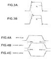
- the laser beam emitted from one semiconductor laser according to the common strategy pattern has such a waveform as shown in Figure 3A
- the laser beam emitted from the other semiconductor laser according to the commom strategy pattern has such a waveform as shown in Figure 3B.
- These waveforms are different from each other in rise time, fall time and irradiation period Ta and Tb so that the recordation characteristics on the information recording media are not the same as each other.
- a propagation delay period of the optical control circuit (a period until an in-phase output and inverted output are generated in response to a write pulse; see also Figures 4B and 4C) generally varies with the environmental temperature, and a rise time tPLH and a fall time tPHL of the propagation delay period also vary. If, for example, the rise time tPLH increases and the fall time tPHL decreases, the time for the drive current to drive the semiconductor laser becomes shorter and the irradiation time for the laser beam becomes shorter than an intended time period.
- the environmental temperature may influence not only the semiconductor laser element and optical control circuit, but also other circuits and electronic parts such as power source circuit used to drive the semiconductor laser element and optical control circuit. This results in nonuniform characteristics of the laser beams emitted from the semiconductor lasers and makes it difficult to have the same recordation characteristics on the information recording media.
- An object of the present invention is to provide an optical information recording apparatus that can eliminate the above described conventional problems.
- an optical information recording apparatus adapted to record a data pulse signal constituted by consecutive pairs of mark and space on an optical recording medium, comprising a drive pulse generator for generating a drive pulse in response to the data pulse signal, a light source element for generating a write beam in response to the drive pulse, and an optical system for irradiating the write beam onto the optical recording medium
- the drive pulse generator includes a write pulse generator for generating a write pulse signal based on the data pulse signal, a write beam intensity detector for detecting intensity of the write beam and generating a write beam intensity signal representing the detected intensity, an instruction pulse generator for comparing the write pulse signal with the write beam intensity signal and generating an instruction pulse which is obtained by regulating a pulse width of the write pulse in response to a comparison signal representing a result of comparison, and a drive unit for generating the drive pulse in response to the instruction pulse.
- a phase difference between a signal representing an actual chronological change of the intensity of the write beam irradiated onto the optical recording medium and the write signal based on the data pulse signal to be written on the recording media is detected, the pulse width of the drive pulse is regulated based on the detected phase difference, and the light source element such as a laser diode is driven with the regulated drive pulse.
- the drive pulse width is adjusted with the actual write beam variation such that the light source is optimally driven in such a manner that is free from influence by the changing environmental temperature and aging, thereby improving the recording characteristics to the information recording medium.
- FIG. 5 illustrated is a block diagram of an optical control circuit 100 for controlling a semiconductor laser incorporated in a pickup of a write device adapted to write information on DVD-R, which is an information recording medium.
- the optical control circuit 100 includes the pickup 4, a laser drive 3 and a recordation pulse generator 2.
- the write device includes a drive mechanism to rotate DVD-R at a predetermined linear velocity while keeping DVD-R at a predetermined clamp position during an information writing operation.
- the write device also includes a micro computer system having a micro processor (CPU) to perform centralized control over its operation.
- CPU micro processor
- the recordation pulse generator 2 generates a recordation pulse signal D2 based on a compensated recordation pulse data D1 supplied from a data generator for recordation pulse regulation 1, which is a regulation means, and feeds it to the laser drive 3.
- the compensated recordation pulse data D1 includes data specifying at least an amplitude and pulse width of the recordation pulse signal D2, and when this compensated recordation pulse data D1 is fed to the recordation pulse generator 2, a recordation pulse signal D2 having the specified amplitude and pulse width is produced and output.
- the recordation pulse generator 2 generates and outputs the recordation pulse signal D2 in accordance with the compensated recordation pulse data D1 which is digital data.
- the laser drive 3 has a variable current source including a current mirror circuit or the like, and controls an output current (drive current) D3 of the variable current source in response to variations of the recordation pulse signal amplitude.
- the laser drive feeds the drive current D3 to the pickup 4 in proportion to the amplitude of the recordation pulse signal D2.
- the pickup 4 includes an optical system (not shown), a semiconductor laser LD that accepts the drive current D3 from the laser drive 3, and a light receiving element or photo detector PD such as a photo diode located adjacent to the semiconductor laser LD.
- a laser beam radiated from the semiconductor laser LD is directed to a recording film of DVD-R through the optical system thereby to write information.
- the light receiving element PD detects part of the laser beam emitted from the semiconductor laser LD on the real time basis, and outputs the detection output as a monitoring signal D4. In other words, the light receiving element PD outputs the monitoring signal D4 that represents intensity of the laser beam irradiated on DVD-R.
- the optical control circuit 100 further includes a binary circuit 5 which serves as signal generating means, a strategy data extractor 6, the recordation pulse generator 7, a phase comparator 8, a low-pass filter 9, a gain regulator 10 and an A/D converter 11.
- the binary circuit 5 is a comparator that compares the monitoring signal D4 with a constant reference voltage Vref generated by a predetermined constant voltage source, and produces and outputs a binary signal D5. That is, the binary circuit 5 outputs a logic "H” as the binary signal D5 when the monitoring signal D4 is equal to or greater than the reference voltage Vref (D4 ⁇ Vref), and a logic "L” when the monitoring signal D4 is smaller than the reference voltage Vref (D4 ⁇ Vref). In other words, the binary circuit 5 generates and outputs the binary signal D5 that represents the chronological change of intensity of the laser beam actually irradiated to DVD-R from the semiconductor laser LD.
- the strategy data extractor 6 receives recordation data Din of the strategy pattern supplied from the computer system, extracts the top and multi-pulses included in the recordation data Din, as shown in Figure 7A, and produces and outputs digital data D6 representing generation timing, pulse widths and amplitudes of the top and multi-pulses.
- the computer system accepts digital data such as music data and computer programs, it converts the digital data to the recordation data Din of the strategy pattern as shown in Figure 7A based on a predetermined write pulse strategy, and feeds it to the strategy data extractor 6.
- the strategy data extractor 6 produces and outputs the digital data D6 that represents generation timing, pulse widths and amplitudes of the top and multi-pulses from the recordation data Din of the strategy pattern.
- the strategy data extractor 6 also transfers the recordation data Din of the strategy pattern given from the computer system directly to the recordation pulse regulation data generator 1.
- the recordation pulse generator 7 produces top and multi-pulses each being binary as shown in Figure 7A based on the digital data D6 from the strategy data extractor 6, and outputs a signal comprised of these top and multi-pulses as a recordation pulse signal D7.
- the recordation pulse generator 7 is a signal generation means for producing and outputting the ideal binary recordation pulse signal D7 based on the predetermined write pulse strategy.
- the phase comparator 8 compares the level of the binary signal D5 from the binary circuit 5 with that of the recordation pulse signal D7 from the recordation pulse generator 7 every time it receives the signals D5 and D7, detects a period during which both the signals D5 and D7 have the logic "H” and a period during which both the signals D5 and D7 have the logic "L”, so as to produce a detection signal D8.
- the phase comparator 8 is a decoder circuit, and as shown in Figure 6D, outputs a logic "H” as the detection signal D8 when the binary signal D5 is a logic “L” and the recordation pulse signal D7 is a logic “H”, a logic “L” when the binary signal D5 and recordation pulse signal D7 are both a logic “H”, a logic "-H” when the binary signal D5 is a logic "H” and the recordation pulse signal D7 is a logic “L”, and a logic "L” when the binary signal D5 and the recordation pulse signal D7 are both a logic "L”.
- the logic “H” is a predetermined voltage of positive polarity
- the logic “L” is a ground voltage
- the logic "-H” is a predetermined voltage of negative polarity having the same absolute value as the logic "H”.
- the period during which the detection signal D8 takes the logic “L” between the logic “H” and “-H” is detected as a period during which the binary signal D5 and the recordation pulse signal D7 both have the logic "H”. Further, the period during which the detection signal D8 takes the logic “L” between the logics “-H” and “H” is detected as a period during which the binary signal D5 and the recordation pulse signal D7 both have the logic "L”. Moreover, a phase difference between the binary signal D5 and recordation pulse signal D7 is detected from the period during which the detection signal D8 takes the logic "-H” or "H".
- the low-pass filter 9 smoothes the detection signal D8 and outputs a DC smoothed signal D9.
- the smoothed signal D9 is output in response to the changing detection signal D8, with the ground level (0V) being a reference.
- the gain regulator 10 is, for example, a variable gain voltage amplifier, and amplifies the smoothed signal D9 of trace level to a signal processable level and outputs an amplified smoothed signal D10.
- the A/D converter 11 performs an analog-digital conversion the smoothed signal D10 and outputs a smoothed data D11 representing a value proportional to the smoothed signal D10.
- the recordation pulse regulation data generator 1 Upon receiving the smoothed data D11, the recordation pulse regulation data generator 1 compensates the top and multi-pulses among the recordation data Din with the smoothed data D11, and feeds the compensated recordation pulse data D1 to the recordation pulse generator 2.
- the recordation pulse regulation data generator 1 generates the compensated recordation pulse data D1 in the following manner.
- the recordation data Din shown in Figure 7A is supplied to the recordation pulse regulation data generator 1 via the strategy data extractor 6, a period ⁇ a at the end of the top pulse and a period ⁇ b at the end of each multi-pulse in the recordation data Din are regulated (increased or decreased) respectively by an amount of time proportional to the value of the smoothed data D11 from the A/D converter 11.
- This increasing/decreasing regulation is conducted by a digital calculation, and the period-regulated data is supplied to the recordation pulse generator 2 as the compensated recordation pulse data D1 as shown in Figure 7B.
- the recordation pulse generator 2 outputs the recordation pulse signal D2 having the top and multi-pulses of which end periods ⁇ a and ⁇ b are adjusted based on the value of the smoothed data D11. Further, the laser drive 3 outputs the drive current D3 having a waveform analogous to the recordation pulse signal D2 and feeds it to the semiconductor laser LD.
- the light receiving element PD detects part of this laser beam and outputs the monitoring signal D4 ( Figure 6A) representing the change of the laser beam intensity.
- This monitoring signal D4 is compared with the reference voltage Vref in the binary circuit 5, and converted to the binary signal D5 ( Figure 6B) which is supplied to the phase comparator 8.
- the phase comparator 8 also receives the ideal recordation pulse signal D7 ( Figure 6C) from the recordation pulse generator 7.
- the phase comparator 8 compares the phase of the ideal recordation pulse signal D7 with that of the binary signal D5 obtained from the information recordation laser beam actually irradiated from the semiconductor laser LD to detect the phase difference, and outputs the detection signal D8 ( Figure 6D) representing the phase difference.
- the low-pass filter 9 smoothes this detection signal D8 to produce the smoothed signal D9 ( Figure 6E). After passing through the gain regulator 10, the smoothed signal D9 is converted to the smoothed data D11 by the A/D converter 11, and supplied to the recordation pulse regulation data generator 1.
- the recordation pulse regulation data generator 1 regulates the recordation data Din with the smoothed data D11, generates the compensated recordation pulse data D1 and supplies it to the recordation pulse generator 2, as described above.
- the compensated recordation pulse data D1 is supplied to the recordation pulse generator 2
- the recordation pulse signal D2 generated by the recordation pulse generator 2 using the compensated recordation pulse data D1 is supplied to the laser drive 3
- the laser drive 3 supplies the drive current D3 to the semiconductor laser LD.
- the drive current D3 that has the top and multi-pulses of which end periods ⁇ a and ⁇ b are adjusted via the feed-back operation based on the phase difference is supplied to the semiconductor laser LD.
- the periods ⁇ a and ⁇ b at the ends of the top and multi-pulses are adjusted by the above described feed-back control, and the light emission period of the semiconductor laser LD is appropriately controlled with the adjusted drive current D3, whereby the thermal interference in the organic pigments (recording layer) provided on the DVD-R is suppressed, the rear end of the formed pit is prevented from bulging and becoming like a tear drop, and other problems are also eliminated.
- Figure 8 is a block diagram showing a structure of an optical control circuit 200 according to this embodiment, and similar reference numerals are assigned to similar elements in Figures 5 and 8.
- the optical control circuit 200 includes a top pulse generator 7a and a multi-pulse generator 7b as signal generation means, and these pulse generators entail phase comparators 8a and 8b, low-pass filters 9a and 9b, gain regulators 10a and 10b, and A/D converters 11a and 11b respectively.
- the optical control circuit 200 includes a top pulse gate generator 12a, a multi-pulse gate generator 12b, and AND circuits 13a and 13b.
- the strategy data extractor 6 of this embodiment accepts the recordation data Din of the strategy pattern, extracts the top pulse and multi-pulses shown in Figure 7A, which are included in the recordation data Din, and generates and outputs digital data D6a representing the generation timing, pulse width and amplitude of the top pulse and digital data D6b representing the generation timing, pulse width and amplitude of the multi-pulses.
- the top pulse generator 7a only generates a top pulse as shown in Figure 7A based on the digital data D6a from the strategy data extractor 6, and outputs it as a recordation top pulse signal D7a. In other words, the top pulse generator 7a generates and outputs an ideal recordation top pulse signal D7a based on the predetermined write pulse strategy.
- the multi-pulse generator 7b only generates multi-pulses as shown in Figure 7A based on the digital data D6b from the strategy data extractor 6, and outputs them as a recordation multi-pulse signal D7b. In other words, the multi-pulse generator 7b generates and outputs an ideal recordation multi-pulse signal D7b based on the predetermined write pulse strategy.
- the top pulse gate generator 12a accepts a top pulse gate data DGa from the strategy data extractor 6, and generates and outputs a top pulse gate signal D12a in synchronization with the recordation top pulse signal D7a based on the data DGa.
- the strategy data extractor 6 outputs the digital data representing the top pulse D6a and the top pulse gate data DGa, and this top pulse gate data DGa is a data representing a generation period of the recordation top pulse signal D7a.
- the top pulse gate generator 12a generates and outputs a top pulse gate signal D12a that becomes a logic "H" in a period WT including the generation period of the recordation top pulse signal D7a based on the top pulse gate data DGa.
- the multi-pulse gate generator 12b receives a multi-pulse gate data DGb from the strategy data extractor 6, and generates and outputs a multi-pulse gate signal D12b in synchronization with the multi-pulse signal D7b based on the multi-pulse gate data DGb.
- the strategy data extractor 6 outputs the digital data D6b and the multi-pulse gate data DGb, and this multi-pulse gate data DGb is data representing a generation period of the recordation multi-pulse signal D7b.
- the multi-pulse gate generator 12b generates and outputs a multi- pulse gate signal D12b that becomes a logic "H" in a period WM including the generation period of the recordation multi-pulse signal D7b based on the multi-pulse gate data DGb.
- the AND circuit 13a obtains a logical product of the binary signal D5 from the binary circuit 5 and the top pulse gate signal D12a to produce and output the binary signal (referred to as "top detection signal” hereinafter) Da representing a top pulse component included in the binary signal D5.
- the AND circuit 13b obtains a logical product of the binary signal D5 from the binary circuit 5 and the multi-pulse gate signal D12b to produce and output the binary signal (referred to as "multi detection signal” hereinafter) Db representing a multi-pulse component included in the binary signal D5.
- a first route including the phase comparator 8a, low-pass filter 9a, gain regulator 10a and A/D converter 11a has fundamentally the same structure as a second route including the phase comparator 8b, low-pass filter 9b, gain regulator 10b and A/D converter 11b. Further, the first and second routes have fundamentally the same structure as a route including the phase comparator 8, low-pass filter 9, gain regulator 10 and A/D converter 11 shown in Figure 5.
- the phase comparator 8a detects a phase difference between the recordation top pulse signal D7a and top detection signal Da and outputs a detection signal D8a.
- the low-pass filter 9a smoothes the detection signal D8a and outputs a smoothed signal D9a.
- the gain regulator 10a amplifies the smoothed signal D9a to another smoothed signal D10a of signal processable level and outputs it.
- the A/D converter 11a converts the smoothed signal D10a to digital smoothed data D11a and supplies it to the recordation pulse regulation data generator 1.
- the phase comparator 8b detects a phase difference between the recordation multi-pulse signal D7b and multi detection signal Db and outputs a detection signal D8b.
- the low-pass filter 9b smoothes the detection signal D8b and outputs a smoothed signal D9b.
- the gain regulator 10b amplifies the smoothed signal D9b to another smoothed signal D10b of signal processable level and outputs it.
- the A/D converter 11b converts the smoothed signal D10b to digital smoothed data D11b and supplies it to the recordation pulse regulation data generator 1.
- Figures 9A to 10F are timing charts to describe a correction process made to the top pulse
- Figures 10A to 10F are timing charts to describe a correction process to the multi-pulse.
- the semiconductor laser LD irradiates a laser beam for information writing according to the drive current D3 from the laser drive 3
- the light receiving element PD detects part of this laser beam and outputs a monitoring signal D4 representing change of intensity of the laser beam as shown in Figure 9A.
- the monitoring signal D4 is compared with the reference voltage Vref in the binary circuit 5 and converted to the binary signal D5 as shown in Figures 9B and 10A before supplied to the AND circuits 13a and 13b.
- the A/D circuits 13a and 13b receive the top pulse gate signal D12a and multi-pulse gate signal D12b.
- the AND circuit 13a outputs the top detection signal Da representing the logical product of the top pulse gate signal D12a and the binary signal D5, as shown in Figure 9D, and feeds it to the phase comparator 8a.
- the AND circuit 13b outputs the multi detection signal Db representing the logical product of the multi-pulse gate signal D12b and the binary signal D5, as shown in Figure 10D, and feeds it to the phase comparator 8b.
- the phase comparator 8a detects a phase difference between the top detection signal Da and the recordation top pulse signal D7a and outputs a detection signal D8a as shown in Figure 9F.
- This detection signal D8a is smoothed to a smoothed signal D9a ( Figure 9G) and in turn to a smoothed signal D10a, which is then converted to a smoothed data D11a and fed to the recordation pulse regulation data generator 1.
- the phase comparator 8b detects a phase difference between the multi detection signal Db and the recordation multi-pulse signal D7b and outputs a detection signal D8b as shown in Figure 10E.
- This detection signal D8b is smoothed to a smoothed signal D9b ( Figure 10F) and in turn to a smoothed signal D10b, which is then converted to a smoothed data D11b and fed to the recordation pulse regulation data generator 1.
- the recordation pulse regulation data generator 1 regulates top pulse data included in the recordation data Din based on the smoothed data D11a and regulates multi-pulse data included in the recordation data Din based on the smoothed data D11b. Consequently, like the one illustrated in Figures 7A and 7B, a compensated recordation pulse data D1 of which top pulse end period ⁇ a and multi-pulse end period ⁇ b are regulated is generated and fed to the recordation pulse generator 2.
- the recordation pulse generator 2 As the recordation pulse generator 2 generates the recordation pulse signal D2 based on the compensated recordation pulse data D1 and supplies it to the laser drive 3, and the laser drive 3 supplies the drive current D3 to the semiconductor laser LD, the semiconductor laser LD irradiates the laser beam in accordance with the compensated recordation pulse data D1.
- this embodiment regulates the periods ⁇ a and ⁇ b at the top and multi-pulse ends by way of the above described feed back control and appropriately controls the irradiation periods of the semiconductor laser LD with the regulated drive current D3 so that the thermal interference among the organic pigments (recording layer) provided in DVD-R is suppressed and the rear end of the resulting pit does not bulge or become like a tear drop even if the characteristics of the semiconductor laser LD and those of the electronic parts and elements of the optical control circuit 200 vary with the environmental temperature and aging.
- FIG 11 illustrated is a block diagram showing a structure of an optical control circuit 300 according to this embodiment. Similar reference numerals are allotted to similar parts and elements in Figures 8 and 11.
- the optical control circuit 300 of this embodiment is adapted to control a write beam to be irradiated onto DVD-RW based on, for example, the write pulse strategy shown in Figures 2A and 2B.
- phase comparator 8c a phase comparator 8c, a low-pass filter 9c, a gain regulator 10c and an A/D converter 11c are connected to the cool pulse generator 7c.
- Still another difference is provision of a cool pulse gate generator 12c, two binary circuits 5ab and 5c, and an AND circuit 13c.
- the strategy data extractor 6 of the illustrated embodiment receives the recordation data Din of the strategy pattern, extracts the top and multi- pulses as shown in Figures 15A and 15B, which are included in the recordation data Din, and generates and outputs digital data D6a representing the generation timing, pulse width and amplitude of the top pulse, digital data D6b representing generation timing, pulse width and amplitude of the multi-pulse, and digital data D6c representing generation timing, pulse width and amplitude of the cool pulse.
- the cool pulse generator 7c generates only the cool pulse based on the digital data D6c from the strategy data extractor 6 and outputs it as a recordation cool pulse signal D7c.
- the top pulse generator 7a and multi-pulse generator 7b generate the top and multi-pulses based on the digital data D6a and D6b from the strategy data extractor 6 respectively, and output the resulting signals as the recordation top pulse signal D7a and recordation multi-pulse signal D7b respectively.
- the cool pulse gate generator 12c receives cool pulse gate data DGc from the strategy data extractor 6, and generates and outputs a cool pulse gate signal D12c in synchronization with a cool pulse signal D7c based on the cool pulse gate data DGc.
- the strategy data extractor 6 outputs both the digital data D6c and cool pulse gate data DGc, and the cool pulse gate data DGc is a data representing a generation period of the recordation cool pulse signal D7c.
- the cool pulse gate generator 12c then produces and outputs the cool pulse gate signal D12c, which becomes a logic "H" in a period WC including the generation period of the recordation cool pulse signal D7c, in compliance with the cool pulse gate data DGc.
- the binary circuit 5ab compares the monitoring signal D4 supplied to a non-invert input with a constant reference voltage Vref1 supplied to an invert input, and outputs a binary signal D5ab that becomes a logic "H” when the monitoring signal D4 is higher than the reference voltage Vref1 (D4 ⁇ Vref1) and a logic "L” when the monitoring signal D4 is lower than the reference voltage Vref1 (D4 ⁇ Vref1) as shown in Figures 12B and 13A.
- the binary circuit 5c compares the monitoring signal D4 supplied to an inversion input with a constant reference voltage Vref2 supplied to a non- inversion input, and outputs a binary signal D5c that becomes a logic "L” when the monitoring signal D4 is higher than the reference voltage Vref2 (D4 ⁇ Vref2) and a logic "H” when the monitoring signal D4 is lower than the reference voltage Vref2 (D4 ⁇ Vref2) as shown in Figure 14A.
- Vref1 the voltage relationship between the reference voltages Vref1 and Vref2 is Vref1 > Vref2. If the voltage level of the monitoring signal D4 obtained upon irradiation of the laser beam of erasure power shown in Figure 2 is VD4, the relationship of Vref1 > VD4 > Vref2 is established.
- the AND circuit 13a obtains a logical product of the binary signal D5ab from the binary circuit 5ab and the top pulse gate signal D12a so as to generate a binary signal (top detection signal) Da representing the top pulse component included in the binary signal D5ab, as shown in Figure 12D, and feeds it to the phase comparator 8a.
- the AND circuit 13b obtains a logical product of the binary signal D5ab from the binary circuit 5ab and the multi-pulse gate signal D12b to generate a binary signal (multi detection signal) Db representing the multi- pulse component included in the binary signal D5ab, as shown in Figure 13C, and feeds it to the phase comparator 8b.
- the AND circuit 13c obtains a logical product of the binary signal D5c from the binary circuit 5c and the cool pulse gate signal D12c to generate a binary signal (cool detection signal) Dc representing the multi-pulse component included in the binary signal D5c, as shown in Figure 14C, and feeds it to the phase comparator 8c.
- the third route including the phase comparator 8c, low-pass filter 9c, gain regulator 10c and A/D converter 11c has a fundamentally the same structure as the first route including the phase comparator 8a, low-pass filter 9a, gain regulator 10a and A/D converter 11a and the second route including the phase comparator 8b, low-pass filter 9b, gain regulator 10b and A/D converter 11b.
- the phase comparator 8a outputs a detection signal D8a, as shown in Figure 12F, representing a phase difference between the recordation top pulse signal D7a and top detection signal Da
- the phase comparator 8b outputs a detection signal D8b, as shown in Figure 13D, representing a phase difference between the recordation multi-pulse signal D7b and multi detection signal Db
- smoothed data D11a and D11b obtained by smoothing these detection signals D8a and D8b respectively are introduced to the recordation pulse regulation data generator 1.
- the phase comparator 8c provided in the third route detects a phase difference between the recordation cool pulse signal D7c and cool detection signal Dc and outputs a detection signal D8c, the low-pass filter 9c smoothes the detection signal D8c and outputs a smoothed signal D9c, the gain regulator 10c amplifies the smoothed signal D9c to a smoothed signal D10c of signal processable level and outputs it, and the A/D converter 11c converts the smoothed signal D10c to digital smoothed data D11c and supplies it to the recordation pulse regulation data generator 1.
- Figures 12A to 14F illustrate timing charts to show correction processes made to the top, multi- and cool pulses respectively.
- the semiconductor laser LD irradiates the laser beam for information writing according to the drive current D3 from the laser drive 3 at the time of information writing in compliance with the write pulse strategy
- the light receiving element PD detects part of this laser beam and outputs the monitoring signal D4 representing the laser beam intensity change as shown in Figure12A.
- This monitoring signal D4 is compared with the reference voltage Vref1 in the binary circuit 5ab and converted to the binary signal D5ab as shown in Figures 12B and 13A before introduced to the AND circuits 13a and 13b.
- the monitoring signal D4 is also compared with the reference voltage Vref2 in the binary circuit 5c and converted to the binary signal D5c as shown in Figures 14A before introduced to the AND circuit 13c.
- the AND circuit 13a outputs the top detection signal Da representing the logical product of the top pulse gate signal D12a and binary signal D5ab as shown in Figure 12D, and supplies it to the phase comparator 8a.
- the AND circuit 13b outputs the multi detection signal Db representing the logical product of the multi-pulse gate signal D12b and binary signal D5ab as shown in Figure 13C, and supplies it to the phase comparator 8b.
- the AND circuit 13c outputs the cool detection signal Dc representing the logical product of the cool pulse gate signal D12c and binary signal D5c as shown in Figure 14C, and supplies it to the phase comparator 8c.
- the phase comparator 8a detects the phase difference between the top detection signal Da and recordation top pulse signal D7a and outputs the detection signal D8a as depicted in Figure 12F.
- This detection signal D8a is smoothed into the smoothed signals D9a and D10a, converted to the smoothed data D11a and introduced to the recordation pulse regulation data generator 1.
- the phase comparator 8b detects the phase difference between the multi detection signal Db and recordation multi-pulse signal D7b and outputs the detection signal D8b as depicted in Figure 13E.
- This detection signal D8b is smoothed into the smoothed signals D9b and D10b, converted to the smoothed data D11b and introduced to the recordation pulse regulation data generator 1.
- the phase comparator 8c detects the phase difference between the cool detection signal Dc and recordation cool pulse signal D7c and outputs the detection signal D8c as depicted in Figure 14E.
- the detection signal D8c is smoothed into the smoothed signals D9c and D10c, converted to the smoothed data D11c and introduced to the recordation pulse regulation data generator 1.
- the recordation pulse regulation data generator 1 regulates the top pulse data included in the recordation data Din based on the smoothed data D11a, regulates the multi-pulse data included in the recordation data Din based on the smoothed data D11b, and regulates the cool pulse data included in the recordation data Din based n the smoothed data D11c.
- the compensated recordation pulse data D1 having the regulated period ⁇ a at the top pulse end, the regulated period ⁇ b at the multi-pulse end and the regulated period ⁇ c at the cool pulse end is generated and supplied to the recordation pulse generator 2 as shown in Figure 15B.
- the recordation pulse generator 2 then produces the recordation pulse signal D2 based on the compensated recordation pulse data D1 and feeds it to the laser drive 3, and the laser drive 3 supplies the drive current D3 to the semiconductor laser LD, whereby the semiconductor laser LD emits the laser beam in accordance with the compensated recordation pulse data D1.
- this embodiment regulates the periods ⁇ a, ⁇ b and ⁇ c at the ends of top, multi- and cool pulses by the feedback control and appropriately controls the irradiation period of the semiconductor laser LD with the regulated drive current D3 so as to suppress the thermal interference in the phase change material (recording film) of DVD-RW and form the pit having a proper shape.
- the respective semiconductor lasers LD are driven with the drive current D3 adjusted by the feedback control so that the influence of the individual differences is reduced and DVD-RW can have uniform recordation characteristics. Consequently, it is possible to provide the write devices having uniform quality.
- Figure 16 illustrates a block diagram showing a structure of an optical control circuit 400 of this embodiment, and similar reference numerals are used to designate similar elements in Figures 11 and 16.
- the optical control circuit 400 performs the light output control in compliance with the write pulse strategy shown in Figure 2B.
- top pulse generator 7a, multi-pulse generator 7b and cool pulse generator 7c shown in Figure 11 are replaced by a top pulse width acquisition part 7aa, a multi-pulse width acquisition part 7bb and a cool pulse width acquisition part 7cc respectively.
- phase comparators 8a to 8c, low-pass filters 9a to 9c, gain regulators 10a to 10c and A/D converters 11a to 11c shown in Figure 11 are replaced by pulse width counters 14a to 14c and numerical comparators 15a to 15c.
- the top pulse width acquisition part 7aa obtains data representing the generation timing and pulse width of the top pulse from the digital data D6a representing the generation timing, pulse width and amplitude of the top pulse supplied from the strategy data extractor 6, generates the pulse width data D7a representing the obtained pulse width, and supplies it to the numerical comparator 15a.
- the multi-pulse width acquisition part 7bb obtains data representing the generation timing and pulse width of the multi-pulse from the digital data D6b representing the generation timing, pulse width and amplitude of the multi-pulse supplied from the strategy data extractor 6, generates the pulse width data D7b representing the obtained pulse width, and supplies it to the numerical comparator 15b.
- the cool pulse width acquisition part 7cc obtains data representing the generation timing and pulse width of the cool pulse from the digital data D6c representing the generation timing, pulse width and amplitude of the cool pulse supplied from the strategy data extractor 6, generates the pulse width data D7c representing the obtained pulse width, and supplies it to the numerical comparator 15c.
- Each of the pulse width counters 14a to 14c is a counter for performing calculation in synchronization with a clock signal CK of a predetermined frequency.
- This clock signal CK is synchronous with the timing the recordation data Din is introduced from the microcomputer system.
- the pulse width counter 14a counts a period during which the top detection signal Da (see the top detection signal Da shown in Figure 12A) supplied from the AND circuit 13a takes a logic "H" continuously, based on the clock signal CK, and supplies count data D14a to the numeric comparator 15a.
- the pulse width counter 14b counts a period during which the multi detection signal Db (see the multi detection signal Db shown in Figure 13C) supplied from the AND circuit 13b takes a logic "H" continuously, based on the clock signal CK, and supplies count data D14b to the numeric comparator 15b.
- the pulse width counter 14c counts a period during which the cool detection signal Dc (see the cool detection signal Dc shown in Figure 14C) supplied from the AND circuit 13c takes a logic "H" continuously, based on the clock signal CK, and supplies count data D14c to the numeric comparator 15c.
- Each of the numeric comparators 15a to 15c is a digital subtracter.
- the numeric comparator 15a calculates a difference between the numeric data D14a and pulse width data D7a to obtain differential data D15a representing the phase difference between the top detection signal Da and ideal top pulse, and supplies the data D15a to the recordation pulse regulation data generator 1.
- the numeric comparator 15b calculates a difference between the numeric data D14b and pulse width data D7b to obtain differential data D15b representing the phase difference between the multi detection signal Db and ideal multi-pulse, and supplies the data D15b to the recordation pulse regulation data generator 1.
- the numeric comparator 15c calculates a difference between the numeric data D14c and pulse width data D7c to obtain differential data D15c representing the phase difference between the cool detection signal Dc and ideal cool pulse, and supplies the data D15c to the recordation pulse regulation data generator 1.
- the semiconductor laser LD irradiates the laser beam for information writing according to the drive current D3 from the laser drive 3 in order to write information in compliance with the write pulse strategy
- the light receiving element PD detects part of this laser beam and outputs the monitoring signal D4 representing the laser beam intensity change as shown in Figure 12A.
- the binary circuits 5ab and 5c produce and output the binary signals D5ab and 5c based on the monitoring signal D4 respectively, and the AND circuits 13a to 13c output the top detection signal Da, multi detection signal Db and cool detection signal Dc respectively.
- the pulse width counters 14a to 14c count periods during which the top detection signal Da, multi detection signal Db and cool detection signal Dc continuously take a logic "H" respectively such that the count data D14a to D14c are generated representing the pulse widths of the laser beams of the actual top, multi- and cool pulses irradiated from the semiconductor laser LD.
- the top pulse width acquisition part 7aa, multi-pulse width acquisition part 7bb and cool pulse width acquisition part 7cc output the pulse width data D7a to D7c representing pulse widths of the ideal top, multi- and cool pulses for comparison to the pulse width count data D14a to D14c.
- the numerical comparators 15a to 15c then calculate differences between the pulse width data D7a to D7c and the count data D14a to D14c such that the differential data D15a to D15c are generated representing the phase differences between the pulse widths of the ideal top, multi- and cool pulses and the pulse widths of the actual top, multi- and cool pulse laser beams.
- the recordation pulse regulation data generator 1 regulates the top pulse data included in the recordation data Din based on the differential data D15a, the multi-pulse data included in the recordation data Din based on the differential data D15b, and the cool pulse data included in the recordation data Din based on the differential data D15c.
- the compensated recordation pulse data D1 having the regulated periods ⁇ a at the top pulse end, ⁇ b at the multi-pulse end and ⁇ c at the cool pulse end is generated as shown in Figure 15B, and supplied to the recordation pulse generator 2.
- the recordation pulse generator 2 generates the recordation pulse D2 based on the compensated recordation pulse data D1 and supplies it to the laser drive 3, and the laser drive 3 supplies the drive current D3 to the semiconductor laser LD, so that the semiconductor laser LD irradiates the laser beam in compliance with the compensated recordation pulse data D1.
- the end periods ⁇ a, ⁇ b and ⁇ c of the top, multi- and cool pulses are adjusted by the above described feedback control, and the irradiation period of the semiconductor laser LD is appropriately controlled with the regulated drive current D3 so that the thermal interference of the phase change material (recording film) of DVD-RW is suppressed and the pit has a proper shape.
- the semiconductor lasers LD are driven with the drive current D3 regulated by the feedback control so that the influence of the individual differences is reduced and the recording characteristics to DVD-RW are homogenized. Thus, it is possible to provide the write devices having the same quality.
- the first to fourth embodiments deal with the optical control circuits adapted to improve the recording characteristics to DVD-R and DVD-RW, which are typical examples of the information recording media, but the optical control circuit of the present invention is applicable to other information recording medium (optical recording medium and magneto optical recording medium) that can record information optically or magneto optically.
- the optical control circuit of the present invention is widely employable when the write beam pattern should be compensated.
- the present invention is not limited to the semiconductor laser; it is applicable to a case where other light sources should be controlled.
- the apparatus of the present invention detects the write beam actually irradiated onto the information recording media, regulates the period information of the original write information based on the phase difference between the signal representing the actual chronological change of the write beam intensity and the recordation signal corresponding to the original write information to produce the compensated information, and drives the light source based on the compensated information so that even the characteristics of the light source and the elements of the optical control circuit vary with the environmental temperature and/or aging, the influences of the environmental temperature and/or aging are minimized and the light source can be optimally driven.
- the recording characteristics to the information recording media are therefore improved.
- the present invention can also improve the recording characteristics to the information recording media. It is further possible to improve the recording characteristics by the write pulse strategy control when DVD-R and DVD-RW are utilized as the information recording medium.
Landscapes
- Physics & Mathematics (AREA)
- Optics & Photonics (AREA)
- Optical Recording Or Reproduction (AREA)
- Optical Head (AREA)
Applications Claiming Priority (2)
| Application Number | Priority Date | Filing Date | Title |
|---|---|---|---|
| JP2000148811A JP3730084B2 (ja) | 2000-05-19 | 2000-05-19 | 光制御回路 |
| JP2000148811 | 2000-05-19 |
Publications (2)
| Publication Number | Publication Date |
|---|---|
| EP1156482A2 true EP1156482A2 (de) | 2001-11-21 |
| EP1156482A3 EP1156482A3 (de) | 2004-01-28 |
Family
ID=18654774
Family Applications (1)
| Application Number | Title | Priority Date | Filing Date |
|---|---|---|---|
| EP01111245A Withdrawn EP1156482A3 (de) | 2000-05-19 | 2001-05-15 | Optisches Informationsaufzeichnungsgerät |
Country Status (4)
| Country | Link |
|---|---|
| US (1) | US6873586B2 (de) |
| EP (1) | EP1156482A3 (de) |
| JP (1) | JP3730084B2 (de) |
| CN (1) | CN1170274C (de) |
Cited By (1)
| Publication number | Priority date | Publication date | Assignee | Title |
|---|---|---|---|---|
| EP1607945A4 (de) * | 2003-03-24 | 2008-08-06 | Ricoh Kk | Optisches aufzeichnungsmedium, aufzeichnungs-/wiedergabeverfahren und aufzeichnungs-/wiedergabevorrichtung |
Families Citing this family (11)
| Publication number | Priority date | Publication date | Assignee | Title |
|---|---|---|---|---|
| JP4491985B2 (ja) * | 2001-03-28 | 2010-06-30 | Tdk株式会社 | 光記録方法 |
| JP2005510824A (ja) * | 2001-11-28 | 2005-04-21 | コーニンクレッカ フィリップス エレクトロニクス エヌ ヴィ | 光記憶媒体の記録層においてマークを記録する方法及び装置 |
| JP4142338B2 (ja) * | 2002-05-09 | 2008-09-03 | 富士フイルム株式会社 | 光情報記録方法 |
| JP3851886B2 (ja) * | 2002-05-27 | 2006-11-29 | パイオニア株式会社 | 情報記録装置および情報記録方法 |
| KR100630724B1 (ko) * | 2004-12-14 | 2006-10-02 | 삼성전자주식회사 | 다양한 광학 기록 매체에 적합한 기록 펄스 제어 신호들을발생하는 기록 장치 |
| US20060250934A1 (en) * | 2005-04-20 | 2006-11-09 | Mempile Inc. | Three dimensional optical information carrier and a method of manufacturing thereof |
| US7116256B1 (en) * | 2005-08-16 | 2006-10-03 | Adtran, Inc. | Pulse shaping apparatus and method |
| JP2008004182A (ja) * | 2006-06-23 | 2008-01-10 | Hitachi Ltd | 光ディスク記録方法及び光ディスク記録装置 |
| CN104316210B (zh) * | 2010-10-04 | 2017-10-13 | 株式会社理光 | 电气元件、集成电路和设备 |
| CA2938974C (en) | 2014-02-07 | 2023-08-22 | Gojo Industries, Inc. | Compositions and methods with efficacy against spores and other organisms |
| KR102379182B1 (ko) * | 2015-11-20 | 2022-03-24 | 삼성전자주식회사 | 연속 데이터 압축 장치 및 방법 |
Family Cites Families (8)
| Publication number | Priority date | Publication date | Assignee | Title |
|---|---|---|---|---|
| US5163036A (en) * | 1987-03-13 | 1992-11-10 | Pioneer Electronic Corporation | Duty factor control circuit with variable output pulse width function |
| US5495466A (en) * | 1994-01-10 | 1996-02-27 | Eastman Kodak Company | Write verification in an optical recording system by sensing mark formation while writing |
| US5579329A (en) * | 1994-07-15 | 1996-11-26 | Kabushiki Kaisha Toshiba | Semiconductor laser apparatus, information recording/reproducing apparatus and image recording apparatus |
| US5602814A (en) * | 1994-10-06 | 1997-02-11 | International Business Machines Corporation | Calibration of write-once disks using a single disk sector |
| TW322573B (de) * | 1996-04-17 | 1997-12-11 | Hitachi Ltd | |
| JP3718759B2 (ja) * | 1999-01-25 | 2005-11-24 | 株式会社日立製作所 | レーザ駆動装置および光ディスク記録再生装置 |
| JP2000215449A (ja) * | 1999-01-27 | 2000-08-04 | Taiyo Yuden Co Ltd | 光情報記録方法及びその装置 |
| KR100322601B1 (ko) * | 1999-06-18 | 2002-03-18 | 윤종용 | 광디스크 기록 방법, 광디스크 기록 장치의 제어 방법 및 이에 적합한 광디스크 기록 장치 |
-
2000
- 2000-05-19 JP JP2000148811A patent/JP3730084B2/ja not_active Expired - Fee Related
-
2001
- 2001-05-15 EP EP01111245A patent/EP1156482A3/de not_active Withdrawn
- 2001-05-16 US US09/855,753 patent/US6873586B2/en not_active Expired - Fee Related
- 2001-05-21 CN CNB011157194A patent/CN1170274C/zh not_active Expired - Fee Related
Cited By (2)
| Publication number | Priority date | Publication date | Assignee | Title |
|---|---|---|---|---|
| EP1607945A4 (de) * | 2003-03-24 | 2008-08-06 | Ricoh Kk | Optisches aufzeichnungsmedium, aufzeichnungs-/wiedergabeverfahren und aufzeichnungs-/wiedergabevorrichtung |
| US7532556B2 (en) | 2003-03-24 | 2009-05-12 | Ricoh Company, Ltd. | Optical recording medium, recording and reproducing method, and recording and reproducing apparatus using heating pulses which are high-output at leading and trailing ends |
Also Published As
| Publication number | Publication date |
|---|---|
| CN1170274C (zh) | 2004-10-06 |
| CN1341921A (zh) | 2002-03-27 |
| EP1156482A3 (de) | 2004-01-28 |
| JP2001331958A (ja) | 2001-11-30 |
| JP3730084B2 (ja) | 2005-12-21 |
| US6873586B2 (en) | 2005-03-29 |
| US20020009034A1 (en) | 2002-01-24 |
Similar Documents
| Publication | Publication Date | Title |
|---|---|---|
| US6188658B1 (en) | Information recording apparatus | |
| US6256277B1 (en) | Information recording apparatus having controlled recording energy generation circuit | |
| US6552977B2 (en) | Information reproducing apparatus enabling equalization processing with equalization coefficient for reproduced information | |
| KR910003460B1 (ko) | 광학식 정보기록 장치 | |
| JP4512162B2 (ja) | 光学的データ記録方法 | |
| EP1156482A2 (de) | Optisches Informationsaufzeichnungsgerät | |
| JP2999684B2 (ja) | 光学ディスクの記録制御方法および光学ディスク装置 | |
| CN100369125C (zh) | 光学信息记录方法、光学信息记录装置及光学信息记录介质 | |
| JP2000222734A (ja) | 情報記録方法 | |
| KR100687997B1 (ko) | 기록 매체로의 데이터 기록 방법 및 장치 | |
| JP2002237040A (ja) | 光情報記録方法 | |
| EP0652615A2 (de) | Laserleistungsüberwachungsschaltung verwendet in einem magnetooptischen Plattengerät | |
| JPS63175230A (ja) | 光媒体記録方法 | |
| JP4321684B2 (ja) | 光磁気記録媒体及び光記憶装置における再生光量制御装置 | |
| JP2867993B2 (ja) | 光媒体記録方法 | |
| KR100617171B1 (ko) | 상변화형 광디스크의 기록방법 | |
| JP4348384B2 (ja) | 光学的データ記録方法 | |
| JPH1166561A (ja) | 情報記録装置及び記録方法 | |
| US7366074B2 (en) | Methods and devices for recording marks on a recording surface of an optical record carrier | |
| JP2004171735A (ja) | 光学的データ記録方法 | |
| JP2002183954A (ja) | 光情報記録方法、光情報記録装置および光情報記録媒体の試し記録方法 | |
| JPH07311967A (ja) | 光記録方法及び光記録装置 | |
| JP2005011491A (ja) | 光学的情報記録方法、光学的情報記録装置および光学的情報記録媒体 | |
| KR19990015500A (ko) | 레이저 다이오드 드라이버의 구동장치 | |
| JP2008269709A (ja) | 情報記録装置 |
Legal Events
| Date | Code | Title | Description |
|---|---|---|---|
| PUAI | Public reference made under article 153(3) epc to a published international application that has entered the european phase |
Free format text: ORIGINAL CODE: 0009012 |
|
| AK | Designated contracting states |
Kind code of ref document: A2 Designated state(s): AT BE CH CY DE DK ES FI FR GB GR IE IT LI LU MC NL PT SE TR |
|
| AX | Request for extension of the european patent |
Free format text: AL;LT;LV;MK;RO;SI |
|
| PUAL | Search report despatched |
Free format text: ORIGINAL CODE: 0009013 |
|
| AK | Designated contracting states |
Kind code of ref document: A3 Designated state(s): AT BE CH CY DE DK ES FI FR GB GR IE IT LI LU MC NL PT SE TR |
|
| AX | Request for extension of the european patent |
Extension state: AL LT LV MK RO SI |
|
| 17P | Request for examination filed |
Effective date: 20040203 |
|
| 17Q | First examination report despatched |
Effective date: 20040402 |
|
| AKX | Designation fees paid |
Designated state(s): DE FR GB |
|
| STAA | Information on the status of an ep patent application or granted ep patent |
Free format text: STATUS: THE APPLICATION IS DEEMED TO BE WITHDRAWN |
|
| 18D | Application deemed to be withdrawn |
Effective date: 20080624 |