EP1156581B1 - Frequenzmultiplizierende Schaltung und integrierte Halbleiterschaltung - Google Patents
Frequenzmultiplizierende Schaltung und integrierte Halbleiterschaltung Download PDFInfo
- Publication number
- EP1156581B1 EP1156581B1 EP01110058A EP01110058A EP1156581B1 EP 1156581 B1 EP1156581 B1 EP 1156581B1 EP 01110058 A EP01110058 A EP 01110058A EP 01110058 A EP01110058 A EP 01110058A EP 1156581 B1 EP1156581 B1 EP 1156581B1
- Authority
- EP
- European Patent Office
- Prior art keywords
- circuit
- frequency
- mhz
- frequency multiplier
- output
- Prior art date
- Legal status (The legal status is an assumption and is not a legal conclusion. Google has not performed a legal analysis and makes no representation as to the accuracy of the status listed.)
- Expired - Lifetime
Links
- 239000004065 semiconductor Substances 0.000 title description 9
- 230000010355 oscillation Effects 0.000 claims description 85
- 230000010363 phase shift Effects 0.000 claims description 76
- 239000003990 capacitor Substances 0.000 claims description 28
- 239000013078 crystal Substances 0.000 claims description 22
- 238000007493 shaping process Methods 0.000 claims description 19
- 238000012545 processing Methods 0.000 claims description 4
- 238000011144 upstream manufacturing Methods 0.000 claims 1
- 238000010276 construction Methods 0.000 description 35
- 230000014509 gene expression Effects 0.000 description 32
- 238000010586 diagram Methods 0.000 description 29
- 230000007423 decrease Effects 0.000 description 10
- 230000003247 decreasing effect Effects 0.000 description 4
- 238000013461 design Methods 0.000 description 4
- 230000003993 interaction Effects 0.000 description 4
- 238000000034 method Methods 0.000 description 3
- 230000035945 sensitivity Effects 0.000 description 3
- 101100042630 Caenorhabditis elegans sin-3 gene Proteins 0.000 description 2
- 238000004891 communication Methods 0.000 description 2
- 238000013459 approach Methods 0.000 description 1
- 230000002238 attenuated effect Effects 0.000 description 1
- 230000033228 biological regulation Effects 0.000 description 1
- 230000005540 biological transmission Effects 0.000 description 1
- 238000006073 displacement reaction Methods 0.000 description 1
- 238000012986 modification Methods 0.000 description 1
- 230000004048 modification Effects 0.000 description 1
- 238000012544 monitoring process Methods 0.000 description 1
- 230000000644 propagated effect Effects 0.000 description 1
- 238000012546 transfer Methods 0.000 description 1
Images





Classifications
-
- H—ELECTRICITY
- H03—ELECTRONIC CIRCUITRY
- H03C—MODULATION
- H03C1/00—Amplitude modulation
-
- H—ELECTRICITY
- H03—ELECTRONIC CIRCUITRY
- H03B—GENERATION OF OSCILLATIONS, DIRECTLY OR BY FREQUENCY-CHANGING, BY CIRCUITS EMPLOYING ACTIVE ELEMENTS WHICH OPERATE IN A NON-SWITCHING MANNER; GENERATION OF NOISE BY SUCH CIRCUITS
- H03B21/00—Generation of oscillations by combining unmodulated signals of different frequencies
- H03B21/01—Generation of oscillations by combining unmodulated signals of different frequencies by beating unmodulated signals of different frequencies
- H03B21/04—Generation of oscillations by combining unmodulated signals of different frequencies by beating unmodulated signals of different frequencies using several similar stages
-
- H—ELECTRICITY
- H03—ELECTRONIC CIRCUITRY
- H03B—GENERATION OF OSCILLATIONS, DIRECTLY OR BY FREQUENCY-CHANGING, BY CIRCUITS EMPLOYING ACTIVE ELEMENTS WHICH OPERATE IN A NON-SWITCHING MANNER; GENERATION OF NOISE BY SUCH CIRCUITS
- H03B19/00—Generation of oscillations by non-regenerative frequency multiplication or division of a signal from a separate source
- H03B19/06—Generation of oscillations by non-regenerative frequency multiplication or division of a signal from a separate source by means of discharge device or semiconductor device with more than two electrodes
- H03B19/14—Generation of oscillations by non-regenerative frequency multiplication or division of a signal from a separate source by means of discharge device or semiconductor device with more than two electrodes by means of a semiconductor device
-
- H—ELECTRICITY
- H03—ELECTRONIC CIRCUITRY
- H03B—GENERATION OF OSCILLATIONS, DIRECTLY OR BY FREQUENCY-CHANGING, BY CIRCUITS EMPLOYING ACTIVE ELEMENTS WHICH OPERATE IN A NON-SWITCHING MANNER; GENERATION OF NOISE BY SUCH CIRCUITS
- H03B21/00—Generation of oscillations by combining unmodulated signals of different frequencies
- H03B21/01—Generation of oscillations by combining unmodulated signals of different frequencies by beating unmodulated signals of different frequencies
Definitions
- the present invention relates generally to a frequency multiplier and semiconductor integrated circuit for producing a local oscillation signal for use in a superheterodyne receiver or the like using said multiplier.
- a keyless entry system is designed to receive weak radio waves emitted from a transmitting circuit embedded in a key for a vehicle, by a receiving circuit in the vehicle to open and close doors and so forth.
- FIG. 19 is a block diagram showing schematic configuration of a conventional weak radio wave sending/receiving system of this type.
- the system of FIG. 19 generally comprises a transmitter 51 and a receiver 52.
- the transmitter 51 has a transmitting circuit 53 and an antenna 54.
- the transmitter 51 uses a carrier frequency of 315 MHz to emit AM-modulated (amplitude-modulated) or FM-modulated (frequency-modulated) signals via the antenna 54.
- the receiver 52 comprises an antenna 11, an SAW filter 12, an RF amplifier 13, a local oscillator circuit for generating a local oscillation signal, a mixer 15 for generating an intermediate frequency signal (IF signal), an IF filter 16, an IF amplifier 17 and a detector circuit 18.
- the local oscillator circuit 14 has a source oscillator circuit 21 for generating a reference signal, and a quintupler circuit 20 for outputting a quintupled signal having a frequency five times as high as that of the reference signal.
- the source oscillator circuit 21 is designed to generate a source oscillation signal having a frequency of 65.14 MHz.
- a high frequency signal received by the antenna 11 is converted into an intermediate frequency signal by the mixer 15, so that the signal processing can be more easily carried out than a case of performing the signal processing by directly using the high frequency signal.
- the IF filter 16 which is a band-pass filter, is connected to the subsequent stage mixer 15.
- the passing band of the filter 16 is about hundreds kHz centering on an intermediate frequency of 10.7 MHz.
- the intermediate frequency signals of 10.7 MHz are amplified by about 70 dB in the IF amplifier 17.
- the transmitter 51 is embedded in a key carried by a human, and the receiver 52 is mounted on a vehicle. From the transmitter 51, weak radio waves having the frequency of 322 MHz or less are emitted.
- An allowable field intensity is 500 ⁇ V/m or less which is defined by Article 6 of Enforcement Regulations of Radio Wave Law in Japan. Radio waves having the frequency of 322 MHz or higher can be used. However, the allowable field intensity from 322 MHz to 10 GHz is 35 ⁇ V/m or less which is very small.
- radio waves having a frequency of 322 MHz or higher are hardly used in the country. Therefore, radio waves having a frequency of about 315 MHz are generally used as weak radio waves.
- the transmitter 51 preferably has smaller electric power consumption in order to increase the life of a battery, so that it is required to simplify the circuit construction.
- an SAW vibrator is known as a simple element capable of oscillating radio waves having a frequency of about 315 MHz. This element can not only simplify the circuit construction, but it can also directly oscillate by a frequency of 315 MHz.
- the SAW vibrator has a large frequency deviation.
- the frequency deviation of the SAW vibrator is usually 100 ppm or higher.
- the frequency deviation of the transmitter itself grows worse if the SAW vibrator is used as the transmitter. Because of this, when the performance and yields of products are intended to be improved, a crystal oscillator is sometimes used.
- the SAW vibrator When the SAW vibrator is used as the transmitter, it is required to improve the frequency precision on the side of the receiver in order to compensate its disadvantages.
- a crystal oscillator having a small frequency deviation is generally used for the local oscillator circuit of the receiver. Since the frequency deviation of the crystal oscillator hardly exceeds 100 ppm at worst, it is possible to improve the frequency precision of the receiver by using the crystal oscillator for the local oscillator circuit in the receiver.
- first through fourth order components and sixth or higher order components must be removed. Therefore, only the fifth-order higher harmonic components are extracted by a filter using the quintupler circuit 20. However, undesired higher harmonic components remain at a high level. The undesired higher harmonic components are not only propagated in a space, but the frequencies are also close to each other, so that it is require to use an SAW filter or the like.
- the keyless entry system may not normally operate, so that it is required to decrease the influence of undesired higher harmonics.
- the multiple number Since it is required to prevent the multiple number from increasing in order to reduce the higher harmonics, there is a limit to the multiple number, so that there is a problem in that the oscillation frequency can not be so low. If the source oscillation frequency is high, it is difficult to design the circuit, and the circuit is complicated. In addition, the cost of providing the crystal oscillator is also high.
- phase locked loop PLL
- VCO voltage control oscillator
- the PLL circuit and the voltage control oscillator circuit are included in one chip to form as an IC and to suppress the increase of the circuit scale and costs.
- the voltage control oscillator circuit if the voltage control oscillator circuit is included in the chip, the C/N ratio deteriorates, so that performance such as sensitivity deteriorates. In order to prevent this, the voltage control oscillator circuit must be provided outside, so that it is not possible to reduce the circuit scale when performance is regarded as important.
- phase-comparison spurious occurs, so that it is required to take measures to remove the higher harmonics.
- the conventional oscillator circuit is designed to oscillate at a low frequency using the crystal oscillator in order to improve the frequency precision of the receiver and to quintuple the oscillation frequency of the crystal oscillator by the frequency multiplier circuit, and is provided with a shielding or the like in order to decrease generated undesired higher harmonic components. Therefore, there is a limit to the miniaturization of the circuit, and there is a problem in that it is required to take measures to remove jamming waves.
- a low phase noise frequency multiplier which employs a source oscillation signal produced using a crystal oscillator.
- the frequency multiplier can have an order which is greater than 2 and the multiplication is achieved by a 90° phase shifter circuit configured to shift the phase of an input signal by 90°.
- the in-phase term and one quadrature term are coupled together to a mixer to produce a doubled frequency signal.
- a number of frequency multiplier circuits may be connected in cascade.
- the source oscillation signal is input to a first stage frequency multiplier circuit of the cascade.
- EP-A-0 612 189 there is disclosed a frequency multiplier comprising two frequency doublers connected in cascade and in which the final stage outputs a signal having 2 n times as high a frequency as the frequency of the source oscillation signal.
- a frequency multiplier circuit comprises: a source oscillator configured to generate a source oscillator signal using a crystal oscillator; n frequency multiplier circuits (n is an integer which is 2 or more), each of which includes a 90° phase shifter circuit configured to shift the phase of an input signal by 90°, and a mixer configured to generate a doubled signal of said input signal on the basis of said input signal and an output signal of said 90° phase shifter circuit, said n frequency multiplier circuits being cascade-connected, said source oscillation signal being inputted to a first stage frequency multiplier circuit of said n frequency multiplier circuits, and a final stage frequency multiplier circuit of said n frequency multiplier circuits outputting a signal having a frequency 2 n times as high as the frequency of said source oscillation signal; and at least one phase shift adjusting circuit provided so as to correspond to at least part of said n frequency multiplier circuits, said phase shift adjusting circuit adjusting the phase shift quantity of
- the n frequency multiplier circuits are cascade-connected to supply the source oscillation signal from the crystal oscillator to the first stage frequency multiplier circuit, it is possible to output a sufficiently high frequency signal from the final stage frequency multiplier circuit even if the source oscillation frequency is low. Therefore, it is possible to easily design the source oscillator, and it is possible to stabilize the characteristics of the source oscillation signal.
- the frequency multiplier circuit comprises the 90° phase shifter circuit and the mixer, it is possible to realize a frequency multiplier circuit which can efficiently suppress undesired frequency components and which is resistant to jamming. It is also possible to obtain a sufficiently high frequency signal by adjusting the number of stages of connected frequency multiplier circuits.
- the frequency multiplier circuit is provided with a filter circuit, it is possible to surely remove undesired high frequency components. If a variable impedance element is provided in the filter circuit, it is possible to control the frequency characteristics of the filter circuit in accordance with the phase shift quantity of the phase shifter circuit.
- both of the filter circuit and the phase shifter circuit are provided with a limiter amplifier, it is possible to prevent the frequency characteristics of the filter circuit and the cut-off frequency of the phase shifter circuit from depending on the input signal level.
- an impedance element is connected to the variable resistor of the filter circuit in series, it is possible to cancel the fixed phase shift quantity caused by the limiter amplifier of the phase shifter circuit, and it is possible to control the frequency characteristics of the filter circuit so as to faithfully follow the variation in source oscillation frequency.
- the frequency multiplier circuit according to the present invention is used for forming a superheterodyne receiver, portions other than the crystal oscillator and the antenna are provided in one chip, so that it is possible to miniaturize the receiver and reduce costs.
- FIG. 1 is a block diagram of the first preferred embodiment of a receiver using a frequency multiplier circuit according to the present invention.
- the receiver of FIG. 1 is included in one chip, except for a source oscillator circuit 1 and an antenna 11.
- the same reference numbers are given to the same elements as those in FIG. 15, and different points will be mainly described below.
- the frequency multiplier circuit of FIG. 1 has the same construction as that in FIG. 15, except that the construction of a local oscillator circuit 14a for generating local oscillation signals is different from that in the frequency multiplier circuit of FIG. 15.
- the local oscillator circuit 14a of FIG. 1 has a source oscillator circuit 1 for generating source oscillation signals, and a plurality of cascade-connected frequency multiplier circuits 2.
- each of the frequency multiplier circuit 2 is a doubler circuit 2 for outputting a signal, the frequency of which is double the frequency of an input signal.
- This circuit is provided with a 90° phase shifter circuit 2 and a mixer 22.
- a source oscillation signal generated by the source oscillator circuit 1 is inputted to the input terminal of the first stage doubler circuit 2, and a local oscillation signal is outputted from the output terminal of the final stage doubler circuit 2.
- the frequency (local oscillation frequency) f Lo of the local oscillation signal is, e.g., 325.7 MHz.
- an oscillator circuit using, e.g., a crystal oscillator is used as the local oscillator circuit 1.
- the crystal oscillator By using the crystal oscillator, the frequency precision of the local oscillation signal can be improved.
- the three stages of doubler circuits 2 are connected, and a source oscillation signal having a source oscillation frequency of 40.7125 MHz is inputted to the first stage doubler circuit 2.
- the local oscillation frequency is often set to be 325.7 MHz with respect to a receiving radio wave having a frequency of 315 MHz.
- the source oscillation frequency based on the crystal oscillator has stable characteristics when the frequency is low, and is easily produced. Specifically, the frequency is preferably about 60 MHz or less.
- the doubler circuit 2 generates undesired frequency components at intervals of the source oscillation frequency, as will be described later, so that it is difficult to remove the undesired frequency components by the filter circuit.
- required attenuation levels of the undesired frequency components are as follows when attenuation of 85 dB is intended to be obtained as a whole.
- the source oscillation frequency is preferably higher in view of the removal of higher harmonics using the filter circuit.
- the 90° phase shifter circuit 21 in the doubler circuit 2 is designed to input a signal, which is caused to be orthogonal to the sinusoidal waveform of an input signal, i.e., the phase of which is shifted by 90° from the phase of an input signal, to the mixer 22.
- the signal inputted to the mixer 22 contains higher harmonic components caused by the non-linearity of the circuit element, and the signal waveform is generally distorted by the higher harmonic components.
- a waveform having "-1" in an interval in which the phase is in the range of from (- ⁇ ) to 0 and "+1" in an interval in which the phase is in the range of from 0 to ⁇ is considered as an example of a waveform.
- this waveform is phase-shifted by x using the phase shifter circuit, a waveform is obtained wherein the interval in which the phase is in the range of from (- ⁇ +x) to x has "-1" and the interval in which the phase is in the range of from x to ( ⁇ +x) has "+1" are obtained.
- the multiplied waveform has "-1" in an interval of from - ⁇ ) to (- ⁇ +x), "+1” in an interval of from (- ⁇ +x) to 0, "-1" in an interval of from 0 to (+x), and "+1” in an interval of from (+x) to ⁇ , so that the period of the waveform is halved.
- the level of the secondary higher harmonic is highest, and the level decreases as the order of the higher harmonic increases.
- a six times high harmonic is adjacent to a double high harmonic.
- the frequencies of waves outputted from the first stage doubler circuit 2 are 81.425 MHz, 244.275 MHz, 407.125 MHz, ⁇ .
- an adjacent frequency of 244.275 MHz is sufficiently spaced from a desired frequency of 81.425 MHz, so that it is possible to relatively easily remove undesired higher harmonic components.
- the source oscillation frequency is 40.7125 MHz
- the output frequencies of the respective doubler circuits 2 are as follows.
- the frequency of a signal caused by 244.275 MHz which is a frequency of adjacent undesired higher harmonic components included in the output of the first stage doubler circuit 2 is 488.55 MHz in the output of the second stage, and 977.1 MHz in the output of the third stage. Both are sufficiently spaced from 300 MHz band, so that there is not a bad influence of the higher harmonic components such as a noise.
- the phase shift quantity using the phase shifter circuit is most preferably 90°.
- the frequency multiplier circuit 2 is formed by the doubler circuit 2 comprising the mixer 22 and the 90° phase shifter circuit 21 to inhibit undesired higher harmonics from being generated, and the multistage doubler circuits 2 are connected to enhance the multiple number of the source oscillation frequency.
- the frequency of the local oscillation signal outputted from the final stage doubler circuit 2 is 2 n x f wherein f is a source oscillation frequency.
- the oscillation frequency of the crystal oscillator can be decreased, it is possible to easily design the receiver, so that it is possible to reduce the costs.
- the doubler circuits 2 are included in an IC, the higher harmonic component signals generated between the stages of the doubler circuits 2 do not leak to the outside.
- the three stages of cascade-connected doubler circuits 2 are provided in the local oscillator circuit 14a to supply a source oscillation signal of the crystal oscillator to the first stage doubler circuit 2 to produce an octupled local oscillator signal, so that it is possible to generate a local oscillation signal having a sufficiently high frequency even if the source oscillation frequency is low.
- the receiver since the oscillation frequency of the crystal oscillator can be set low, the receiver can be easily designed, and the whole receiver can be easily included in a single semiconductor chip except for the antenna 11, so that undesired higher harmonic components are not radiated to the outside.
- the input waveform of the mixer includes dc components. Considering a rectangular wave as a distorted wave, and if the rectangular wave including the dc components are multiplied by the mixer as the input waveform, the frequency component of the rectangular wave of the input signal appears in the output of the frequency multiplier circuit in addition to expression (2).
- the rectangular wave can be described by the following expression: A(x- ⁇ /2) + Asin x ⁇ cos ⁇ t + A/2 ⁇ sin 2x ⁇ cos 2 ⁇ t + A/3 ⁇ sin 3x ⁇ cos 3 ⁇ t + ⁇ + A/n ⁇ sin nx ⁇ cos n ⁇ t
- A is a constant
- ⁇ is an angular frequency of 2 ⁇ f LO
- t is time
- n is a natural number
- the first term denotes a dc component.
- the frequencies outputted from the respective stages of frequency multiplier circuits are as follows by expressions (1) and (3).
- Adjacent undesired higher harmonics f0 and 3*f0 from the output of the first stage become 3*f0 and 5*f0 in the output of the second stage.
- the difference from a required frequency 4*f0 is only f0, so that it is difficult to remove this.
- the signal level of adjacent undesired frequencies after passing through the second stage frequency multiplier circuit is twice as high as the signal level before passing through the second stage frequency multiplier circuit. That is, assuming that the signal level of a required frequency is 0 dB, the signal level of adjacent undesired frequencies is increased by 6 dB every time passing through one stage frequency multiplier circuit.
- the undesired frequencies are generated in the vicinity of the required frequency, and the signal level of the adjacent undesired frequencies is increased by 6 dB every time passing through one stage doubler circuit. Therefore, the required frequency is easily interfered by the undesired frequencies, and the receiving sensitivity may deteriorate, so that communication quality may deteriorate.
- a filter circuit is provided between stages of doubler circuits 2 to more reduce higher harmonic noises.
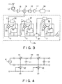
- FIG. 3 is a block diagram of the second preferred embodiment of a receiver including a frequency multiplier circuit according to the present invention.
- the receiver of FIG. 3 can also be included in a single semiconductor chip except for the antenna 11.
- the same reference numbers are given to the same elements as those in FIG. 1, and different points will be mainly described below.
- the receiver of FIG. 3 has the same construction as that in FIG. 1, except that the construction of a local oscillator circuit 14b is different.
- the local oscillator circuit 14b of FIG. 3 comprises: n stages of doubler circuits 2 connected to a source frequency multiplier circuit 1; a filter circuit 31 connected to the output terminal of the first stage doubler circuit 2; and a plurality of phase shift adjusting circuits 32 for adjusting the phase shift quantity of a 90° phase shifter circuit 21 in each of the doubler circuits 2.
- the filter circuit 31 is designed to remove the undesired higher harmonic components included in the output signal of the first stage doubler circuit 2, and the leakage of the input signal of the mixer 22.
- Each of the phase shift adjusting circuits 32 is designed to adjust the phase shift quantity of the 90° phase shifter circuit 21 so that the dc component of the output of the mixer 22 in the corresponding doubler circuits 2 is zero.
- the first stage phase shift adjuster is designed to supply a signal in proportion to a control signal of the corresponding 90° phase shifter circuit to the filter circuit 31 to control the frequency characteristics of the filter circuit 31.
- FIG. 3 has shown an example where the phase shift adjustment of the 90° phase shifter circuit and the control of the frequency characteristics of the filter circuit 31 are carried out on the basis of the output of the mixer 22 in each of the doubler circuits 2, the phase shift quantity of the phase shifter circuit and the frequency characteristics of the filter circuit 31 may be controlled on the basis of a signal other than the output of the mixer 22.
- the filter circuit 31 may also be connected to the output terminal of the second and subsequent stages of doubler circuits 2. In this case, if the filter circuit 31 is connected to the output terminal of the doubler circuit 2 nearer to the first stage, it is possible to more efficiently remove undesired higher harmonic components.
- phase shift quantity of the 90° phase shifter circuit 21 in the doubler circuit 2 is always 90°.
- the phase shift quantity of the 90° phase shifter circuit 21 is not always 90° due to the variation in element and temperature conditions.
- the dc component of the output of the mixer 22 is B( ⁇ /2-x) by expression (2).
- a CR phase shifter circuit using, e.g., the semiconductor element shown in FIG. 4, is considered as the 90° phase shifter circuit 21 capable of adjusting the phase shift quantity.
- the CR phase shifter circuit of FIG. 4 comprises: a reference oscillator 41; a variable resistor R1, the resistance value of which is variably controlled by the quantity of current flowing through a current source 42; a variable resistor R2, the resistance value of which is variably controlled by the quantity of current flowing through a current source 43; capacitors C1 and C2; and an amplifier 44.
- the reference oscillator 41 corresponds to the output of the previous stage doubler circuit 4.
- R can be varied by varying the current I, so that the phase shift quantity can be varied.
- the current quantity I can be set by a current source. If the current quantity I of the current source is controlled by the dc component of the output of the mixer 22, the phase shift quantity can be controlled so that the dc component of the output of the mixer 22 is always zero.
- the CR phase shifter circuit of FIG. 4 can control the value of resistance of the variable resistors by adjusting the current quantity I of the current source. By controlling this value of resistance, the dc component of the output of the mixer 22 can be changed.
- the dc gain of the phase shift adjusting circuit 32 is set to be sufficiently large, and the current quantity I of the current source is changed in accordance with the change of the dc component. That is, assuming that a dc error is ⁇ V and the dc gain of the control circuit is A, the error decreases as A increases since ⁇ V is in proportion to I/A.
- the 90° phase shifter circuit 21 can be controlled so that the dc component of the output of the mixer 22 is always 0, and the phase shift quantity of the 90° phase shifter circuit 21 can be always held to be 90°.
- the output frequencies of the respective stages of the doubler circuits 2 are as follows.
- the 4n order higher harmonic component appears when the phase shift quantity is not held to be 90° .
- various frequency components act on the mixer 22 of the doubler circuit 2.
- the output frequencies of the respective stages of doubler circuits are as follows.
- frequencies adjacent to the finally required frequency of 325.7 MHz are 244.275 MHz and 407.125 MHz, and the difference therebetween is only 81.425 MHz, so that it is difficult to remove these frequencies.
- the reason for this is that the frequency components which are multiples of 81.425 MHz are left in the output of the first stage.
- the output frequency of the respective stages are as follows.
- the frequency component of multiple number of 81.425MHz remains to the third stage output, which is the last stage. That is, the frequencies adjacent to the frequency of 325.7 MHz necessary finally are 244.275 MHz and 407.125MHz. Because the difference between these frequencies is only 81.425 MHz, it is difficult to remove these frequency components.
- the reason why the frequency difference becomes 81.425 MHz is because the frequency component of multiple number of 81.425 MHz is included to the output of the first stage.
- the filter circuit 31 for passing only 81.425 MHz is connected to the output of the first stage to remove the other frequency components, the output frequency of the respective stages are as follows.
- the filter circuit 31 is connected to the output terminal of the first stage doubler circuit 2, frequencies adjacent to 325 MHz are 162.85 MHz and 488.55 MHz, and the difference therebetween is 162.85 MHz, so that it is easy to remove these frequencies.
- the filter circuit 31 for transmitting only a frequency of 162.85 MHz is also provided in the output of the second stage doubler circuit 2, the output frequency of the respective stages are as follows.
- the undesired higher harmonic components outputted from the third stage are greatly removed, and the frequency adjacent to 325 MHz is 651.4 MHz, so that the undesired higher harmonic components can be sufficiently removed.
- the above described filter circuit 31 has a low-pass or band-pass construction for removing higher harmonics, and must be capable of optionally controlling frequency characteristics in accordance with the variation in source oscillation frequency.
- the variation in source oscillation frequency means a case where a system is intended to be used at a frequency which varies due to the difference in system to be used, and a case where the source oscillation frequency slightly varies due to variation of elements, temperature characteristics and so forth.
- the filter circuit 31 of FIG. 5 is a secondary low-pass filter circuit which comprises: a variable resistor R3, the resistance value of which is variably controlled by the quantity of current flowing through a current source 45; a variable resistor R4, the resistance value of which is variably controlled by the quantity of current flowing through a current source 46; amplifiers 47 and 48; and capacitors C3 and C4.
- the dc component of the output of the mixer 22 of the first stage doubler circuit 2 is supplied to the current source. If the current quantity of the current source varies in accordance with the change of the dc component of the output of the mixer 22, the resistance value of the resistor 30 can be varied. This is based on the same concept as that of the resistors R1 and R2 of the CR phase shifter circuit shown in FIG. 4.
- the dc component of the output of the mixer 22 is controlled so that the phase shift quantity based on the CR phase shifter circuit shown in FIG. 4 is actually 90°. That is, this means that the value of resistance of the CR phase shifter circuit settles in such a value that the phase shift quantity is 90° even if the source oscillation frequency is varied.
- the filter circuit 31 comprises the resistors R3 and R4 which have the same constructions as those of the resistors R1 and R2 which are used for the CR phase shifter circuit of FIG. 4 and if the filter circuit 31 is controlled by control signals of the CR phase shifter circuit, the value of resistance settles in the value of resistance capable of always shifting the phase of the source oscillation frequency by 90°. Therefore, if this value is inversely operated to set the capacity of the capacitor so as to decide the frequency characteristics of the filter circuit 31, it is possible to form the filter circuit 31 following the variation in source oscillation frequency.
- the phase shift adjusting circuit 32 is provided for monitoring the output of the mixer 22, and the displacement of the phase shift can be corrected by controlling the phase shift quantity of the 90° phase shifter circuit so that the dc component is always zero. Therefore, even if the phase shift quantity is shifted from 90° due to the variation in element and temperature change, the phase shift quantity can be immediately adjusted, so that the dc component of the output of the mixer 22 can be always zero.
- the filter circuit 31 is provided between the stages of the doubler circuits 2, it is possible to surely inhibit the occurrence of undesired higher harmonics, so that higher harmonic noises are not radiated to the outside of the IC including the receiver in this preferred embodiment. Therefore, it is not required to provide shielding for the frequency multiplier circuit unlike conventional devices, and it is not required to spatially insure the distance between the frequency multiplier circuit and the mixer 22, so that it is possible to easily design the circuit and to miniaturize the circuit.
- the constructions of a 90° phase shifter circuit 21 and a filter circuit 31 are different from those in the second preferred embodiment.
- FIG. 6 is a circuit diagram showing the detailed construction of the third preferred embodiment of a 90° phase shifter circuit 21a according to the present invention.
- the 90° phase shifter circuit 21a of FIG. 6 is a CR phase shifter circuit using a semiconductor element (transistor).
- transistor semiconductor element
- two stages of 45° phase shifting parts (first and second phase shifting parts) 60 for shifting a phase by 45° are cascade-connected to each other.
- the 45° phase shifting parts 60 of FIG. 6 comprises: transistors Q1 and Q2, to the base terminal of which the output of a reference oscillator 41 is supplied; a capacitor C5 which is provided between the emitter terminals of the transistors Q1 and Q2; and current sources 61 and 62 which are connected to the emitter terminals of the transistors Q1 and Q2, respectively.
- the current supplied from the current sources 61 and 62 is controlled by the phase shift adjusting circuit 32 of FIG. 3.
- the current I flowing through the transistors Q1 and Q2 is determined by the current supplied from the current sources 61 and 62. If the current quantity of the current sources 61 and 62 is controlled by the dc component of the output of the mixer 22 of FIG. 3, the phase shift quantity can be adjusted so that the dc component of the output of the mixer 22 is always 0.
- the emitter resistance of the transistors Q1 and Q2 is adjusted by the current quantity of the current sources 61 and 62, and the current quantity of the current sources 61 and 62 is varied in accordance with the change of the dc component of the output of the mixer 22. Specifically, the current quantity of the current sources 61 and 62 is varied so that the dc component of the output of the mixer 22 decreases.
- the 90° phase shifter circuit 21a can be controlled so that the dc component of the output of the mixer 22 is always 0, so that the phase shift quantity can be maintained to be 90°.
- the phase shift quantity is not always 90° due to the variation in element and temperature conditions, and various frequency components act on the mixer of the doubler circuit 2.
- the filter circuit 31 of FIG. 3 has to be constituted of a low-pass or band-pass construction for removing higher harmonics, and must be capable of optionally controlling frequency characteristics in accordance with the variation in source oscillation frequency.
- the variation in source oscillation frequency means a case of intending to use the frequency different in accordance with the used system different from each other, and a case where the source oscillation frequency slightly varies due to the variation in elements, temperature characteristics and so forth.
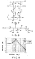
- the filter circuit 31 of FIG. 7 comprises: transistors (first and second variable impedance elements) Q3 and Q4 capable of varying a base-to-emitter resistance; capacitors (first capacitor elements) C6 and C7 which are provided between output terminals OUT1 and OUT2; a transistor (first transistor) Q5 for controlling the voltage of the output terminal OUT1 in accordance with a base-to-emitter current of the transistor Q4; a transistor (second transistor) Q6 for controlling the voltage of the output terminal OUT2 in accordance with a base-to-emitter current of the transistor Q3; a current source 63 which is connected between the emitter and ground terminal of the transistor Q5; a current source 64 which is connected between the emitter and ground terminal of the transistor Q6; and capacitors (second capacitor elements) C8 and C9 which are connected to the emitters of the transistors Q5 and Q6.
- the two capacitors (C6, C7) and the two capacitors (C8, C9) are connected in series, respectively. These capacitors are provided so as to be consistent to the small-signal equivalent circuit diagram of FIG. 8 which will be described later, and the number of the capacitors may be one.
- the current passing through the current sources 63 and 64 is controlled by the output dc component of the mixer 22 in the doubler circuit 2 of FIG. 3. By changing the current passing through the current sources 63 and 64, it is possible to change the emitter resistor of the transistors Q3, Q4, Q5 and Q6. This is the same conception as the resistor of the above CR phase shifter circuit.
- the dc component of the output of the mixer 22 in the double circuit 2 is controlled so that the phase shift quantity based on the CR phase shifter circuit is 90° . That is, this means that the value of resistance of the CR phase shifter circuit always settles in such a value of resistance that the quantity can be phase-shifted by 90° even if the source oscillation frequency is varied on various conditions.
- the filter circuit 31 comprises an emitter resistor which has the same construction as that of the emitter resistor of the transistor in the CR phase shifter circuit and if the filter circuit 31 is controlled by control signals of the CR phase shifter circuit, the value of resistance settles in the emitter resistance capable of always shifting the phase of the source oscillation frequency by 90°. Therefore, if this value is inversely operated to set the capacity of the capacitor so as to decide the frequency characteristics of the filter circuit 31, it is possible to form the filter circuit 31 following the variation in source oscillation frequency.
- the emitter resistors of the transistors Q3, Q4 and transistors Q5, Q6 are expressed by variable resistors (first and second variable impedance elements) re, and the transistors Q5, Q6 are expressed by a buffer 81. Since the base and collector of the transistors Q5, Q6 are crossed, the same current as the output current Io of the buffer 81 flows through a constant current source (current supply circuit) 82. Moreover, the capacitors C6, C7 of FIG. 7 are expressed by a capacitor (first capacitor element) C11, and the capacitors C8, C9 are expressed by a capacitor C12.
- T(s) (1 + s x C12 x re) / (1 - ( ⁇ x re) ⁇ 2 x C11 x C12 + s x (C11 x re + C12 x re - C12 x re) (7)
- FIG. 9 is a graph expressed by expression (7), wherein the axis of abscissas denotes frequency (standardized at the central frequency) and the axis of ordinates denotes amplitude (expressed by logarithm).
- Q is determined by the ratio C11/C12 of the capacitance C11 to the capacitance C12, and Q is high when the value of C11/C12 is small.
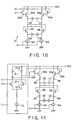
- FIG. 10 shows a filter circuit 31 wherein the transistors Q3 and Q4 of FIG. 7 are Darlington-connected.
- the resistance of the input side viewed from the emitters of the transistors Q3 and Q4 is 2 x re, and a linearly operation range is ⁇ 2VT (about ⁇ 52 mV) in differential.
- FIG. 11 shows a filter circuit 31 used for an actual LSI or the like.
- the dc voltage error generated by the filter circuit 31 of FIG. 11 is usually about 1 mv, and the required signal level must be sufficiently higher than the dc error voltage.
- the filter circuit 31 of FIG. 11 is characterized in that a limiter amplifier (first limiter amplifier) 71 is provided between the input terminal and transistors Q3, Q4 of PIG. 7.
- a linearly operating range is ⁇ 2 VT (about ⁇ 52 mV), and is not sufficiently greater than the dc error voltage 1 mv. Therefore, in order to obtain an operating range which is sufficiently greater than the dc error voltage, it is required to operate the filter circuit 31 in a non-linear range. Since the dc error voltage should be 1 % or less, the input signal level should be usually 100 mV. However, when the filter circuit 31 is operated in a non-linear range, the frequency characteristics of the filter circuit 31 are varied by the input signal level, so that the limiter amplifier 71 of FIG. 11 is required.
- the frequency characteristics of the filter circuit 31 of FIG. 11 must be controlled in accordance with the phase shift quantity of the 90° phase shifter circuit 21a. However, when there is a fixed phase shift quantity based on a limiter amplifier 26 provided in the 90° phase shifter circuit 21a, the frequency characteristics of the filter circuit 31 are shifted by a value corresponding to the fixed phase shift quantity. This means that the frequency characteristics of the filter circuit 31 can not faithfully follow the phase shift quantity of the 90° phase shifter circuit 21a if the source oscillation frequency varies, so that required signals are attenuated.
- the filter circuit 31 of FIG. 11 is provided with a fixed resistor (first impedance element) R5 between the emitter of the transistor Q3 and the collector of the transistor Q5, a fixed resistor (second impedance element) R6 between the emitter of the transistor Q4 and the collector of the transistor Q6, a fixed resistor (third impedance element ) R7 between the emitter of the transistor Q5 and the current source 63, and a fixed resistor (fourth impedance element) R8 between the emitter of the transistor Q6 and the resistor R8.
- the fixed phase shift quantity caused by the limiter amplifier 26 is canceled, so that it is possible to realize the filter circuit 31 faithfully following the phase shift quantity of the 90° phase shifter circuit.
- the fixed resistors R5 and R6 are expressed by an expression wherein 2re is substituted for re in expression (9).
- the linearly operating range is ⁇ 2VT (about ⁇ 52 mV) which is not sufficiently greater than the dc error voltage of 1 mV. Therefore, in order to obtain a sufficiently greater operating range than the dc error voltage, it is required to operate the filter circuit 31 in a non-linear range. Since the dc error voltage should be 1 % or less, the input signal level should be usually 100 mV. However, when the filter circuit 31 is operated in the non-linear range, it is required to provide the limiter amplifier 71 since the frequency characteristics of the filter circuit 31 is varied by the input signal level.
- FIG. 12 is a circuit diagram of a 90° phase shifter circuit 21a having a limiter amplifier 26. By this circuit, it is possible to obtain a sufficiently great input signal level with respect to the dc voltage error.
- the filter circuit 31 in order to cancel the fixed phase shift quantity, which is caused by the limiter amplifier 26 of the 90° phase shifter 21a, by the resistors R6 through R8 provided in the filter circuit 31, it is possible to realize the filter circuit 31 capable of controlling the frequency characteristics faithfully following the phase shift quantity of the 90° phase shifter circuit 21a. Thus, even if adjacent undesired high frequencies are generated, the filter circuit 31 can attenuate undesired frequencies.
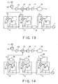
- FIG. 3 has shown the local oscillator circuit 14b having both of the filter circuit 31 and the phase shift adjusting circuit 32, a local oscillator circuit 14b having a filter circuit 31 and no phase shift adjusting circuit 32 as shown in FIG. 13, and a local oscillator circuit 14b having a phase shift adjusting circuit 32 and no filter circuit 31 as shown in FIG. 14 are considered.
- undesired frequency components appear if the phase shift quantity in the 90° phase shifter circuit 21 is not correctly held to be 90°.
- the signal level of the undesired frequency components is doubled every time passing through the doubler circuit 2.
- the signal level of a required frequency is 0 dB
- the signal level of adjacent undesired frequencies is increased by 6 dB every time passing through one stage doubler circuit 2. Because of this, the required frequency is easily interfered by the undesired frequencies, and the receiving sensitivity deteriorates, so that communication quality deteriorates. Therefore, it is difficult to realize commercialization of products.
- the mixer 22 has two input terminals. If signals f1 and f2 are inputted to these input terminals, the mixer 22 outputs a frequency signal of
- . If the signals f1 and f2 contain even order distorted components 2n ⁇ f (n is an integer which is 0 or more), the mixer 22 outputs a frequency signal of (2n ⁇ f) ⁇ f (2n ⁇ 1) ⁇ f. Therefore, the frequency component of (2n+1) ⁇ f remains in the output of the doubler circuit 2.
- phase shift adjusting circuit itself generates a DC offset by the frequency component of 4 ⁇ f included in the output signal of the mixer 22, so that it is difficult to remove the DC offset.
- phase shift can not be maintained to be correctly 90° , and the frequency component of 4 ⁇ f contained in the output of the mixer 22 can not be removed.
- the fourth preferred embodiment which will be described later is characterized in that spurious contained in the source oscillation signal from the source oscillator circuit 1 is removed, and the distorted component contained in the input signal of the mixer 22 is removed, and the distorted component contained in the output signal of the mixer 22 is removed.
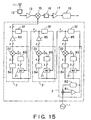
- FIG. 15 is a block diagram of the fourth preferred embodiment of a receiver including a frequency multiplier circuit according to the present invention.
- the receiver of FIG. 15 has the same construction as that in FIG. 3, except that the internal construction of the doubler circuit in the local oscillator circuit 14 is different from that in FIG. 3.
- FIG. 16 is an enlarged block diagram of the internal construction of the first stage doubler circuit 2.
- the first stage doubler circuit 2 comprises: a limiter amplifier (first waveform shaping circuit) 81 for shaping the waveform of a source oscillation signal from the source oscillation circuit 1; an offset cancel circuit 82 for removing a DC offset, which is contained in the output of the limiter amplifier 81, to feed the output back to the input side of the limiter amplifier 81; a 90° phase shifter circuit 21 for shifting the phase of the output signal of the limiter amplifier 81 by 90° ; a limiter amplifier (fourth waveform shaping circuit) 83 for shaping the waveform of the output of the 90° phase shifter circuit 21; a limiter amplifier (third waveform shaping circuit) 84 for shaping the waveform of the output of the limiter amplifier 81; and a mixer 22 for generating a doubled signal on the basis of the output
- first waveform shaping circuit for shaping the waveform of a source oscillation signal from the source oscillation circuit 1
- the doubler circuits 2 other than the first stage in FIG. 15 have a construction wherein the limiter amplifier 81 and the offset cancel circuit 82 are omitted from the first stage doubler circuit.
- the limiter amplifier 81 is designed to remove the even order distorted components contained in the source oscillation signal from the source oscillator circuit 1, and the offset cancel circuit 82 is designed to remove the DC offset contained in the output of the limiter amplifier 81.
- a complete rectangular wave having a duty ratio of 50 % is inputted to the 90° phase shifter circuit 21.
- FIG. 3 Since the above described construction of FIG. 3 can not remove the even order frequency components contained in the source oscillation signal from the source oscillator circuit 1, there is the possibility that odd order ((2n+1) x f) spurious of multiplied output may be generated in the output of the mixer 22.
- FIG. 15 since the construction of FIG. 15 is designed to carry out a multiplication processing after changing the source oscillation signal to a complete rectangular wave having a duty ratio of 50 %, spurious is not generated in the output of the mixer 22.
- FIG. 17 is a circuit diagram showing the detailed construction of the phase shift adjusting circuit of FIG. 16.
- the offset cancel circuit 82 of FIG. 17 comprises: a differential amplifier having transistors Q21 and Q22 for comparing offset voltages of differential input signals, and a current source 86; a current mirror circuit having transistors (Q23, Q24), (Q25, Q26), (Q27, Q28) connected to the differential amplifier; a capacitor C21 for removing ac components from the output of the differential amplifier; and a transistor Q29 for current-outputting the output of the differential amplifier.
- the capacitor C21 and the transistor Q28 constitute a low-pass filter.
- FIG. 18 is a circuit diagram showing the detailed construction of the limiter amplifier of FIG. 16.
- the limiter amplifier of FIG. 18 comprises: a differential amplifier having transistors Q30 and Q31, resistors R21 and R22 and a current source 87; capacitors C22 and C23 connected to the resistors R21 and R22 in parallel, respectively; and an emitter follower circuit having transistors Q32 and Q33 connected to the output of the differential amplifier.
- the capacitors C22 and C23 and the resistors R21 and R22 constitute a low-pass filter.
- the low-pass filters of FIGS. 17 and 18 are not always essential constructions, but it is possible to reduce higher order spurious by providing the low-pass filters.
- phase shift quantity of the 90° phase shifter circuit 21 is shifted from 90° in the doubler circuit 2 of FIG. 16, a frequency component of 4 ⁇ f appears in the output of the mixer 22. This frequency component is changed to a DC offset by the limiter amplifier 85, and the DC offset is removed by the phase shift adjusting circuit 32.
- the distorted component is changed to a DC component by the limiter amplifier 85. Therefore, the distorted component is not inputted to the phase shift adjusting circuit 32, and no tertiary intermodulation is generated.
- one of the input signals contains frequency components of f (0° ) and 3f(0° ), and the other input signal contains frequency components of f(90° ) and 3f((270° )).
- the frequency component of 4 ⁇ f can be canceled when two input signals to the mixer 22 have the same waveform, i.e., only when two input signals to the mixer 22 have the same level as that of the phase of the tertiary component.
- low-pass filters are provided in the limiter amplifiers 81 and 83 through 85 for attenuating high order components.
- the distorted components contained in the input signals of the doubler circuits 2 and the output signals of the 90° phase shifter circuit 21 are changed to DC offsets by the limiter amplifiers 83 and 84 and then inputted to the mixer 22. Therefore, even if the input signals of the mixer 22 contain even order components, it is possible to inhibit the occurrence of odd order ((2n+1) x f) spurious components of multiplied outputs passing though the output of the mixer 22.
- a band-pass filter may be provided between the mixer 22 and the limiter amplifier 85 although this is not shown in FIG. 15.
- spurious contained in the output of the mixer 22 Even if spurious is generated in the band-pass filter itself, it is possible to remove the spurious by the subsequent stage limiter amplifier 85 and offset cancel circuit 82.
Landscapes
- Superheterodyne Receivers (AREA)
- Oscillators With Electromechanical Resonators (AREA)
- Networks Using Active Elements (AREA)
- Manipulation Of Pulses (AREA)
- Inductance-Capacitance Distribution Constants And Capacitance-Resistance Oscillators (AREA)
Claims (17)
- Eine Frequenzmultipliziererschaltung, umfassend:wobei die 90° Phasenschiebeschaltung umfasst:eine Quellenoszillator, der konfiguriert ist, ein Quellenoszillatorsignal unter Verwendung eines Kristalloszillators zu erzeugen;n Frequenzmultipliziererschaltungen (n ist eine ganze Zahl, gleich oder größer 2), von denen jede eine 90° Phasenschiebeschaltung umfasst, konfiguriert zur Verschiebung der Phase eines Eingangssignals um 90°, und einen Mischer, konfiguriert zur Erzeugung eines gedoppelten Signals des Eingangssignals auf Grundlage des Eingangssignals und eines Ausgangssignals der 90° Phasenschiebeschaltung, wobei die n Frequenzmultipliziererschaltungen in einer Kaskade verbunden sind, das Quellenoszillatorsignal in eine Frequenzmultipliziererschaltung einer ersten Stufe der n Frequenzmultipliziererschaltungen eingegeben wird, und eine Frequenzmultipliziererschaltung einer letzten Stufe der n Frequenzmultipliziererschaltungen ein Signal ausgibt, das eine Frequenz aufweist, die 2n mal so hoch ist, wie die Frequenz des Quellenoszillatorsignal; undmindestens eine Phasenschiebeeinstellschaltung, bereitgestellt, so dass sie zumindest einem Teil der n Frequenzmultipliziererschaltungen entspricht, wobei die Phasenschiebeeinstellschaltung die Phasenschiebegröße einer entsprechenden der 90° Phasenschieberschaltungen einstellt, so dass die Ausgangsgleichspannung eines entsprechenden der Mischer im wesentlichen Null ist,eine erste Stromquelle, geeignet für ein Einstellen einer Stromgröße durch die Ausgabe der Phasenschiebeeinstellschaltung; undein erstes Impedanzelement, wobei die Impedanz variabel in Übereinstimmung mit einer durch die Stromquelle fließenden Stromgröße eingestellt wird.
- Eine Frequenzmultipliziererschaltung nach Anspruch 1, die weiter mindestens eine Filterschaltung umfasst, bereitgestellt zwischen zwei benachbarten von mindestens einem Teil der Stufen der n Frequenzmultipliziererschaltungen, konfiguriert zur Entfernung unerwünschter Frequenzkomponenten,
wobei die Phasenschiebeeinstellschaltung dazu ausgebildet ist, eine Bandcharakteristik einer entsprechenden der Filterschaltungen so einzustellen, dass die Ausgangsgleichspannung eines entsprechenden der Mischer Null ist. - Eine Frequenzmultipliziererschaltung nach Anspruch 2, wobei die Filterschaltung umfasst:eine zweite Stromquelle, dazu geeignet, eine Stromgröße durch die Ausgabe der Phasenschiebereinstellschaltung einzustellen; undein zweites Impedanzelement, wobei eine Impedanz variabel in Übereinstimmung mit einer durch die zweite Stromquelle fließenden Stromgröße eingestellt wird.
- Eine Frequenzmultipliziererschaltung nach Anspruch 2, wobei die Filterschaltung umfasst:ein erstes variables Impedanzelement, das zwischen einem Eingangsanschluss und einem Ausgangsanschluss angeschlossen ist, und das eine Impedanz mittels Strömen variieren kann;ein erstes Kondensatorelement, das mit dem Ausgangsanschluss verbunden ist;ein zweites variables Impedanzelement, dazu ausgebildet, eine Spannung des Ausgangsanschlusses in Übereinstimmung mit Strömen zu steuern; undeine Stromversorgungsschaltung, dazu ausgebildet, einen Strom, der die gleiche Phase wie die eines durch das zweite variable Impedanzelement fließendem Stromes aufweist, durch den Ausgangsanschluss zu führen.
- Eine Frequenzmultiplizierschaltung nach Anspruch 2, wobei die Filterschaltung umfasst:wobei der erste Transistor einen Strom, der die gleiche Phase wie die eines durch den zweiten Transistor fließenden Stromes aufweist, durch den ersten Ausgangsanschluss führt, undein erstes variables Impedanzelement, das zwischen einem ersten Eingangsanschluss und einem ersten Ausgangsanschluss angeschlossen ist, und wobei eine Impedanz variabel durch einen durch den ersten Eingangsanschluss fließenden Strom gesteuert wird;ein zweites variables Impedanzelement, das zwischen einem zweiten Eingangsanschluss und einem zweiten Ausgangsanschluss angeschlossen ist, und wobei eine Impedanz variabel durch einen durch den zweiten Eingangsanschluss fließenden Strom gesteuert wird,ein erstes Kondensatorelement, dass zwischen den ersten und zweiten Ausgangsanschluss angeschlossen ist;einen ersten Transistor, dazu angeordnet, eine Spannung des ersten Ausgangsanschlusses zu steuern;einen zweiten Transistor, dazu ausgebildet, eine Spannung des zweiten Ausgangsanschlusses zu steuern; undein zweites Kondensatorelement, das zwischen den Ausgangsanschlüssen eines jeden des ersten und zweiten Transistors angeschlossen ist,
der zweite Transistor einen Strom, der die gleiche Phase wie die eines durch den ersten Transistor fließenden Stromes aufweist, durch den zweiten Ausgangsanschluss führt. - Eine Frequenzmultiplizierschaltung nach Anspruch 5, wobei mindestens eines des ersten bis vierten variablen Impedanzelements einen Bipolartransistor umfasst, dazu ausgebildet, variabel eine Impedanz durch ein Steuern eines durch einen Emitteranschluss des Bipolartransistor fließenden Stromes zu steuern.
- Eine Frequenzmultipliziererschaltung nach Anspruch 6, wobei mindestens eines des ersten bis vierten variablen Impedanzelements eine Vielzahl von Bipolartransistoren umfasst, die in einer Darlington-Verbindung angeschlossen sind.
- Eine Frequenzmultipliziererschaltung nach Anspruch 4, wobei die Filterschaltung weiter einen ersten Begrenzerverstärker umfasst, zwischen dem ersten und zweiten Eingangsanschluss und dem ersten und zweiten variablen Impedanzelement angeschlossen, dazu ausgebildet, eine Spannungsamplitude eines Eingangssignals auf einen vorgegebenen Spannungsbereich zu begrenzen, und um das begrenzte Signal auszugeben, und wobei die 90° Phasenschiebeschaltung umfasst:einen ersten und zweiten Phasenschiebeabschnitt, miteinander in einer Kaskade verbunden, dazu ausgebildet, die Phase von Eingangssignalen um im wesentlichen 45° zu verschieben, und um die Phasen verschobenen Signale auszugeben;eine zweite Begrenzerschaltung, mit der flussaufwärtigen Seite des ersten Phasenschiebeabschnitts verbunden, dazu ausgebildet, eine Spannungsamplitude eines Eingangssignals auf eine vorgegebene Spannung zu begrenzen, und um das begrenzte Signal auszugeben; undeine dritte Begrenzerschaltung, zwischen dem zweiten Begrenzerverstärker und dem zweiten Phasenschieberabschnitt angeschlossen, und dazu ausgebildet, eine Spannungsamplitude eines Ausgangssignals des ersten Phasenschieberabschnitts auf einen vorgegebenen Spannungsbereich zu begrenzen, und um das begrenzte Signal auszugeben.
- Eine Frequenzmultipliziererschaltung nach Anspruch 5, wobei die Filterschaltung umfasst:ein erstes Impedanzelement, das zwischen dem ersten variablen Impedanzelement und dem ersten Ausgangsanschluss angeschlossen ist;ein zweites Impedanzelement, das zwischen dem zweiten variablen Impedanzelement und dem zweiten Ausgangsanschluss angeschlossen ist;ein drittes Impedanzelement, dass mit dem ersten Transistor und dem zweiten Kondensatorelement verbunden ist; undein viertes Impedanzelement, dass zwischen dem zweiten Transistor und dem zweiten Kondensatorelement angeschlossen ist.
- Eine Frequenzmultiplizererschaltung nach Anspruch 2, wobei die Filterschaltung zumindest zwischen der ersten und zweiten Stufe der Frequenzmultipliziererschaltungen bereitgestellt ist.
- Eine Frequenzmultipliziererschaltung nach Anspruch 1, die weiter umfasst:eine Lokaloszillatorschaltung, dazu ausgebildet, ein lokales Oszillationssignal zu erzeugen, wobei die Lokaloszillatorschaltung den Quellenoszillator und die n Frequenzmultipliziererschaltungen aufweist,einen Zwischenfrequenzsignalkonverter, dazu ausgebildet, ein Hochfrequenzsignal, empfangen durch eine Antenne, auf Grundlage des lokalen Oszillationssignals in ein Zwischenfrequenzsignal umzuwandeln; undeinen Demodulator, der dazu ausgebildet ist, eine Demuodulationsverarbeitung auf Grundlage des Zwischenfrequenzsignals durchzuführen.
- Eine Frequenzmultipliziererschaltung nach Anspruch 1, wobei eine Frequenzmultipliziererschaltung einer ersten Stufe der n Frequenzmultipliziererschaltungen umfasst:eine Signalformungsschaltung, dazu ausgebildet, die Signalform des durch den Quellenoszillator erzeugten Quellenoszillatorsignals zu formen; undeine Versatzausgleichsschaltung, ausgebildet zur Entfernung einer Ausgangsgleichspannungskomponente der ersten Signalformungsschaltung.
- Eine Frequenzmultipliziererschaltung nach Anspruch 1, die weiter umfasst:wobei die Signalformungsschaltung die Signalform eines Ausgangssignals des Mischers formt, undmindestens eine Signalformungsschaltung und mindestens eine Phasenschiebeeinstellschaltung, die so bereitgestellt sind, dass sie mindestens einem Teil der Frequenzmultipliziererschaltungen der n Frequenzmultipliziererschaltungen entsprechen,
die Phasenschiebeeinstellschaltung eine Phasenschiebegröße einer entsprechenden einer der 90° Phasenschiebeschaltungen einstellt. - Eine Frequenzmultipliziererschaltung nach Anspruch 1, weiter umfassend:wobei die erste Signalformungsschaltung die Signal form des Eingangssignals formt,eine erste und zweite Signalformungsschaltung und eine Phasenschiebeeinstellschaltung, die so bereitgestellt sind, dass sie mindestens einem Teil von Frequenzmultipliziererschaltungen der n Frequenzmultiplizierschaltungen entsprechen,
die zweite Signalformungsschaltung ein Ausgangssignals der 90° Phasenschiebeschaltung phast, und
der Mischer ein gedoppeltes Signal aus dem Eingangssignal erzeugt, auf Grundlage eines jeden von Ausgangssignalen der ersten und zweiten Signalformungsschaltung. - Eine Frequenzmultipliziererschaltung nach Anspruch 12, wobei die erste Signalformungsschaltung einen Begrenzerverstärker und einen Tiefpassfilter umfasst.
- Eine Frequenzmultipliziererschaltung nach Anspruch 13, wobei die Signalformungsschaltung einen Begrenzerverstärker und einen Tiefpassfilter umfasst.
- Eine Frequenzmultiplizererschaltung nach Anspruch 14, wobei mindestens eine der ersten und zweiten Signalformungsschaltung einen Begrenzerverstärker und einen Tiefpassfilter umfasst.
Applications Claiming Priority (4)
| Application Number | Priority Date | Filing Date | Title |
|---|---|---|---|
| JP2000127087 | 2000-04-27 | ||
| JP2000127087 | 2000-04-27 | ||
| JP2000364648A JP3977591B2 (ja) | 2000-04-27 | 2000-11-30 | 周波数逓倍回路および半導体集積回路 |
| JP2000364648 | 2000-11-30 |
Publications (3)
| Publication Number | Publication Date |
|---|---|
| EP1156581A2 EP1156581A2 (de) | 2001-11-21 |
| EP1156581A3 EP1156581A3 (de) | 2002-09-04 |
| EP1156581B1 true EP1156581B1 (de) | 2004-10-13 |
Family
ID=26590931
Family Applications (1)
| Application Number | Title | Priority Date | Filing Date |
|---|---|---|---|
| EP01110058A Expired - Lifetime EP1156581B1 (de) | 2000-04-27 | 2001-04-27 | Frequenzmultiplizierende Schaltung und integrierte Halbleiterschaltung |
Country Status (6)
| Country | Link |
|---|---|
| US (1) | US6456143B2 (de) |
| EP (1) | EP1156581B1 (de) |
| JP (1) | JP3977591B2 (de) |
| KR (1) | KR100398014B1 (de) |
| CN (1) | CN1168198C (de) |
| DE (1) | DE60106326T2 (de) |
Families Citing this family (25)
| Publication number | Priority date | Publication date | Assignee | Title |
|---|---|---|---|---|
| GB2378593B (en) * | 2001-08-03 | 2003-09-17 | Zarlink Semiconductor Ltd | A frequency doubler circuit arrangement |
| DE10158357A1 (de) * | 2001-11-28 | 2003-06-12 | Philips Intellectual Property | Kompensationsschaltung für Frequenzfilter |
| US7324561B1 (en) | 2003-06-13 | 2008-01-29 | Silicon Clocks Inc. | Systems and methods for generating an output oscillation signal with low jitter |
| US7098753B1 (en) | 2003-06-13 | 2006-08-29 | Silicon Clocks, Inc. | Oscillator with variable reference |
| JP2005012648A (ja) * | 2003-06-20 | 2005-01-13 | Toshiba Corp | 無線通信装置及びその送受信回路 |
| TW200518484A (en) * | 2003-11-26 | 2005-06-01 | Niigata Seimitsu Co Ltd | AM/FM radio receiver and local oscillation circuit using the same |
| EP1698046B1 (de) * | 2003-12-19 | 2014-03-19 | TELEFONAKTIEBOLAGET LM ERICSSON (publ) | Frequenzvervielfachungsanordnungen und verfahren zur frequenzvervielfachung |
| US20060132248A1 (en) * | 2004-12-16 | 2006-06-22 | Nel Frequency Controls, Inc. | Bulk acoustic wave crystal controlled clock with surface acoustic wave filter multiplier |
| CN100456630C (zh) * | 2005-03-22 | 2009-01-28 | 杭州华三通信技术有限公司 | 低频时钟信号产生方法及低频时钟信号产生装置 |
| JP4631673B2 (ja) * | 2005-07-27 | 2011-02-16 | カシオ計算機株式会社 | 電波受信装置、電波受信回路及び電波時計 |
| KR100745039B1 (ko) | 2006-05-18 | 2007-08-01 | 세원텔레텍 주식회사 | 2,3,4차 주파수 체배기 및 그 설계방법 |
| EP2120340A4 (de) * | 2007-03-06 | 2012-10-24 | Fujitsu Ltd | Phasenschieber |
| US8275817B2 (en) * | 2007-04-19 | 2012-09-25 | General Instrument Corporation | Broadband low noise complex frequency multipliers |
| US7495484B1 (en) * | 2007-07-30 | 2009-02-24 | General Instrument Corporation | Programmable frequency multiplier |
| US8369820B2 (en) * | 2007-09-05 | 2013-02-05 | General Instrument Corporation | Frequency multiplier device |
| KR100932533B1 (ko) * | 2007-12-11 | 2009-12-17 | 엘아이지넥스원 주식회사 | 지령 수신기용 쿠밴드 송수신 장치 |
| JP5067294B2 (ja) * | 2008-07-17 | 2012-11-07 | パナソニック株式会社 | 電波受信装置 |
| CN102545826B (zh) * | 2010-12-10 | 2016-03-30 | 上海卫星工程研究所 | 卫星用二次变频接收机的本振频率源 |
| WO2013096266A1 (en) * | 2011-12-20 | 2013-06-27 | University Of Florida Research Foundation, Inc. | Systems and methods of local oscillator distribution and phase shifting |
| JP5553463B1 (ja) * | 2014-03-13 | 2014-07-16 | 株式会社ソニック | パルス圧縮超音波探知装置 |
| CN104767488B (zh) * | 2015-04-29 | 2017-12-19 | 中国科学院微电子研究所 | 一种基于晶体振荡器电路的倍频装置 |
| JP6671151B2 (ja) * | 2015-11-09 | 2020-03-25 | セイコーエプソン株式会社 | 物理量検出回路、電子機器および移動体 |
| CN107634722A (zh) * | 2017-09-27 | 2018-01-26 | 杭州暖芯迦电子科技有限公司 | 一种用于毫米波lo发生器的频率倍频器及其方法 |
| CN109655841B (zh) * | 2018-12-13 | 2020-08-14 | 北京遥测技术研究所 | 太赫兹多模实时成像系统 |
| KR102543233B1 (ko) | 2020-05-19 | 2023-06-14 | 한국전자통신연구원 | 주파수 체배 장치 및 주파수 체배 방법 |
Citations (1)
| Publication number | Priority date | Publication date | Assignee | Title |
|---|---|---|---|---|
| EP0612189A2 (de) * | 1993-02-15 | 1994-08-24 | Samsung Electronics Co., Ltd. | Frequenzmultiplikator |
Family Cites Families (9)
| Publication number | Priority date | Publication date | Assignee | Title |
|---|---|---|---|---|
| US4956797A (en) * | 1988-07-14 | 1990-09-11 | Siemens Transmission Systems, Inc. | Frequency multiplier |
| US5077546A (en) * | 1990-11-07 | 1991-12-31 | General Electric Company | Low phase noise frequency multiplier |
| US5436938A (en) * | 1993-08-19 | 1995-07-25 | Northern Telecom Limited | Phase error detector for a phase locked loop |
| JPH07235837A (ja) | 1994-02-24 | 1995-09-05 | Toshiba Corp | 2逓倍回路 |
| GB2317769B (en) * | 1996-09-27 | 2000-10-11 | Marconi Gec Ltd | Radar systems |
| JPH10126156A (ja) | 1996-10-22 | 1998-05-15 | Japan Radio Co Ltd | 逓倍器 |
| KR100230807B1 (ko) * | 1996-12-23 | 1999-11-15 | 김영환 | 펄스폭 제어가 가능한 주파수 체배기 |
| US5963071A (en) * | 1998-01-22 | 1999-10-05 | Nanoamp Solutions, Inc. | Frequency doubler with adjustable duty cycle |
| JP3592950B2 (ja) * | 1999-03-11 | 2004-11-24 | 株式会社東芝 | 周波数逓倍回路 |
-
2000
- 2000-11-30 JP JP2000364648A patent/JP3977591B2/ja not_active Expired - Fee Related
-
2001
- 2001-04-26 KR KR10-2001-0022641A patent/KR100398014B1/ko not_active Expired - Fee Related
- 2001-04-27 DE DE60106326T patent/DE60106326T2/de not_active Expired - Lifetime
- 2001-04-27 US US09/842,807 patent/US6456143B2/en not_active Expired - Lifetime
- 2001-04-27 CN CNB011171596A patent/CN1168198C/zh not_active Expired - Fee Related
- 2001-04-27 EP EP01110058A patent/EP1156581B1/de not_active Expired - Lifetime
Patent Citations (1)
| Publication number | Priority date | Publication date | Assignee | Title |
|---|---|---|---|---|
| EP0612189A2 (de) * | 1993-02-15 | 1994-08-24 | Samsung Electronics Co., Ltd. | Frequenzmultiplikator |
Also Published As
| Publication number | Publication date |
|---|---|
| JP2002016440A (ja) | 2002-01-18 |
| CN1168198C (zh) | 2004-09-22 |
| JP3977591B2 (ja) | 2007-09-19 |
| KR100398014B1 (ko) | 2003-09-19 |
| US6456143B2 (en) | 2002-09-24 |
| DE60106326D1 (de) | 2004-11-18 |
| EP1156581A2 (de) | 2001-11-21 |
| CN1326264A (zh) | 2001-12-12 |
| EP1156581A3 (de) | 2002-09-04 |
| KR20010098905A (ko) | 2001-11-08 |
| US20010043109A1 (en) | 2001-11-22 |
| DE60106326T2 (de) | 2006-02-23 |
Similar Documents
| Publication | Publication Date | Title |
|---|---|---|
| EP1156581B1 (de) | Frequenzmultiplizierende Schaltung und integrierte Halbleiterschaltung | |
| US6404293B1 (en) | Adaptive radio transceiver with a local oscillator | |
| US6057723A (en) | Phase shifter | |
| Stetzler et al. | A 2.7-4.5 V single chip GSM transceiver RF integrated circuit | |
| US6020783A (en) | RF notch filter having multiple notch and variable notch frequency characteristics | |
| JP3666686B2 (ja) | 時分割ミクサ回路 | |
| US6625436B1 (en) | Radio receivers | |
| US6324388B1 (en) | Image reject mixer circuit arrangements | |
| WO1991003882A1 (en) | Image canceling mixer circuit on an integrated circuit chip | |
| JP4083116B2 (ja) | 低漏洩局部発振器システム | |
| JPS62500556A (ja) | 周波数変調信号を少なくとも一つの中間周波数を経て低周波信号に変換するための方法及び回路装置 | |
| GB2342520A (en) | Frequency selection in a receiver in which unwanted signals are selected by filtering and fed back to be subtracted from the input | |
| EP1236285B1 (de) | Empfängerschaltung | |
| KR20040014661A (ko) | 고조파 믹서 | |
| EP1751846B1 (de) | Gegenüber störungen robuster xo-puffer | |
| US20050143039A1 (en) | Image rejection quadratic filter | |
| US5784692A (en) | Method and apparatus for generating non-linear variable impedance | |
| KR100394913B1 (ko) | 필터를 갖춘 회로 장치 및 상기 회로 장치의 작동 방법 | |
| JP2000013146A (ja) | ミクサ―回路装置 | |
| US6091306A (en) | Circuit configuration with main and subordinate oscillators | |
| EP1206839B1 (de) | Phasenverschiebungsanordnung | |
| US20110105057A1 (en) | Harmonic generation of a fundamental frequency system and method | |
| Phang | On-Chip Image Reject Techniques for Wireless Receivers | |
| GB2350953A (en) | Harmonic reduction in a receiver using a variable mark-to-space ratio in a demodulator oscillator | |
| JP2000078047A (ja) | 受信機 |
Legal Events
| Date | Code | Title | Description |
|---|---|---|---|
| PUAI | Public reference made under article 153(3) epc to a published international application that has entered the european phase |
Free format text: ORIGINAL CODE: 0009012 |
|
| 17P | Request for examination filed |
Effective date: 20010427 |
|
| AK | Designated contracting states |
Kind code of ref document: A2 Designated state(s): AT BE CH CY DE DK ES FI FR GB GR IE IT LI LU MC NL PT SE TR |
|
| AX | Request for extension of the european patent |
Free format text: AL;LT;LV;MK;RO;SI |
|
| PUAL | Search report despatched |
Free format text: ORIGINAL CODE: 0009013 |
|
| AK | Designated contracting states |
Kind code of ref document: A3 Designated state(s): AT BE CH CY DE DK ES FI FR GB GR IE IT LI LU MC NL PT SE TR |
|
| AX | Request for extension of the european patent |
Free format text: AL;LT;LV;MK;RO;SI |
|
| RIC1 | Information provided on ipc code assigned before grant |
Free format text: 7H 03B 21/04 A, 7H 03B 21/01 B, 7H 03B 19/14 B |
|
| AKX | Designation fees paid |
Designated state(s): DE FR GB |
|
| 17Q | First examination report despatched |
Effective date: 20030915 |
|
| GRAP | Despatch of communication of intention to grant a patent |
Free format text: ORIGINAL CODE: EPIDOSNIGR1 |
|
| GRAS | Grant fee paid |
Free format text: ORIGINAL CODE: EPIDOSNIGR3 |
|
| GRAA | (expected) grant |
Free format text: ORIGINAL CODE: 0009210 |
|
| AK | Designated contracting states |
Kind code of ref document: B1 Designated state(s): DE FR GB |
|
| PG25 | Lapsed in a contracting state [announced via postgrant information from national office to epo] |
Ref country code: FR Free format text: LAPSE BECAUSE OF FAILURE TO SUBMIT A TRANSLATION OF THE DESCRIPTION OR TO PAY THE FEE WITHIN THE PRESCRIBED TIME-LIMIT Effective date: 20041013 |
|
| REG | Reference to a national code |
Ref country code: GB Ref legal event code: FG4D |
|
| REG | Reference to a national code |
Ref country code: IE Ref legal event code: FG4D |
|
| REF | Corresponds to: |
Ref document number: 60106326 Country of ref document: DE Date of ref document: 20041118 Kind code of ref document: P |
|
| PG25 | Lapsed in a contracting state [announced via postgrant information from national office to epo] |
Ref country code: GB Free format text: LAPSE BECAUSE OF NON-PAYMENT OF DUE FEES Effective date: 20050427 |
|
| PLBE | No opposition filed within time limit |
Free format text: ORIGINAL CODE: 0009261 |
|
| STAA | Information on the status of an ep patent application or granted ep patent |
Free format text: STATUS: NO OPPOSITION FILED WITHIN TIME LIMIT |
|
| 26N | No opposition filed |
Effective date: 20050714 |
|
| EN | Fr: translation not filed | ||
| GBPC | Gb: european patent ceased through non-payment of renewal fee |
Effective date: 20050427 |
|
| PGFP | Annual fee paid to national office [announced via postgrant information from national office to epo] |
Ref country code: DE Payment date: 20150422 Year of fee payment: 15 |
|
| REG | Reference to a national code |
Ref country code: DE Ref legal event code: R119 Ref document number: 60106326 Country of ref document: DE |
|
| PG25 | Lapsed in a contracting state [announced via postgrant information from national office to epo] |
Ref country code: DE Free format text: LAPSE BECAUSE OF NON-PAYMENT OF DUE FEES Effective date: 20161101 |