EP1158833A2 - Procédé de fabrication d'un microphone à condensateur - Google Patents
Procédé de fabrication d'un microphone à condensateur Download PDFInfo
- Publication number
- EP1158833A2 EP1158833A2 EP00309278A EP00309278A EP1158833A2 EP 1158833 A2 EP1158833 A2 EP 1158833A2 EP 00309278 A EP00309278 A EP 00309278A EP 00309278 A EP00309278 A EP 00309278A EP 1158833 A2 EP1158833 A2 EP 1158833A2
- Authority
- EP
- European Patent Office
- Prior art keywords
- circuit board
- printed circuit
- fet chip
- fet
- chip
- Prior art date
- Legal status (The legal status is an assumption and is not a legal conclusion. Google has not performed a legal analysis and makes no representation as to the accuracy of the status listed.)
- Withdrawn
Links
Images

Classifications
-
- H—ELECTRICITY
- H04—ELECTRIC COMMUNICATION TECHNIQUE
- H04R—LOUDSPEAKERS, MICROPHONES, GRAMOPHONE PICK-UPS OR LIKE ACOUSTIC ELECTROMECHANICAL TRANSDUCERS; ELECTRIC HEARING AIDS; PUBLIC ADDRESS SYSTEMS
- H04R19/00—Electrostatic transducers
- H04R19/01—Electrostatic transducers characterised by the use of electrets
- H04R19/016—Electrostatic transducers characterised by the use of electrets for microphones
Definitions
- the present invention relates to a method for manufacturing a condenser microphone and more particularly, to a method for manufacturing a condenser microphone capable of directly bonding a field effect transistor (hereinafter, referred to as FET) chip which is formed on a wafer on a printed circuit board, thereby achieving miniaturization of the condenser microphone and improving the product characteristic.
- FET field effect transistor
- a condenser microphone is comprised of a condenser where a thin conductive film of diaphragm and a fixed electrode are arranged in parallel, for converting the vibration of sound into an electrical signal to obtain an electrical output.
- the condenser microphone is used in a mike, a telephone or a tape record.
- Fig. 1 is a separated perspective view illustrating the construction of a conventional condenser microphone
- Fig. 2 is a sectional view taken along a predetermined portion of Fig. 1.
- the conventional condenser microphone includes: a case 8 through which a sound wave inflow hole 9 is formed; a filter 11 positioned on the top portion of the case 8, for preventing dust, moisture and foreign materials from flowing into the case 8 through the sound wave inflow hole 9; a diaphragm ring 7 positioned on the interior of the case 8, for maintaining a space in the interior of the case 8 to induce the vibration of sound flowing through the sound wave inflow hole 9; a diaphragm 6 positioned on the bottom end of the diaphragm ring 7 and vibrated by the sound flowing through the sound wave inflow hole 9; a spacer 5 positioned on the bottom end of the diaphragm 6, for maintaining the vibration state of the diaphragm 6 to transmit the vibration of sound; a supporter 3 positioned on the bottom end of the spacer 5, for supporting each part to prevent the movement thereof and the change of the whole shape of the condenser microphone; a back-pole plate 4 positioned on the interior of the supporter 3, for maintaining the vibration state
- the FET 2 is packaged and produced by a semiconductor company.
- the packaging process of the FET 2 is carried out as follows: Firstly, a wafer is scribed in a predetermined size and the FET chip is formed on each of the scribed cells. Then, after cutting each FET chip formed on the wafer, a predetermined length of needle is bonded on the gate, the source and the drain, respectively, formed on the bottom surface of the FET chip. Next, a molding process is carried out for each bonded FET by means of an epoxy resin, thereby producing the FET 2.
- the condenser microphone is manufactured by using the FET 2 produced by the above-mentioned process.
- Fig. 1 showing the separated perspective view of the condenser microphone manufactured in the conventional practice
- the diaphragm ring 7, the vibration 6, the spacer 5, the back-pole plate 4 and the supporter 3 are assembled in the named order into the case 9.
- the printed circuit board 1 on which the FET 2 is soldered is fixedly coupled on the bottom end of the supporter 3 and the case 9, thereby manufacturing one condenser microphone.
- each of the drain, source and gate terminals of the FET 2 is connected to the corresponding hole provided on the printed circuit board 1, and the gate terminal of the FET 2 is connected to the back-pole plate 4.
- the connection of the gate terminal of the FET 2 and the back-pole plate 4 is achieved by a point contact method or by using the connection ring 10. Recently, the connection ring connecting method is widely used.
- each of the drain, source and gate terminals is bent at a predetermined angle toward the printed circuit board 1.
- each of the drain, source and gate terminals is inserted into a through hole provided on the printed circuit board 1.
- the drain, source and gate terminals which are passed through the printed circuit board 1 via the through hole, are protruded on the rear surface of the printed circuit board 1. And, the end of the protruded drain, source and gate terminals is re-bent at a predetermined angle to surround the printed circuit board 1, with a consequence that the FET 2 and the printed circuit board 1 are temporarily fixed.
- each terminal which has been bent to fix the FET 2 and the printed circuit board 1, should be bent to its original state.
- connection of the FET 2 and the printed circuit board 1 is achieved in a soldering manner or by using an SMD (Surface Mount Device).
- SMD Surface Mount Device
- the printed circuit board 1 After the completion of the connection of the FET 2 and the printed circuit board 1, the printed circuit board 1 is assembled in the interior of the case 9, thereby manufacturing the condenser microphone.
- the size of the condenser microphone is determined upon the size of the FET 2, and if the condenser microphone is manufactured by using the FET 2 as mentioned above, the thickness 'L' of the condenser microphone is ranged up to 1.5 T (mm).
- the conventional condenser microphone arises the following some problems that since the drain, source and gate terminals are repeatedly bent, the bent portions may be disconnected; that since the terminals of the FET 2 and the printed circuit board 1 are bonded in the soldering manner, a undesirable noise may be generated due to contact resistance; and that if heat is applied on the rear surface of the printed circuit board 1 for wiring, the terminals connected to the FET 2 may be disconnected.
- the conventional method for manufacturing the condenser microphone is dependent upon the production method and amount determined by the semiconductor manufacturing company producing the FET as a main member of the condenser microphone, which will place restrictions on an amount of the production of the condenser microphone.
- An embodiment of the invention enables manufacture of a condenser microphone by directly bonding an FET chip formed on each cell of a wafer on a pattern of a printed circuit board, thereby preventing the creation of problems due to the disconnection of the FET terminals, achieving the removal of noise and producing microminiaturization of the product.
- the present invention provides a method for manufacturing a condenser microphone having a case, a diaphragm ring, a diaphragm, a spacer, a supporter, a back-pole plate, a connection ring, an FET chip and a printed circuit board, which comprises the steps of: dividing a wafer into cells each having a predetermined size and forming the FET chip on each cell; fixing the FET chip on a corresponding position of the printed circuit board on which a conductive material is patterned; bonding drain, source and gate terminals formed on the bottom surface of the FET chip with the corresponding connected portions on the printed circuit board by means of a metal wire; molding the FET chip and the surface of the printed circuit board and testing the operation state thereof; and assembling the diaphragm ring, the vibration, the spacer, the supporter, the back-pole plate, the connection ring and the printed circuit board on which the FET chip has been bonded in the named order into the case.
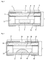
- Fig. 3 is a sectional view taken along a predetermined portion of a condenser microphone manufactured according to the present invention.
- a method for manufacturing a condenser microphone includes: a case 38 serving to protect each part and maintain the outer shape of the condenser microphone and having a sound wave inflow hole 39 formed through the top portion thereof; a filter 41 positioned on the exterior of the case 38, for preventing dust, moisture and foreign materials from flowing into the case 38 through the sound wave inflow hole 39; a diaphragm ring 37 positioned on the interior of the case 38, for maintaining a space in the interior of the case 38 to induce the vibration of sound flowing through the sound wave inflow hole 39; a diaphragm 36 positioned on the bottom end of the diaphragm ring 37 and vibrated by the sound flowing through the sound wave inflow hole 39; a spacer 35 positioned on the bottom end of the diaphragm 36, for maintaining the vibration state of the diaphragm 36 to transmit the vibration of sound; a supporter 33 positioned on the bottom end of the spacer 35, for supporting each part to prevent the movement
- a disc wafer (which is not shown in the drawing) made of silicon single crystal, which is used as a material of a semiconductor integrated circuit (IC), is divided into a plurality of cells.
- the division of the wafer is carried out by using a scribing method where the wafer surface is scribed vertically and horizontally at predetermined intervals by means of a diamond cutter or by using a sawing method where the wafer surface is sawn vertically and horizontally at predetermined intervals by rotating a wheel on which a sharp knife is mounted.
- the sawing method is widely used, since it can provide a relatively smoothly divided surface, thereby ensuring more delicate division.
- each cell of the wafer has a size of 0.4mm x 0.4mm.
- the FET chip 32 is formed on each cell of the wafer.
- the rear surface of the printed circuit board 31 where the circuit of a conductive material is wired re-flows by using a solder paste.
- the solder paste is applied on the portion where soldering is required by the re-flow of the printed circuit board.
- the FET chip 32 formed on the wafer is fixed on a corresponding position of other side of the printed circuit board 31 re-flowing by the application of the solder paste.
- the fixing method is carried out by fixedly bonding the bottom surface of the FET chip 32 onto the corresponding positions of the printed circuit board 31 by means of an adhesive material.
- the adhesive material is made of a semiconductive material obtained by mixing silver (Ag) and an epoxy resin in an appropriate ratio.
- the drain, source and gate of the FET chip 32 and their corresponding positions of the printed circuit board 31 are bonded to each other by using an aluminum wire or a gold wire.
- the bonded portions to the drain and source of the FET chip 32 are connected to the pattern on the bottom surface of the printed circuit board, thereby being connected to external terminals on which the sound signal is outputted.
- connection ring 40 The part of the printed circuit board 31 bonded to the gate terminal of the FET chip 32 comes in contact with the connection ring 40 and becomes conductive, and the connection ring 40 is connected to the back-pole plate 34 and becomes conductive.
- the bonding of the FET chip 32 and the printed circuit board 31 is carried out by means of the aluminum wire or the gold wire, the thickness of the bonding is about 30 ⁇ m, the epoxy resin used is 'CR-2000' or 'CRH-210', and the bonded state is dried for 1.5 hour at a temperature of 150 °C.
- the printed circuit board 31 and the FET chip 32 are potted, i.e. molded by means of the epoxy resin, thereby protecting the product from foreign materials and preventing the erosion of the product.
- a testing step of checking the conductive state that is, the coupled printed circuit board 31 and the FET chip 32 operate normally, is carried out.
- the diaphragm ring 37, the diaphragm 36, the spacer 35, the supporter 33, the back-pole plate 34, the connection ring 40 and the printed circuit board 31 on which the FET chip 32 has been bonded are assembled in the named order within the case 38, thereby producing the condenser microphone.
- the height of the FET chip 32 is 0.2mm and the height of the whole condenser microphone is ranged up to 0.8 ⁇ 1.0 T (mm).
- a method for manufacturing a condenser microphone according to the present invention is capable of providing the following advantages: Firstly, since an FET chip in a wafer state is directly bonded on the pattern on a printed circuit board, the size of the product can be substantially reduced, thereby achieving microminiaturization of the product; the generation of noise caused due to the soldering on the terminals of the FET chip can be prevented; and the occurrence of badness by the disconnection of the terminals bonded on the FET chip due to the heat generated upon soldering can be eliminated.
Landscapes
- Physics & Mathematics (AREA)
- Engineering & Computer Science (AREA)
- Acoustics & Sound (AREA)
- Signal Processing (AREA)
- Electrostatic, Electromagnetic, Magneto- Strictive, And Variable-Resistance Transducers (AREA)
Applications Claiming Priority (2)
| Application Number | Priority Date | Filing Date | Title |
|---|---|---|---|
| KR0027512 | 2000-05-22 | ||
| KR1020000027512A KR100331600B1 (ko) | 2000-05-22 | 2000-05-22 | 콘덴서 마이크로폰의 제조방법 |
Publications (1)
| Publication Number | Publication Date |
|---|---|
| EP1158833A2 true EP1158833A2 (fr) | 2001-11-28 |
Family
ID=19669618
Family Applications (1)
| Application Number | Title | Priority Date | Filing Date |
|---|---|---|---|
| EP00309278A Withdrawn EP1158833A2 (fr) | 2000-05-22 | 2000-10-20 | Procédé de fabrication d'un microphone à condensateur |
Country Status (5)
| Country | Link |
|---|---|
| US (1) | US6323049B1 (fr) |
| EP (1) | EP1158833A2 (fr) |
| JP (1) | JP2001333499A (fr) |
| KR (1) | KR100331600B1 (fr) |
| CN (1) | CN1325259A (fr) |
Cited By (5)
| Publication number | Priority date | Publication date | Assignee | Title |
|---|---|---|---|---|
| EP1513370A3 (fr) * | 2003-09-08 | 2007-08-15 | Sambu Communics Co., Ltd. | Microphone à condensateur |
| EP1696698A3 (fr) * | 2005-02-24 | 2007-08-22 | BSE Co., Ltd. | Microphone à condensateur et procédé pour sa fabrication |
| WO2018032466A1 (fr) | 2016-08-18 | 2018-02-22 | Harman International Industries, Incorporated | Microphone à condensateur électret et procédé de fabrication associé |
| CN108141677A (zh) * | 2015-10-26 | 2018-06-08 | 华为技术有限公司 | 一种扬声器模组、音频补偿方法和装置 |
| TWI712117B (zh) * | 2019-06-20 | 2020-12-01 | 鑫創科技股份有限公司 | 微機電系統麥克風的封裝結構與封裝方法 |
Families Citing this family (11)
| Publication number | Priority date | Publication date | Assignee | Title |
|---|---|---|---|---|
| US7065224B2 (en) | 2001-09-28 | 2006-06-20 | Sonionmicrotronic Nederland B.V. | Microphone for a hearing aid or listening device with improved internal damping and foreign material protection |
| KR20020024122A (ko) * | 2002-01-26 | 2002-03-29 | 이석순 | 콘덴서 마이크로폰 |
| KR100486870B1 (ko) * | 2002-07-30 | 2005-05-03 | 주식회사 비에스이 | 셀프 일렉트렛 콘덴서 마이크로폰 |
| KR100502171B1 (ko) * | 2002-07-30 | 2005-07-22 | 주식회사 비에스이 | 저전압 인가형 콘덴서 마이크로폰 |
| KR100508915B1 (ko) * | 2002-10-10 | 2005-08-19 | 송기영 | 콘덴서 마이크로폰의 구조 및 그 제조 방법 |
| KR20040088753A (ko) * | 2003-04-11 | 2004-10-20 | 주식회사 비에스이 | 정전방전에 대한 내성이 강화된 콘덴서 마이크로폰용전계효과트랜지스터 |
| US7415121B2 (en) | 2004-10-29 | 2008-08-19 | Sonion Nederland B.V. | Microphone with internal damping |
| KR100675024B1 (ko) * | 2005-06-13 | 2007-01-30 | 주식회사 비에스이 | 콘덴서 마이크로폰의 도전 베이스 및 이를 이용한 콘덴서마이크로폰 |
| KR100696166B1 (ko) * | 2005-07-07 | 2007-03-20 | 주식회사 비에스이 | 와이어본딩 인쇄회로기판을 가지는 일렉트릿 콘덴서마이크로폰 및 이의 제조방법 |
| KR100632694B1 (ko) * | 2005-08-20 | 2006-10-16 | 주식회사 비에스이 | 일렉트릿 콘덴서 마이크로폰 |
| CN209283486U (zh) * | 2019-01-10 | 2019-08-20 | 北京搜狗科技发展有限公司 | 一种语音采集设备 |
Family Cites Families (4)
| Publication number | Priority date | Publication date | Assignee | Title |
|---|---|---|---|---|
| JPS5221046Y2 (fr) * | 1971-08-31 | 1977-05-14 | ||
| US4701640A (en) * | 1985-03-11 | 1987-10-20 | Telex Communications, Inc. | Electret transducer and method of fabrication |
| US5097224A (en) * | 1991-04-11 | 1992-03-17 | Telex Communications, Inc. | Self-biasing, low noise amplifier of extended dynamic range |
| US6057175A (en) * | 1997-12-04 | 2000-05-02 | Medtronic, Inc. | Method of making encapsulated package |
-
2000
- 2000-05-22 KR KR1020000027512A patent/KR100331600B1/ko not_active Expired - Fee Related
- 2000-09-20 JP JP2000284451A patent/JP2001333499A/ja active Pending
- 2000-10-03 US US09/679,136 patent/US6323049B1/en not_active Expired - Fee Related
- 2000-10-20 EP EP00309278A patent/EP1158833A2/fr not_active Withdrawn
- 2000-10-20 CN CN00129856A patent/CN1325259A/zh active Pending
Cited By (9)
| Publication number | Priority date | Publication date | Assignee | Title |
|---|---|---|---|---|
| EP1513370A3 (fr) * | 2003-09-08 | 2007-08-15 | Sambu Communics Co., Ltd. | Microphone à condensateur |
| EP1696698A3 (fr) * | 2005-02-24 | 2007-08-22 | BSE Co., Ltd. | Microphone à condensateur et procédé pour sa fabrication |
| CN108141677A (zh) * | 2015-10-26 | 2018-06-08 | 华为技术有限公司 | 一种扬声器模组、音频补偿方法和装置 |
| CN108141677B (zh) * | 2015-10-26 | 2020-02-14 | 华为技术有限公司 | 一种扬声器模组、音频补偿方法和装置 |
| US10667052B2 (en) | 2015-10-26 | 2020-05-26 | Huawei Technologies Co., Ltd. | Speaker module, and audio compensation method and apparatus |
| WO2018032466A1 (fr) | 2016-08-18 | 2018-02-22 | Harman International Industries, Incorporated | Microphone à condensateur électret et procédé de fabrication associé |
| EP3501185A4 (fr) * | 2016-08-18 | 2020-03-18 | Harman International Industries, Incorporated | Microphone à condensateur électret et procédé de fabrication associé |
| US10939192B2 (en) | 2016-08-18 | 2021-03-02 | Harman International Industries, Incorporated | Electret condenser microphone and manufacturing method thereof |
| TWI712117B (zh) * | 2019-06-20 | 2020-12-01 | 鑫創科技股份有限公司 | 微機電系統麥克風的封裝結構與封裝方法 |
Also Published As
| Publication number | Publication date |
|---|---|
| JP2001333499A (ja) | 2001-11-30 |
| KR20010007704A (ko) | 2001-02-05 |
| US6323049B1 (en) | 2001-11-27 |
| KR100331600B1 (ko) | 2002-04-06 |
| CN1325259A (zh) | 2001-12-05 |
Similar Documents
| Publication | Publication Date | Title |
|---|---|---|
| US6323049B1 (en) | Method for manufacturing condenser microphone | |
| US8105856B2 (en) | Method of manufacturing semiconductor device with wiring on side surface thereof | |
| US5606198A (en) | Semiconductor chip with electrodes on side surface | |
| US6258629B1 (en) | Electronic device package and leadframe and method for making the package | |
| US6987312B2 (en) | Semiconductor device with sensor and/or actuator surface and method for producing it | |
| EP1085784A2 (fr) | Dispositif à semiconducteur,microphone capacitif à électret semiconducteur et procédé de production d'un microphone capacitif à électret semiconducteur | |
| JP2001313363A (ja) | 樹脂封止型半導体装置 | |
| JP2001196488A (ja) | 電子部品装置及びその製造方法 | |
| KR100380701B1 (ko) | 표면장착용반도체장치제조방법및표면장착용반도체장치 | |
| EP1478021B1 (fr) | Dispositif semiconducteur et son procédé de fabrication | |
| US6683370B1 (en) | Semiconductor component and method of manufacturing same | |
| KR20050039650A (ko) | 압전 발진기와 전자 기기 및 압전 발진기의 제조방법 | |
| KR20010074030A (ko) | 콘덴서 마이크로폰의 제조방법 | |
| JPH06244304A (ja) | リードレスチップキャリアパッケージ | |
| KR100411619B1 (ko) | 콘덴서 마이크로폰의 구조 및 그 제조 방법 | |
| US20020135050A1 (en) | Semiconductor device | |
| EP0893861A2 (fr) | Module optique | |
| JP2533012B2 (ja) | 表面実装型半導体装置 | |
| KR100375168B1 (ko) | 반도체 패키지 및 그 제조방법 | |
| US12584740B2 (en) | Electronic component, sensor module, and method for manufacturing electronic component | |
| KR20020050556A (ko) | 반도체 리드프레임과 이를 채용한 반도체 패키지 | |
| KR100643911B1 (ko) | 초소형 콘덴서 마이크로폰 및 그 제조방법 | |
| JP2568057B2 (ja) | 集積回路装置 | |
| JP3586867B2 (ja) | 半導体装置、その製造方法及びその実装方法並びにこれを実装した回路基板 | |
| JPH08125154A (ja) | 半導体装置の製造方法 |
Legal Events
| Date | Code | Title | Description |
|---|---|---|---|
| PUAI | Public reference made under article 153(3) epc to a published international application that has entered the european phase |
Free format text: ORIGINAL CODE: 0009012 |
|
| AK | Designated contracting states |
Kind code of ref document: A2 Designated state(s): AT BE CH CY DE DK ES FI FR GB GR IE IT LI LU MC NL PT SE |
|
| AX | Request for extension of the european patent |
Free format text: AL;LT;LV;MK;RO;SI |
|
| STAA | Information on the status of an ep patent application or granted ep patent |
Free format text: STATUS: THE APPLICATION IS DEEMED TO BE WITHDRAWN |
|
| 18D | Application deemed to be withdrawn |
Effective date: 20030503 |