EP1160724A2 - Kontaktanordnung für mehrkomponentige Smart Cards - Google Patents
Kontaktanordnung für mehrkomponentige Smart Cards Download PDFInfo
- Publication number
- EP1160724A2 EP1160724A2 EP01110958A EP01110958A EP1160724A2 EP 1160724 A2 EP1160724 A2 EP 1160724A2 EP 01110958 A EP01110958 A EP 01110958A EP 01110958 A EP01110958 A EP 01110958A EP 1160724 A2 EP1160724 A2 EP 1160724A2
- Authority
- EP
- European Patent Office
- Prior art keywords
- contact
- bumps
- arrangement according
- card
- card body
- Prior art date
- Legal status (The legal status is an assumption and is not a legal conclusion. Google has not performed a legal analysis and makes no representation as to the accuracy of the status listed.)
- Withdrawn
Links
Images
Classifications
-
- G—PHYSICS
- G06—COMPUTING OR CALCULATING; COUNTING
- G06K—GRAPHICAL DATA READING; PRESENTATION OF DATA; RECORD CARRIERS; HANDLING RECORD CARRIERS
- G06K19/00—Record carriers for use with machines and with at least a part designed to carry digital markings
- G06K19/06—Record carriers for use with machines and with at least a part designed to carry digital markings characterised by the kind of the digital marking, e.g. shape, nature, code
- G06K19/067—Record carriers with conductive marks, printed circuits or semiconductor circuit elements, e.g. credit or identity cards also with resonating or responding marks without active components
- G06K19/07—Record carriers with conductive marks, printed circuits or semiconductor circuit elements, e.g. credit or identity cards also with resonating or responding marks without active components with integrated circuit chips
- G06K19/077—Constructional details, e.g. mounting of circuits in the carrier
- G06K19/07743—External electrical contacts
Definitions
- the invention relates to a contact arrangement for multi-component smart cards, which connect the card body in one or more planes, the electrical and / or electronic components of the smart card interconnect interconnects and to form contact areas for external contacting of the card for the purpose of data exchange with serves a host system.
- the document discloses a technology for contacting of the microchip on a contact unit with the connection points on the chip as elevations made of an electrically conductive material in the form of a conductive adhesive, a meltable alloy or a solder paste are.
- the use of bumps to create contact points is also already in connection with the contacting of so-called surface-mounted Components (SMD - Surface Mounted Devices) on printed circuit boards or known on carriers of hybrid components.
- SMD Surface-mounted Components
- peripheral components working with the chip such as for example displays, batteries or other optical or electrical / electronic Integrate elements into the map.
- peripheral components working with the chip such as for example displays, batteries or other optical or electrical / electronic Integrate elements into the map.
- the function and interaction of the components is their internal interconnection required.
- Conductor tracks which in turn determined the circuit technology for this purpose Make with each other and with the contacts used for external contacting in Have to be connected.
- the object of the present invention is to create a contact arrangement, what contact areas for external contacting a smart card with a Host system trains while connecting to the card body arranged conductor tracks with each other as well as with the external contacts guaranteed.
- the construction should be simple in terms of production technology Contact arrangement a high-precision connection of the preferably self-adjusting Contacts may be possible.
- the proposed contact arrangement for solving the task consists of a a recess in the card body introduced contact unit, galvanic Contact areas on the conductor tracks running in the card body as well as contacting elements, which the contact unit and the contact surfaces electrically connect with each other.
- the one with a metallization layer Carrier-formed contact unit points in a known manner for external contacting the smart card by structuring its metallization layer accordingly several ISO contacts on the surface facing away from the card body.
- On the back of the card body facing one or more of these ISO contacts are the contacting elements for connecting the contact unit with the conductor tracks in the form of bumps.
- the Bumps are attached to the contact surfaces below the ISO contacts Contact unit contacted conductor tracks contacted.
- the one used to construct the contact arrangement Contact unit optionally as pure, the electrical connection of the conductor tracks mutual and external contact or at the same time as Component carrier for a flip-chip technology on the back of your Used ISO contacts contacted card chip.
- a possible embodiment of the contact arrangement according to the invention is thereby given that the bumps on the back of the card body facing the Contact unit usually existing contact pads are applied. As well the bumps can also be arranged instead of the contact pads. Corresponding An advantageous embodiment of the invention is between the contact pads and arranged a diffusion barrier to the bumps. Here comes as a diffusion barrier preferably a Ni / Au layer is used.
- bumps on the back of the ISO contacts Possibilities.
- One way is to find the appropriate one Apply elevations galvanically. But it is also possible to do the bumps in the form of a material application applied by means of screen printing.
- a Another option is to use solder balls, so-called spheres, to bump the to be realized, which by melting with the back of the ISO contacts or the contact pads available there are connected.
- the bumps have no major technological Difficulty connecting to the pads the conductor tracks in the card body can be adjusted to the required height.
- the height of the bumps can be continuous as they melt between 50 ⁇ m and the maximum height of the card.
- the connection the bumps with the contact surfaces of the conductor tracks can be made using various Technologies. To make the connection comes a glue isotropic or anisotropic adhesives, melting (soldering) or bonding (Ultrasonic welding) of the bumps.
- the invention allows the advantages of the in a particularly advantageous manner Flip-chip technology as currently the fastest, cheapest and most reliable connection technology between chip and contact unit of a card with the requirements an interconnection of additional components to a smart card Unite chip card.
- the invention combines the connection technology according to the flip-chip technology with the contact surface standardized according to ISO-7810 for Smart cards.
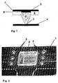
- A is shown Part that is used for external contacting and, if necessary, for connection to a Microchip 9 provided contact unit 1, which is provided with a metallization layer 7 provided carrier 6 is formed.
- a metallization layer 7 provided carrier 6 is formed.
- it is included on an epoxy carrier to form the ISO contacts 5 for external contacting an Au / Ni layer is applied.
- On the side of the card body facing the Contact unit 1 are provided in the carrier 6 contact window 10.
- a diffusion barrier 8 is arranged between the rear contact surface of the ISO contacts 5 and the bumps 2 is in In the form of a Ni / Au layer.
- the bumps 2 are set to the required height.
- the Bumps 2 are designed so that they are set in a height range of 50 ⁇ m and the maximum card height is possible.
- solder balls in precisely defined volumes up to diameters of 50 microns are produced, so that due to the surface tension after the Melt a self-adjustment at the contact point with the contact unit 1 takes place and at the same time a precisely defined height profile is set.
- FIG. 2 shows a good impression of the structure of the implementation given the contact arrangement according to the invention serving contact unit 1.
- the figure relates to a top view of the assembly of the contact unit 1 surface of the unit 1 facing the card body.
- the contact unit 1 serves the contact unit 1 except for the formation of the ISO contacts 5 and the connection the interconnects 4 arranged inside the card body or with the ISO contacts 5 at the same time as a component carrier for the after Flip chip technology card chip 9 connected to the carrier.
- the solder bumps arranged on the back of the ISO contacts 5.
- the metallization area 7 of the contact unit is used to form the usual 6 to 8 contacts for external contacting by appropriate interruptions 11 in the metallization area 7 structured.
- the structuring on the top of the card trained ISO contacts 5 can by the invention on the bumps 2 any layers of the card body can be contacted. Remarkably thereby that the previously known structure of the contact unit carrying the chip in Essentially, it can be maintained so that, apart from that for Connection of the bumps 2 with the contact unit 1 and the contact surfaces 3 on the Conductors 4 connection technology to be used, no essential Changes in process technology are required.
Landscapes
- Engineering & Computer Science (AREA)
- Computer Hardware Design (AREA)
- Microelectronics & Electronic Packaging (AREA)
- Physics & Mathematics (AREA)
- General Physics & Mathematics (AREA)
- Theoretical Computer Science (AREA)
- Credit Cards Or The Like (AREA)
Abstract
Description
- Fig.1:
- Eine ausschnittweise Darstellung der erfindungsgemäßen Kontaktanordnung;
- Fig. 2:
- Eine Kontakteinheit mit Lotbumps und an der Kontakteinheit kontaktiertem Chip.
- 1
- Kontakteinheit
- 2
- Kontaktelement, Bump
- 3
- Kontaktfläche
- 4
- Leiterbahn
- 5
- ISO-Kontakt
- 6
- Träger
- 7
- Metallisierungsschicht
- 8
- Diffusionssperre
- 9
- Mikrochip
- 10
- Kontaktfenster
- 11
- Unterbrechungen
Claims (12)
- Kontaktanordnung für mehrkomponentige Smart Cards, zur Verbindung von in einer oder mehreren Ebenen in den Kartenkörper eingeordneten, die darin integrierten elektrischen und/oder elektronischen Komponenten der Smart Card untereinander verschaltenden Leiterbahnen (4) und zur Bildung von Kontaktflächen (5) für eine externe Kontaktierung der Karte zum Datenaustausch mit einem Hostsystem, bestehend aus einer in eine Aussparrung des Kartenkörpers eingebrachten Kontakteinheit (1), galvanischen Kontaktflächen (3) auf den Leiterbahnen (4) sowie die Kontakteinheit (1) und die Kontaktflächen (3) elektrisch miteinander verbindenden Kontaktierungselementen (2), wobei die Kontakteinheit (1), welche aus einem mit einer Metalisierungsschicht (7) versehenem Träger (6) gebildet ist, zur externen Kontaktierung der Smart Card durch eine entsprechende Strukturierung ihrer Metalisierungsschicht (7) auf der dem Kartenkörper abgewandten Oberfläche mehrere ISO-Kontakte (5) aufweist und die Kontaktierungselemente (2) als auf der dem Kartenkörper zugewandten Rückseite eines oder mehrerer dieser ISO-Kontakte (5) aufgebrachte Erhöhungen (Bumps) ausgebildet und mit den Kontaktflächen (3) der unterhalb der ISO-Kontakte (5) an die Kontakteinheit (1) herangeführten Leiterbahnen (4) kontaktiert sind .
- Kontaktanordnung nach Anspruch 1, dadurch gekennzeichnet, dass die Kontakteinheit (1) gleichzeitig als Bauelementeträger für einen nach der Flip-Chip-Technologie an der Rückseite ihrer ISO-Kontakte (5) kontaktierten Kartenchip (9) dient.
- Kontaktanordnung nach Anspruch 1 oder 2, dadurch gekennzeichnet, dass die Bumps (2) auf an der dem Kartenkörper zugewandten Rückseite der Kontakteinheit (1) vorhandene Kontaktpads aufgebracht sind.
- Kontaktanordnung nach einem Ansprüche 1 bis 3, dadurch gekennzeichnet, dass zwischen der rückseitigen Kontaktierungsfläche der ISO-Kontakte und den Bumps (2) eine Diffusionssperre (8) eingeordnet ist.
- Kontaktanordnung nach Anspruch 4, dadurch gekennzeichnet, dass es sich bei der Diffusionssperre (8) um eine Ni/Au-Schicht handelt.
- Kontaktanordnung nach einem der Ansprüche 1 bis 5, dadurch gekennzeichnet, dass die Bumps (2) als galvanisch aufgebrachte Erhöhungen ausgebildet sind.
- Kontaktanordnung nach einem der Ansprüche 1 bis 5, dadurch gekennzeichnet, dass die Bumps (2) als mittels Siebdruck aufgebrachte Erhöhungen ausgebildet sind.
- Kontaktanordnung nach einem der Ansprüche 1 bis 5, dadurch gekennzeichnet, dass die Bumps (2) als in Form von Lotkugeln (Spheres) aufgebrachte Lotkugeln ausgebildet sind.
- Kontaktanordnung nach einem der Ansprüche 1 bis 8, dadurch gekennzeichnet, dass die Höhe der Bumps (2) entsprechend der Tiefe der mit ihnen zur Verbindung vorgesehenen Leiterbahn (4) im Kartenkörper durch Aufschmelzen zwischen 50 µm und der Maximalhöhe der Karte einstellbar ist.
- Kontaktanordnung nach einem der Ansprüche 1 bis 9, dadurch gekennzeichnet, dass die Bumps (2) mit der Kontaktfläche (3) des zugehörigen Gegenkontaktes einer Leiterbahn (4) verklebt sind.
- Kontaktanordnung nach einem der Ansprüche 1 bis 9, dadurch gekennzeichnet, dass die Bumps (2) mit der Kontaktfläche (3) des zugehörigen Gegenkontaktes einer Leiterbahn (4) durch Aufschmelzen verlötet sind.
- Kontaktanordnung nach einem der Ansprüche 1 bis 9, dadurch gekennzeichnet, dass die Bumps (2) auf die Kontaktfläche (3) des zugehörigen Gegenkontaktes einer Leiterbahn (4) durch Ultraschallschweißen gebondet sind.
Applications Claiming Priority (2)
| Application Number | Priority Date | Filing Date | Title |
|---|---|---|---|
| DE2000125147 DE10025147C2 (de) | 2000-05-20 | 2000-05-20 | Kontaktanordnung für mehrkomponentige Smart Cards |
| DE10025147 | 2000-05-20 |
Publications (2)
| Publication Number | Publication Date |
|---|---|
| EP1160724A2 true EP1160724A2 (de) | 2001-12-05 |
| EP1160724A3 EP1160724A3 (de) | 2003-03-26 |
Family
ID=7643022
Family Applications (1)
| Application Number | Title | Priority Date | Filing Date |
|---|---|---|---|
| EP01110958A Withdrawn EP1160724A3 (de) | 2000-05-20 | 2001-05-07 | Kontaktanordnung für mehrkomponentige Smart Cards |
Country Status (2)
| Country | Link |
|---|---|
| EP (1) | EP1160724A3 (de) |
| DE (1) | DE10025147C2 (de) |
Families Citing this family (1)
| Publication number | Priority date | Publication date | Assignee | Title |
|---|---|---|---|---|
| DE102004010715B4 (de) * | 2004-03-04 | 2009-10-01 | Infineon Technologies Ag | Chipkarte zur kontaktlosen Datenübertragung sowie Verfahren zum Herstellen einer Chipkarte zur kontaktlosen Datenübertragung |
Citations (1)
| Publication number | Priority date | Publication date | Assignee | Title |
|---|---|---|---|---|
| US5598032A (en) * | 1994-02-14 | 1997-01-28 | Gemplus Card International | Hybrid chip card capable of both contact and contact-free operation and having antenna contacts situated in a cavity for an electronic module |
Family Cites Families (7)
| Publication number | Priority date | Publication date | Assignee | Title |
|---|---|---|---|---|
| DE4325458A1 (de) * | 1993-07-29 | 1995-02-09 | Orga Bond Technik Gmbh | Trägerelement für einen IC-Baustein |
| DE4442960C1 (de) * | 1994-12-02 | 1995-12-21 | Fraunhofer Ges Forschung | Lothöcker für die Flip-Chip-Montage und Verfahren zu dessen Herstellung |
| DE4443980C2 (de) * | 1994-12-11 | 1997-07-17 | Angewandte Digital Elektronik | Verfahren zur Herstellung von Chipkarten und Chipkarte hergestellt nach diesem Verfahren |
| DE19500925C2 (de) * | 1995-01-16 | 1999-04-08 | Orga Kartensysteme Gmbh | Verfahren zur Herstellung einer kontaktlosen Chipkarte |
| DE19612718B4 (de) * | 1996-03-29 | 2006-06-29 | Ods Landis & Gyr Gmbh & Co. Kg | Chipkarte mit Batterie sowie Verfahren zur Montage einer Chipmodul/Batterie-Einheit |
| DE19738399A1 (de) * | 1997-09-03 | 1999-03-04 | Bosch Gmbh Robert | Verfahren zur Verbindung von elektronischen Bauelementen mit einem Trägersubstrat |
| DE19933757A1 (de) * | 1999-07-19 | 2001-01-25 | Giesecke & Devrient Gmbh | Chipkarte mit integrierter Batterie |
-
2000
- 2000-05-20 DE DE2000125147 patent/DE10025147C2/de not_active Expired - Fee Related
-
2001
- 2001-05-07 EP EP01110958A patent/EP1160724A3/de not_active Withdrawn
Patent Citations (1)
| Publication number | Priority date | Publication date | Assignee | Title |
|---|---|---|---|---|
| US5598032A (en) * | 1994-02-14 | 1997-01-28 | Gemplus Card International | Hybrid chip card capable of both contact and contact-free operation and having antenna contacts situated in a cavity for an electronic module |
Also Published As
| Publication number | Publication date |
|---|---|
| EP1160724A3 (de) | 2003-03-26 |
| DE10025147C2 (de) | 2002-03-07 |
| DE10025147A1 (de) | 2001-11-22 |
Similar Documents
| Publication | Publication Date | Title |
|---|---|---|
| DE19534480C2 (de) | IC-Kartenmodul zur Herstellung einer IC-Karte sowie IC-Karte mit einem IC-Kartenmodul | |
| DE19708617C2 (de) | Chipkartenmodul und Verfahren zu seiner Herstellung sowie diesen umfassende Chipkarte | |
| DE19500925A1 (de) | Chipkarte zur kontaktlosen Datenübertragung | |
| EP1152368A1 (de) | Chipkarte | |
| WO1999005647A1 (de) | Kontaktlos betreibbarer datenträger | |
| DE19929610C1 (de) | Chipmodul, Chipkarte und Verfahren zu deren Herstellung | |
| EP4404101A2 (de) | Kartenförmiger datenträger sowie halbzeug und kontaktlayout dafür, und verfahren zur herstellung derselben | |
| DE19920444B4 (de) | Verfahren zum Herstellen eines Halbleiterbausteins sowie Halbleiterbaustein | |
| EP3066618B1 (de) | Ic-modul für unterschiedliche verbindungstechniken | |
| DE19716342C2 (de) | Verfahren zur Herstellung einer Chipkarte | |
| DE10141571B4 (de) | Verfahren zum Zusammenbau eines Halbleiterbauelements und damit hergestellte integrierte Schaltungsanordnung, die für dreidimensionale, mehrschichtige Schaltungen geeignet ist | |
| EP0818752A2 (de) | Leiterplatte (Inlet) für Chip-Karten | |
| DE102007022615A1 (de) | Kontaktloses Übertragungssystem und Verfahren zum Herstellen desselben | |
| DE10025147C2 (de) | Kontaktanordnung für mehrkomponentige Smart Cards | |
| EP0995235B1 (de) | Kontakt für kleinste bondkontakte sowie verfahren zur herstellung eines kontaktes | |
| DE102020122437A1 (de) | Package, Verfahren zum Bilden eines Packages, Trägerband, Chipkarte und Verfahren zum Bilden eines Trägerbands | |
| EP1247250B1 (de) | Chipkartenanordnung | |
| DE10210608C1 (de) | Tragbarer Datenträger mit Display und Verfahren zu seiner Herstellung | |
| EP1536372B1 (de) | Verfahren zur Herstellung von Datenträgern und nach diesem Verfahren hergestellter Datenträger | |
| DE102004055616B4 (de) | Verfahren zum Verbinden einer Modulbrücke mit einem Substrat und mehrschichtiger Transponder | |
| DE19647845C2 (de) | Verfahren zum Herstellen einer Chipkarte | |
| DE29801806U1 (de) | Taschen- oder Armbanduhr mit Chipkartenfunktion | |
| DE102022109547A1 (de) | Kartenförmiger Datenträger sowie Halbzeug und Kontaktlayout dafür, und Verfahren zur Herstellung derselben | |
| EP1684216A1 (de) | Tragbarer Datenträger | |
| DE19637215A1 (de) | Verfahren und Verbindungsanordnung zum Herstellen einer Chipkarte |
Legal Events
| Date | Code | Title | Description |
|---|---|---|---|
| PUAI | Public reference made under article 153(3) epc to a published international application that has entered the european phase |
Free format text: ORIGINAL CODE: 0009012 |
|
| AK | Designated contracting states |
Kind code of ref document: A2 Designated state(s): AT BE CH CY DE DK ES FI FR GB GR IE IT LI LU MC NL PT SE TR |
|
| AX | Request for extension of the european patent |
Free format text: AL;LT;LV;MK;RO;SI |
|
| PUAL | Search report despatched |
Free format text: ORIGINAL CODE: 0009013 |
|
| AK | Designated contracting states |
Kind code of ref document: A3 Designated state(s): AT BE CH CY DE DK ES FI FR GB GR IE IT LI LU MC NL PT SE TR Designated state(s): AT BE CH CY DE DK ES FI FR GB GR IE IT LI LU MC NL PT SE TR |
|
| AX | Request for extension of the european patent |
Extension state: AL LT LV MK RO SI |
|
| RIC1 | Information provided on ipc code assigned before grant |
Ipc: 7H 05K 3/34 B Ipc: 7H 01L 23/485 B Ipc: 7G 06K 19/077 B Ipc: 7G 06K 19/067 A |
|
| 17P | Request for examination filed |
Effective date: 20030219 |
|
| 17Q | First examination report despatched |
Effective date: 20030430 |
|
| AKX | Designation fees paid |
Designated state(s): AT BE CH CY DE DK ES FI FR GB GR IE IT LI LU MC NL PT SE TR |
|
| STAA | Information on the status of an ep patent application or granted ep patent |
Free format text: STATUS: THE APPLICATION IS DEEMED TO BE WITHDRAWN |
|
| 18D | Application deemed to be withdrawn |
Effective date: 20040817 |