EP1160845A2 - Verfahren zur Herstellung von einem Halbleiterbauelement aus Siliziumkarbid - Google Patents
Verfahren zur Herstellung von einem Halbleiterbauelement aus Siliziumkarbid Download PDFInfo
- Publication number
- EP1160845A2 EP1160845A2 EP01112273A EP01112273A EP1160845A2 EP 1160845 A2 EP1160845 A2 EP 1160845A2 EP 01112273 A EP01112273 A EP 01112273A EP 01112273 A EP01112273 A EP 01112273A EP 1160845 A2 EP1160845 A2 EP 1160845A2
- Authority
- EP
- European Patent Office
- Prior art keywords
- substrate
- sic substrate
- semiconductor layer
- doped layer
- dopant
- Prior art date
- Legal status (The legal status is an assumption and is not a legal conclusion. Google has not performed a legal analysis and makes no representation as to the accuracy of the status listed.)
- Ceased
Links
Images




Classifications
-
- H—ELECTRICITY
- H10—SEMICONDUCTOR DEVICES; ELECTRIC SOLID-STATE DEVICES NOT OTHERWISE PROVIDED FOR
- H10D—INORGANIC ELECTRIC SEMICONDUCTOR DEVICES
- H10D8/00—Diodes
- H10D8/01—Manufacture or treatment
- H10D8/051—Manufacture or treatment of Schottky diodes
-
- H—ELECTRICITY
- H10—SEMICONDUCTOR DEVICES; ELECTRIC SOLID-STATE DEVICES NOT OTHERWISE PROVIDED FOR
- H10D—INORGANIC ELECTRIC SEMICONDUCTOR DEVICES
- H10D12/00—Bipolar devices controlled by the field effect, e.g. insulated-gate bipolar transistors [IGBT]
- H10D12/01—Manufacture or treatment
- H10D12/031—Manufacture or treatment of IGBTs
-
- H—ELECTRICITY
- H10—SEMICONDUCTOR DEVICES; ELECTRIC SOLID-STATE DEVICES NOT OTHERWISE PROVIDED FOR
- H10D—INORGANIC ELECTRIC SEMICONDUCTOR DEVICES
- H10D62/00—Semiconductor bodies, or regions thereof, of devices having potential barriers
- H10D62/80—Semiconductor bodies, or regions thereof, of devices having potential barriers characterised by the materials
- H10D62/83—Semiconductor bodies, or regions thereof, of devices having potential barriers characterised by the materials being Group IV materials, e.g. B-doped Si or undoped Ge
- H10D62/832—Semiconductor bodies, or regions thereof, of devices having potential barriers characterised by the materials being Group IV materials, e.g. B-doped Si or undoped Ge being Group IV materials comprising two or more elements, e.g. SiGe
- H10D62/8325—Silicon carbide
-
- H—ELECTRICITY
- H10—SEMICONDUCTOR DEVICES; ELECTRIC SOLID-STATE DEVICES NOT OTHERWISE PROVIDED FOR
- H10P—GENERIC PROCESSES OR APPARATUS FOR THE MANUFACTURE OR TREATMENT OF DEVICES COVERED BY CLASS H10
- H10P30/00—Ion implantation into wafers, substrates or parts of devices
- H10P30/20—Ion implantation into wafers, substrates or parts of devices into semiconductor materials, e.g. for doping
- H10P30/202—Ion implantation into wafers, substrates or parts of devices into semiconductor materials, e.g. for doping characterised by the semiconductor materials
- H10P30/204—Ion implantation into wafers, substrates or parts of devices into semiconductor materials, e.g. for doping characterised by the semiconductor materials into Group IV semiconductors
- H10P30/2042—Ion implantation into wafers, substrates or parts of devices into semiconductor materials, e.g. for doping characterised by the semiconductor materials into Group IV semiconductors into crystalline silicon carbide
-
- H—ELECTRICITY
- H10—SEMICONDUCTOR DEVICES; ELECTRIC SOLID-STATE DEVICES NOT OTHERWISE PROVIDED FOR
- H10P—GENERIC PROCESSES OR APPARATUS FOR THE MANUFACTURE OR TREATMENT OF DEVICES COVERED BY CLASS H10
- H10P30/00—Ion implantation into wafers, substrates or parts of devices
- H10P30/20—Ion implantation into wafers, substrates or parts of devices into semiconductor materials, e.g. for doping
- H10P30/21—Ion implantation into wafers, substrates or parts of devices into semiconductor materials, e.g. for doping of electrically active species
-
- H—ELECTRICITY
- H10—SEMICONDUCTOR DEVICES; ELECTRIC SOLID-STATE DEVICES NOT OTHERWISE PROVIDED FOR
- H10P—GENERIC PROCESSES OR APPARATUS FOR THE MANUFACTURE OR TREATMENT OF DEVICES COVERED BY CLASS H10
- H10P30/00—Ion implantation into wafers, substrates or parts of devices
- H10P30/20—Ion implantation into wafers, substrates or parts of devices into semiconductor materials, e.g. for doping
- H10P30/28—Ion implantation into wafers, substrates or parts of devices into semiconductor materials, e.g. for doping characterised by an annealing step, e.g. for activation of dopants
-
- H—ELECTRICITY
- H10—SEMICONDUCTOR DEVICES; ELECTRIC SOLID-STATE DEVICES NOT OTHERWISE PROVIDED FOR
- H10P—GENERIC PROCESSES OR APPARATUS FOR THE MANUFACTURE OR TREATMENT OF DEVICES COVERED BY CLASS H10
- H10P50/00—Etching of wafers, substrates or parts of devices
-
- H—ELECTRICITY
- H10—SEMICONDUCTOR DEVICES; ELECTRIC SOLID-STATE DEVICES NOT OTHERWISE PROVIDED FOR
- H10D—INORGANIC ELECTRIC SEMICONDUCTOR DEVICES
- H10D10/00—Bipolar junction transistors [BJT]
- H10D10/01—Manufacture or treatment
- H10D10/021—Manufacture or treatment of heterojunction BJTs [HBT]
Definitions
- the present invention relates to a semiconductor device fabrication process that includes the process step of implanting dopant ions into a semiconductor layer containing Si and C, e.g., an SiC or SiGeC layer.
- SiC Silicon carbide
- SiC is a semiconductor that has a wider bandgap than that of silicon (Si). Accordingly, SiC has a higher breakdown field and a higher melting point compared to Si. In view of these beneficial properties, SiC is a semiconductor material hopefully applicable to next-generation power electronic devices, RF devices, high-temperature-operating devices and so on. It is also known that Sic can take various crystal structures including cubic ones such as 3C-SiC and hexagonal ones like 6H-SiC and 4H-SiC.
- an SiC device is formed by defining some required regions in an SiC substrate.
- a diode for example, p-, i- (intrinsic) and n-type regions need to be defined in an SiC substrate.
- source/drain and channel regions should be defined therein.
- any particular region of the SiC substrate can have a desired conductivity type by implanting ions of a dopant into the substrate. More specifically, where an n-type region should be defined, ions of an n-type dopant, like nitrogen (N), phosphorus (P), etc., may be implanted into the substrate.
- N nitrogen
- P phosphorus
- a p-type region may be defined by implanting ions of a p-type dopant, e.g., boron (B), aluminum (Al), etc., into the substrate.
- a p-type dopant e.g., boron (B), aluminum (Al), etc.
- the SiC substrate, into which the dopant ions have been implanted is placed in an annealing furnace and then heated to an elevated temperature of 1300°C or more with argon gas supplied into the furnace at the atmospheric pressure.
- the ion-implanted regions in the SiC substrate can have their crystallinity recovered (or their damage repaired) and the dopant atoms introduced can be activated at a time.
- FIG. 8 illustrates a vertical dopant (Al in this case) concentration profile in an SiC substrate that has been subjected to the known ion implantation process.
- the ions, which have been implanted into the SiC substrate have hardly diffused even after the substrate has been annealed at 1300°C or more. Accordingly, even after the substrate has been annealed, the profile of the dopant, introduced into the substrate by performing the ion implantation process only once, still shows a Gaussian distribution just like before the dopant introduced is annealed.
- the ion implantation process is normally performed several times with the implant energy changed each time, thereby trying to define a doped region with as uniform a concentration as possible and with a predetermined width.
- the dopant concentration is unexpectedly low in the upper part of the SiC substrate over the uppermost dopant concentration peak located at a depth of about 1000 nm. That is to say, a region with a non-controllable dopant concentration exists in that part of the SiC substrate over the depth of about 1000 nm.
- That upper part of the SiC substrate which is a relatively thick region located over the uppermost peak of dopant concentration and has the unexpectedly low dopant concentration, may be removed.
- the current process technology for MOS transistors and so on to be formed on an Si substrate is applicable for this purpose in the following manner. Specifically, after the SiC substrate has been annealed, part of the substrate, usually hard to wet-etch away directly, can be removed either by performing a dry etching process using a plasma or by thermally oxidizing that part of the substrate and then wet-etching the oxide film away.
- the plasma to be produced should have a rather high energy. Accordingly, when the surface of the SiC substrate is exposed to such high-energy radiation, defects might be newly created in the upper part of the SiC substrate again. Thus, it is expected that even if the substrate is annealed again after that, it will be still difficult to recover the crystallinity sufficiently. On the other hand, according to the latter thermal oxide forming/removing technique, it takes a great deal of time and trouble.
- the thickness of an oxide film that can be formed by a single thermal oxidation process is at most about 100 nm, due to the low oxidation rate, and the thermal oxidation and wet etching should be performed as many as ten times just to remove that part.
- An inventive method is applicable to fabricating a semiconductor device on a substrate, which includes a semiconductor layer containing at least silicon and carbon, so that an active region of the device is defined in the semiconductor layer.
- the method includes the step of a) implanting ions of a dopant into the semiconductor layer.
- the method further includes the step of b) placing the substrate in a chamber and removing part of the semiconductor layer to a predetermined depth with the substrate heated at least to a temperature at which the dopant is activated. The depth is measured from the surface of the semiconductor layer.
- the step b) is performed after the step a) has been performed.
- the profile of a dopant, which has been introduced into the layer through ion implantation hardly changes even after the substrate has been subjected to an annealing process to activate the dopant. Even so, according to the present invention, any peak of the dopant concentration in the surface region of the semiconductor layer can be located at the surface by removing the part over the peak. In addition, the surface region, which has been damaged particularly seriously through the ion implantation processes, can be removed. Accordingly, when an electrode that makes a Schottky or ohmic contact with the semiconductor layer should be formed on the layer, desired characteristics are easily realizable.
- that part of the semiconductor layer may be removed in the step b) so that the dopant has a predetermined concentration at the surface of the other remaining part of the semiconductor layer. Then, a Schottky or ohmic electrode with desired characteristics can be formed accurately.
- an etching gas which has a property of etching the semiconductor layer, may be introduced into the chamber in the step b) to etch away said part of the semiconductor layer. In this manner, the surface part of the semiconductor layer is removable without doing any additional damage on the remaining part of the semiconductor layer.
- the semiconductor layer may be made of silicon carbide.
- that part of the semiconductor layer may be etched away using a gas that contains at least one element selected from the group consisting of hydrogen and the halogen elements.
- the substrate is preferably heated in the step b) to a temperature between 1300°C and 2300°C. Then, the implant-induced damage in the semiconductor layer can be repaired while the upper part thereof is being removed.
- the etching gas is preferably supplied in the step b) at a flow rate between 0.001 l/min and 10 l/min.
- the first embodiment represents the basic idea of the inventive concurrent anneal-etch process.
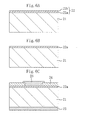
- FIGS. 1A through 1C illustrate fundamental process steps for forming an SiC layer for a semiconductor device in accordance with the present invention.
- an SiC substrate 11 is prepared.
- the substrate 11 may be a 6H-SiC substrate with a (0001) off-axis plane as its principal surface. That is to say, the principal surface of the SiC substrate 11 may tilt from a (0001) crystallographic plane (i.e., a C-plane) in the [11-20] direction by 3.5 degrees.
- the surface of the 6H-SiC substrate 11 may be an n-type Si face in which Si atoms are closely packed.
- the SiC substrate 11 may have a diameter of be about 25 mm, for example.
- Al ions Al +
- Al ions Al +
- a p-type doped layer 12 into which Al atoms have been introduced, is formed in the SiC substrate 11.
- part of the doped layer 12, located under the uppermost peak Prp7 may be a lower doped layer 12a, while the other part thereof located over the uppermost peak Prp7 may be an upper doped layer 12b.
- the boundary between the upper and lower doped layers 12b and 12a does not have to correspond to the uppermost peak Prp7. So in this and following embodiments, the upper doped layer 12b shall mean part of the doped layer 12 to be etched away, while the lower doped layer 12a the other part thereof to be left.
- the ion implantation processes are performed under the following conditions. Specifically, the first ion implantation process, corresponding to the peak Prp1, is performed at an accelerating voltage of 7.0 MeV and at a dose of 3 ⁇ 10 14 atoms ⁇ cm -2 .
- the second ion implantation process, corresponding to the peak Prp2 is performed at an accelerating voltage of 5.6 MeV and at a dose of 3 ⁇ 10 14 atoms ⁇ cm -2 .
- the third ion implantation process, corresponding to the peak Prp3 is performed at an accelerating voltage of 4.4 MeV and at a dose of 7 ⁇ 10 14 atoms ⁇ cm -2 .
- the fourth ion implantation process corresponding to the peak Prp4, is performed at an accelerating voltage of 3.3 MeV and at a dose of 7 ⁇ 10 14 atoms ⁇ cm -2 .
- the fifth ion implantation process, corresponding to the peak Prp5 is performed at an accelerating voltage of 2.4 MeV and at a dose of 3 ⁇ 10 14 atoms ⁇ cm -2 .
- the sixth ion implantation process, corresponding to the peak Prp6, is performed at an accelerating voltage of 1.6 MeV and at a dose of 3 ⁇ 10 14 atoms ⁇ cm -2 .
- the seventh ion implantation process corresponding to the peak Prp7, is performed at an accelerating voltage of 1.0 MeV and at a dose of 3 ⁇ 10 14 atoms ⁇ cm -2 .
- the direction in which the Al ions are implanted may form an angle of seven degrees with a normal to the surface of the SiC substrate 11.
- These ion implantation processes are always performed at room temperature.
- the Al concentration profile in the doped layer formed by these ion implantation processes was measured using a secondary ion mass spectrometer (SIMS). Consequently, the same result shown in FIG. 8 was obtained.
- the doped layer 12 had an average dopant concentration of about 5 ⁇ 10 18 atoms ⁇ cm -3 and a thickness of about 4 ⁇ m. More specifically, the lower doped layer 12a had a thickness of about 3 ⁇ m and the upper doped layer 12b had a thickness of about 1 ⁇ m.
- annealing and etching processes are performed in parallel. That is to say, the substrate is placed in an annealing furnace and then heated to a temperature somewhere between 1300°C and 2300°C within a hydrogen ambient. As a result, the upper doped layer 12a is removed little by little downward from its surface, or decreases its thickness gradually. More specifically, this process step is carried out in the following manner.
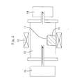
- FIG. 2 is a cross-sectional view illustrating a structure for an annealing furnace for use in the present invention.
- the furnace includes chamber 50, substrate holder 51, induction heating coil 52, gas supply system 53 and gas exhaust system 54.
- the chamber 50 may be made of quartz, while the holder 51 may be made of carbon, for example.
- the holder 51 is disposed inside the chamber 50 to place the SiC substrate 11 thereon.
- the coil 52 should heat the holder 51 and substrate 11 with radio frequency power.
- the pressure inside the chamber 50 is reduced to a vacuum under 10 -6 Pa.
- an annealing ambient gas is supplied from the gas supply system 53 into the chamber 50.
- the flow rate of the hydrogen gas is set to 2 l/min
- the pressure inside the chamber 50 during the annealing is fixed at the atmospheric pressure
- a power of 20 kW is applied to the coil 52 at a frequency of 20.0 kHz, thereby heating the SiC substrate 11 to 1600°C.
- the surface part of the SiC substrate 11 is etched away at a rate of 2 ⁇ m/hr within the hydrogen ambient.
- the concurrent anneal-etch process is performed for 30 minutes, thereby removing the upper doped layer 12b with the thickness of 1 ⁇ m.
- FIG. 1C is a cross-sectional view illustrating a structure of the SiC substrate 11 when the concurrent anneal-etch process is finished. As shown in FIG. 1C, the upper doped layer 12b has been etched away completely and the uppermost peak Prp7 is located almost at the surface of the SiC substrate 11.
- FIG. 3 is a graph illustrating the dopant concentration profile in the SiC substrate 11, which was subjected to the concurrent anneal-etch process of the first embodiment, as a result of secondary ion mass spectrometry (SIMS).
- the dopant (i.e., Al in the illustrated embodiment) concentration at the surface of the SiC substrate 11 is almost equal to the concentration at the uppermost peak Prp7 . That is to say, it can be seen that the dopant concentration at the surface was controlled to a desired value.
- the SiC substrate 11 is heated to and kept at an elevated temperature with hydrogen gas supplied into the chamber.
- the annealing process can be performed to repair the implant-induced damage while the surface part of the SiC substrate 11 is being etched away.
- no additional damage is done on the remaining part of the SiC substrate 11 and yet the surface part of the SiC substrate 11 (i.e., the upper doped layer 12b ), which has been damaged most seriously through the ion implantation, can be removed.
- the damage that is too serious to repair even through annealing is hardly left.
- the doped layer of this embodiment is used as an active region for any of various types of devices, then the number of crystal imperfections existing in the surface region of the device can be much smaller and the device can exhibit far better electrical characteristics.
- the method of this embodiment is very effective. This is because it is usually hard to form a locally doped layer in situ only in a specified region of an SiC layer that is being grown epitaxially.
- the method of this embodiment makes it possible to form a doped layer at any place we like by implanting dopant ions into some part of an SiC substrate. Accordingly, not only discrete devices but also a group of devices to be integrated together on a single SiC substrate can be fabricated by this method.
- the SiC substrate prepared by the method of this embodiment as shown in FIG. 1C has almost the same degree of surface planarity as an SiC substrate that has been annealed by a known method using Ar gas. That is to say, even though the SiC substrate shown in FIG. 1C has been subjected to the concurrent anneal-etch process, the surface planarity thereof has not been affected.
- the annealing and etching processes are supposed to be carried out in parallel.
- the present invention is not limited to this specific example, but should be construed to encompass an alternative embodiment in which the annealing process is performed first using Argon gas, for example, and then the etching process is carried out using hydrogen gas, for example. But it is nonetheless true that the present invention is applicable particularly effectively to the concurrent anneal-etch process, because the process efficiency and degree of damage repair improve significantly in that case.
- the present invention also realizes arbitrary control over the dopant concentration at the surface of the SiC substrate.
- part of the SiC substrate, which is located over the uppermost one of the several dopant concentration peaks formed by the multiple ion implantation processes, is supposed to be removed.
- the uppermost peak does not always have to be chosen. Rather, so long as the relationship between the ion implantation conditions and the dopant concentration profile formed in the substrate is known beforehand, the substrate may be etched away to any desired depth associated with any arbitrary dopant concentration peak.
- hydrogen gas is used as an exemplary etching gas for removing the surface part of the SiC substrate.
- the hydrogen gas is not the only one available according to the present invention.
- examples of other qualified gases include halogen gases like chlorine, fluorine and bromine gases and interhalogen gases such as ClF 3 gas. In any case, the effects of the foregoing embodiment are also attainable.
- the doped layer 12 formed in the upper part of the SiC substrate 11 in the foregoing embodiment may be replaced with an SiC single crystal layer that has been grown epitaxially on the SiC substrate 11 . That is to say, where an SiC substrate is used, part of the SiC substrate itself may be used as a semiconductor layer to which the present invention is applied. Or an SiC layer that has been grown epitaxially on the SiC substrate may be the semiconductor layer of the present invention. Generally speaking, though, a semiconductor layer grown epitaxially shows crystallinity superior to that of a semiconductor layer formed by a doping process. Thus, the semiconductor layer should preferably be grown epitaxially to obtain a device with a high breakdown voltage and good radio frequency characteristics.
- the annealing process is performed using the hydrogen gas as specified for the foregoing embodiment or using a mixture obtained by adding hydrogen or halogen gas to a rare gas of argon, for example, the intended damage repair and selective etching effects are also attainable.
- the concurrent anneal-etch process is carried out with the hydrogen gas supplied at a constant flow rate.
- the present invention is still effective even if the flow rate of the hydrogen gas is changed during the annealing process.
- a p-type doped layer is formed by implanting Al ions.
- ions of an n-type dopant such as nitrogen (N) or phosphorus (P) may be implanted into the SiC substrate instead.
- ions of another p-type dopant like boron (B), not aluminum (Al) may be implanted thereto. Even so, the same effects are attainable by performing the concurrent anneal-etch process of this embodiment.
- the ion implantation processes are performed seven times at mutually different accelerating voltages.
- the concurrent anneal-etch process of this embodiment is also effectively applicable to the dopant concentration control of, and the removal of seriously damaged part from, the substrate.
- a hexagonal 6H-SiC substrate is used as a substrate to be processed.
- any other hexagonal SiC substrate or a cubic 3C-SiC substrate may also be used.
- an Si 1-x-y Ge x C y or Si 1-y C y (where 0 ⁇ x ⁇ 1, 0.001 ⁇ y ⁇ 1) layer, formed on/in an Si substrate, is used as an active region, a dopant introduced into the Si 1-x-y Ge x C y or Si 1-y C y layer hardly diffuses even after the layer has been annealed.
- the method of this embodiment is also applicable to forming a device like this including a semiconductor layer that contains Si and C.
- the semiconductor layer containing Si and C may be either an integral part of the substrate or separately formed on a substrate of sapphire, quartz, etc.
- the surface part of the SiC substrate is removed by heating the substrate to an elevated temperature and supplying hydrogen gas thereto.
- the surface part of the SiC substrate is removable by any other technique.
- the surface part is also removable as intended if the substrate being heated is exposed to plasma, light, radicals or electrons. In these cases, the surface part is removed by utilizing a physical action. Even so, if the SiC substrate is heated to a certain high temperature, the surface part of the substrate is removable without doing so much damage on the substrate.
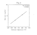
- FIG. 4 is a graph illustrating, based on the experimental data I collected, how the etch rate of the SiC substrate changes with the temperature of the substrate.
- the abscissa indicates the temperature (°C) of the SiC substrate, while the ordinate indicates the etch rate ( ⁇ m/hr).
- the flow rate of hydrogen gas is set to 3 l/min.
- the etch rate goes on increasing linearly. This is probably because the SiC etching reaction by hydrogen atoms or molecules is promoted by the temperature rise.
- the SiC substrate should preferably have a temperature between 500°C and 2300°C, both inclusive.
- the reason is as follows. On the one hand, if the substrate temperature is lower than 500°C, the hydrogen atoms cannot break the SiC bonds easily. On the other hand, if the substrate temperature exceeds 2300°C, then the SiC substrate itself might be decomposed unintentionally.
- the substrate temperature is preferably 1300°C or more. This is because I found that if the substrate temperature was less than 1300°C, the damage done on the SiC substrate could not be repaired sufficiently.
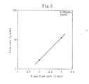
- FIG. 5 is a graph illustrating, based on the experimental data I collected, how the etch rate of the SiC substrate changes with the flow rate of the hydrogen gas.
- the abscissa indicates the flow rate (l/min) of the hydrogen gas, while the ordinate indicates the etch rate ( ⁇ m/hr).
- the temperature of the SiC substrate is fixed to at 1600 °C.
- the higher the flow rate of the hydrogen gas the higher the etch rate. This is probably because as the flow rate of the hydrogen gas rises, the hydrogen atoms or molecules, contributing to the etching reaction of the SiC substrate, increase their numbers, or density.
- the flow rate of hydrogen gas can be used as convenient parameters for controlling the etch rate of the SiC substrate.
- the hydrogen gas preferably has a flow rate between 0.001 l/min and 10 l/min, both inclusive. This is because if the flow rate of the hydrogen gas is less than 0.001 l/min, then the etch rate will be too low to remove the desired surface part of the SiC substrate. However, if the flow rate of hydrogen gas exceeds 10 l/min, then the etch rate will be too high to control the thickness of that part removed from the SiC substrate accurately.
- the etch rate is preferably 10 nm/min or more. Then, the surface part with the low dopant concentration can be accurately removed from the SiC substrate that has been subjected to the ion implantation processes at respective energies falling within a normal range of 1 keV to 10 MeV.
- This embodiment relates to a method for forming a Schottky diode by utilizing the concurrent anneal-etch technique of the first embodiment.
- FIGS. 6A through 6C are cross-sectional views illustrating respective process steps for forming a Schottky diode according to the second embodiment.
- an n + -type SiC substrate 21 prepared by heavily doping a 6H-SiC substrate with nitrogen, is placed in the reaction chamber of a CVD apparatus and subjected to a CVD process.
- the SiC substrate 21 has a (0001) off-axis plane as its principal surface.
- an undoped SiC layer is epitaxially grown to a thickness of about 5 ⁇ m on the n + -type SiC substrate 21.
- nitrogen (N) ions are implanted multiple times into the SiC layer by the method of the first embodiment, thereby forming an n-type doped layer 22 .
- the upper part of the doped layer 22 becomes an upper lightly doped layer 22b (with a thickness of about 1 ⁇ m), while the lower part thereof becomes an n-type lower doped layer 22a (with a thickness of about 4 ⁇ m) as in the structure shown in FIG. 1A .
- a peak of the concentration of N atoms introduced is located at the bottom of the epitaxial layer 22 (i.e., at the surface of the SiC substrate 21 ).
- the concentration of the n-type dopant (e.g., nitrogen) in the n + -type SiC substrate 21 is about 1 ⁇ 10 18 atoms ⁇ cm -3
- the average N concentration in the entire doped layer 22 is about 1 ⁇ 10 16 atoms ⁇ cm -3 .
- the SiC substrate 21 is placed in the chamber of an annealing furnace with a structure such as that shown in FIG. 2 . Then, the implant-induced damage done on the doped layer 22 is repaired and the upper part 22b of the doped layer 22 is etched away under the conditions specified for the first embodiment.
- the flow rate of hydrogen gas is set to 2 l/min, the pressure inside the chamber is fixed at the atmospheric pressure and the substrate is heated to and kept at 1600°C. This anneal-etch process is performed for about 30 minutes under these conditions, thereby removing the upper doped layer 22b almost completely.
- a nickel (Ni) film to be an electrode is deposited on the backside of the n + -type SiC substrate 21 using a vacuum evaporation apparatus. Then, the substrate is annealed at 1000°C for three minutes to form a backside electrode 23 that makes an ohmic contact with the SiC substrate 21 .
- a silicon dioxide film is deposited on the substrate and partially removed to form a girdling 24 .
- a surface electrode 25 of gold (Au) is formed thereon as a Schottky electrode to fill in the opening of the girdling 24 .
- the upper part 22b of the doped layer 22 is etched away.
- the process can be controlled in such a manner that the bottom of the surface electrode 25 is in contact with the part of the doped layer 22 with the highest dopant concentration as shown in FIG. 1A. That is to say, the dopant (N in this case) concentration at the surface of the lower doped layer 22a, which remains after the upper part 22b has been removed, can be controlled to a concentration required for making a Schottky contact.
- the upper part 22b which has been seriously damaged (or has a lot of defects) as a result of the ion implantation processes, is etched away.
- the region located right under the surface electrode 25 as a Schottky electrode has good enough crystallinity. Consequently, unlike a known Schottky diode on an SiC substrate, whose breakdown voltage decreases probably because a current flows due to the existence of defects under the surface electrode, the diode can maintain a high breakdown voltage and can exhibit excellent characteristics as a power diode.
- This embodiment relates to a method for forming a MISFET by utilizing the concurrent anneal-etch process of the first embodiment.
- FIGS. 7A through 7C are cross-sectional views illustrating respective process steps for forming a MISFET according to the third embodiment.
- an implant mask 32 of tungsten for example, is defined on an n-type SiC substrate 31 , which may be a 6H-SiC substrate with a (0001) off-axis plane as its principal surface.
- This mask covers part of the substrate 31 to be a channel region for a MISFET but does not cover other parts thereof to be source/drain regions.
- Al ions are implanted from over the mask 32 into the SiC substrate 31 a number of times as in the embodiment illustrated in FIGS. 1A through 1C, thereby forming a p-type source/drain doped layer 33.
- the upper part of the doped layer 33 becomes an upper lightly doped layer 33b (with a thickness of about 1 ⁇ m), while the lower part thereof becomes a p-type lower doped layer 33a (with a thickness of about 4 ⁇ m) as in the structure shown in FIG. 1A.
- the SiC substrate 31 is placed in the chamber of an annealing furnace with a structure such as that shown in FIG. 2 . Then, the implant-induced damage done on the source/drain doped layer 33 is repaired and the upper part 33b of the doped layer 33 is etched away under the conditions specified for the first embodiment.
- the flow rate of hydrogen gas is set to 2 l/min, the pressure inside the chamber is fixed at the atmospheric pressure and the substrate is heated to and kept at 1600°C.
- This anneal-etch process is performed for about 30 minutes under these conditions, thereby removing the upper doped layer 33b and another part of the SiC substrate 31 located between the right- and left-hand-side parts of the upper doped layer 33b .
- the lower doped layer 33a will be left as source/drain regions for a MISFET.
- a thermal oxide film 35 to be a gate insulating film is formed on the substrate, and then a gate electrode 34 is formed out of a nickel film so as to cover the channel region. Subsequently, parts of the thermal oxide film 35, now covering the source/drain regions, are removed. Instead, source/drain electrodes 36, making an ohmic contact with the lower doped layer 33a as source/drain regions, are formed out of a nickel film to fill in the openings. In this process step, the substrate is annealed at 1000°C for three minutes to make the ohmic contact.
- the lower doped layer 33a, or source/drain regions is not self-aligned with the gate electrode 34 .
- a gate electrode provided for a MISFET as a power electronic device normally has a gate length of 1 ⁇ m or more. Accordingly, even if the source/drain regions and gate electrode are misaligned with each other by about 0.15 ⁇ m due to the mask-to-mask placement error, the operation of the resultant MISFET is hardly affected.
- n-channel MISFET can be formed.
- At least those parts of the SiC substrate 31 in which the source/drain doped layer 33 is formed in the illustrated embodiment, may be included in an epitaxial layer on the SiC substrate.
- the inventive etching method is naturally applicable to forming a MESFET or a highvoltage device like an ACCUFET (accumulation mode FET) as can be easily understood from the description of the second and third embodiments.
- ACCUFET accumulation mode FET
Landscapes
- Electrodes Of Semiconductors (AREA)
- Drying Of Semiconductors (AREA)
- Insulated Gate Type Field-Effect Transistor (AREA)
Applications Claiming Priority (2)
| Application Number | Priority Date | Filing Date | Title |
|---|---|---|---|
| JP2000151243A JP2001332508A (ja) | 2000-05-23 | 2000-05-23 | 半導体素子の製造方法 |
| JP2000151243 | 2000-05-23 |
Publications (2)
| Publication Number | Publication Date |
|---|---|
| EP1160845A2 true EP1160845A2 (de) | 2001-12-05 |
| EP1160845A3 EP1160845A3 (de) | 2002-11-27 |
Family
ID=18656834
Family Applications (1)
| Application Number | Title | Priority Date | Filing Date |
|---|---|---|---|
| EP01112273A Ceased EP1160845A3 (de) | 2000-05-23 | 2001-05-18 | Verfahren zur Herstellung von einem Halbleiterbauelement aus Siliziumkarbid |
Country Status (3)
| Country | Link |
|---|---|
| US (1) | US20010046757A1 (de) |
| EP (1) | EP1160845A3 (de) |
| JP (1) | JP2001332508A (de) |
Cited By (2)
| Publication number | Priority date | Publication date | Assignee | Title |
|---|---|---|---|---|
| EP1641029A1 (de) * | 2004-09-27 | 2006-03-29 | STMicroelectronics S.r.l. | Verfahren zur Herstellung eines Schottky-Kontakts auf einem Halbleitersubstrat |
| EP3223302A4 (de) * | 2014-11-18 | 2018-07-25 | Toyo Tanso Co., Ltd. | Sic-substratbehandlungsverfahren |
Families Citing this family (18)
| Publication number | Priority date | Publication date | Assignee | Title |
|---|---|---|---|---|
| CA2474883A1 (en) * | 2002-02-08 | 2003-08-14 | Cree, Inc. | Methods of treating a silicon carbide substrate for improved epitaxial deposition |
| US7138291B2 (en) * | 2003-01-30 | 2006-11-21 | Cree, Inc. | Methods of treating a silicon carbide substrate for improved epitaxial deposition and resulting structures and devices |
| KR101008597B1 (ko) * | 2003-04-25 | 2011-01-17 | 스미토모덴키고교가부시키가이샤 | 반도체 장치의 제조 방법 |
| JP2006332180A (ja) * | 2005-05-24 | 2006-12-07 | Sumitomo Electric Ind Ltd | 炭化珪素半導体装置の製造方法 |
| JP2008153442A (ja) * | 2006-12-18 | 2008-07-03 | Renesas Technology Corp | 半導体装置の製造方法 |
| WO2009048997A1 (en) * | 2007-10-12 | 2009-04-16 | The Government Of The United States Of America, As Represented By The Secretary Of The Navy | Producing epitaxial layers with low basal plane dislocation concentrations |
| JP2010177465A (ja) * | 2009-01-29 | 2010-08-12 | Oki Semiconductor Co Ltd | 半導体装置、及びその製造方法 |
| JP2012004269A (ja) * | 2010-06-16 | 2012-01-05 | Sumitomo Electric Ind Ltd | 炭化珪素半導体装置の製造方法および炭化珪素半導体装置の製造装置 |
| CN103477439B (zh) | 2010-09-06 | 2014-12-10 | 松下电器产业株式会社 | 半导体装置及其制造方法 |
| JP5787655B2 (ja) * | 2010-11-26 | 2015-09-30 | 三菱電機株式会社 | 炭化珪素半導体装置およびその製造方法 |
| US9362370B2 (en) | 2012-10-30 | 2016-06-07 | Panasonic Intellectual Property Management Co., Ltd. | Silicon carbide semiconductor device having nitrogen-containing silicon alloy for ohmic contact to P-type impurity region |
| CN103033276B (zh) * | 2012-12-27 | 2014-07-02 | 长安大学 | 碳化硅温度传感器及其制造方法 |
| US9768259B2 (en) * | 2013-07-26 | 2017-09-19 | Cree, Inc. | Controlled ion implantation into silicon carbide using channeling and devices fabricated using controlled ion implantation into silicon carbide using channeling |
| WO2015064256A1 (ja) * | 2013-10-28 | 2015-05-07 | 富士電機株式会社 | 炭化シリコン半導体装置及びその製造方法 |
| JP6311384B2 (ja) | 2014-03-24 | 2018-04-18 | 三菱電機株式会社 | 炭化珪素半導体装置の製造方法 |
| DE112015006240T5 (de) * | 2015-07-30 | 2017-11-09 | Fuji Electric Co., Ltd. | HERSTELLUNGSVERFAHREN EINES SiC-SUBSTRATS |
| CN108292605B (zh) | 2016-06-24 | 2021-08-27 | 富士电机株式会社 | 半导体装置的制造方法和半导体装置 |
| IT202300010203A1 (it) * | 2023-05-19 | 2024-11-19 | Consiglio Nazionale Ricerche | Un transistor di potenza per un dispositivo a semiconduttore |
Family Cites Families (5)
| Publication number | Priority date | Publication date | Assignee | Title |
|---|---|---|---|---|
| US5087576A (en) * | 1987-10-26 | 1992-02-11 | North Carolina State University | Implantation and electrical activation of dopants into monocrystalline silicon carbide |
| WO1999017345A1 (de) * | 1997-09-30 | 1999-04-08 | Infineon Technologies Ag | Verfahren zum thermischen ausheilen von durch implantation dotierten siliziumcarbid-halbleitern |
| DE19808246B4 (de) * | 1998-02-27 | 2004-05-13 | Daimlerchrysler Ag | Verfahren zur Herstellung eines mikroelektronischen Halbleiterbauelements mittels Ionenimplatation |
| DE19808245C1 (de) * | 1998-02-27 | 1999-06-24 | Daimler Chrysler Ag | Verfahren zur Herstellung eines mikroelektronischen Halbleiterbauelements |
| JP3344562B2 (ja) * | 1998-07-21 | 2002-11-11 | 富士電機株式会社 | 炭化けい素半導体装置の製造方法 |
-
2000
- 2000-05-23 JP JP2000151243A patent/JP2001332508A/ja active Pending
-
2001
- 2001-05-18 US US09/861,065 patent/US20010046757A1/en not_active Abandoned
- 2001-05-18 EP EP01112273A patent/EP1160845A3/de not_active Ceased
Cited By (2)
| Publication number | Priority date | Publication date | Assignee | Title |
|---|---|---|---|---|
| EP1641029A1 (de) * | 2004-09-27 | 2006-03-29 | STMicroelectronics S.r.l. | Verfahren zur Herstellung eines Schottky-Kontakts auf einem Halbleitersubstrat |
| EP3223302A4 (de) * | 2014-11-18 | 2018-07-25 | Toyo Tanso Co., Ltd. | Sic-substratbehandlungsverfahren |
Also Published As
| Publication number | Publication date |
|---|---|
| JP2001332508A (ja) | 2001-11-30 |
| US20010046757A1 (en) | 2001-11-29 |
| EP1160845A3 (de) | 2002-11-27 |
Similar Documents
| Publication | Publication Date | Title |
|---|---|---|
| EP1160845A2 (de) | Verfahren zur Herstellung von einem Halbleiterbauelement aus Siliziumkarbid | |
| US5173761A (en) | Semiconducting polycrystalline diamond electronic devices employing an insulating diamond layer | |
| US6221700B1 (en) | Method of manufacturing silicon carbide semiconductor device with high activation rate of impurities | |
| US7718519B2 (en) | Method for manufacturing silicon carbide semiconductor element | |
| EP1032048B1 (de) | Herstellungsverfahren für Halbleiterbauelement mit isoliertem Gate | |
| US7982224B2 (en) | Semiconductor device with silicon carbide epitaxial layer including dopant profiles for reducing current overconcentration | |
| JP4418794B2 (ja) | 炭化珪素半導体素子の製造方法 | |
| JP5119806B2 (ja) | 炭化珪素半導体装置およびその製造方法 | |
| JP4581270B2 (ja) | SiC半導体のイオン注入層及びその製造方法 | |
| JP3184320B2 (ja) | ダイヤモンド電界効果トランジスタ | |
| JP4463448B2 (ja) | SiC基板及びSiC半導体素子の製造方法 | |
| US20100029053A1 (en) | Method of manufacturing semiconductor device | |
| EP2117036A1 (de) | Verfahren zur herstellung eines halbleiterbauelements und halbleiterbauelement | |
| JP2005303010A (ja) | 炭化珪素素子及びその製造方法 | |
| CA2636776A1 (en) | Method of manufacturing silicon carbide semiconductor device | |
| US8148717B2 (en) | Manufacturing method for semiconductor device and semiconductor device | |
| EP2015348B1 (de) | Herstellungsverfahren einer SiC-Halbleitervorrichtung | |
| JP2006066439A (ja) | 半導体装置およびその製造方法 | |
| JP2003234301A (ja) | 半導体基板、半導体素子及びその製造方法 | |
| JP4842527B2 (ja) | 半導体装置の製造方法 | |
| US20090159896A1 (en) | Silicon carbide mosfet devices and methods of making | |
| US7867882B2 (en) | Method of manufacturing silicon carbide semiconductor device | |
| JP3972450B2 (ja) | 炭化珪素半導体装置の製造方法 | |
| CN100593243C (zh) | Mosfet以及mosfet的制造方法 | |
| US20060197120A1 (en) | Gate electrode for semiconductor devices |
Legal Events
| Date | Code | Title | Description |
|---|---|---|---|
| PUAI | Public reference made under article 153(3) epc to a published international application that has entered the european phase |
Free format text: ORIGINAL CODE: 0009012 |
|
| AK | Designated contracting states |
Kind code of ref document: A2 Designated state(s): AT BE CH CY DE DK ES FI FR GB GR IE IT LI LU MC NL PT SE TR |
|
| AX | Request for extension of the european patent |
Free format text: AL;LT;LV;MK;RO;SI |
|
| 17P | Request for examination filed |
Effective date: 20020429 |
|
| PUAL | Search report despatched |
Free format text: ORIGINAL CODE: 0009013 |
|
| AK | Designated contracting states |
Kind code of ref document: A3 Designated state(s): AT BE CH CY DE DK ES FI FR GB GR IE IT LI LU MC NL PT SE TR |
|
| AX | Request for extension of the european patent |
Free format text: AL;LT;LV;MK;RO;SI |
|
| RIC1 | Information provided on ipc code assigned before grant |
Free format text: 7H 01L 21/265 A, 7H 01L 21/329 B, 7H 01L 21/336 B, 7H 01L 21/331 B |
|
| 17Q | First examination report despatched |
Effective date: 20030403 |
|
| AKX | Designation fees paid |
Designated state(s): CH DE DK ES FI FR GB GR IE IT LI LU MC NL PT SE TR |
|
| STAA | Information on the status of an ep patent application or granted ep patent |
Free format text: STATUS: THE APPLICATION HAS BEEN REFUSED |
|
| 18R | Application refused |
Effective date: 20051027 |