EP1162869A2 - Tuner, dessen "RF-Input"-Einschlussbeinchen sich nicht auf dem Rand befindet - Google Patents
Tuner, dessen "RF-Input"-Einschlussbeinchen sich nicht auf dem Rand befindet Download PDFInfo
- Publication number
- EP1162869A2 EP1162869A2 EP01401396A EP01401396A EP1162869A2 EP 1162869 A2 EP1162869 A2 EP 1162869A2 EP 01401396 A EP01401396 A EP 01401396A EP 01401396 A EP01401396 A EP 01401396A EP 1162869 A2 EP1162869 A2 EP 1162869A2
- Authority
- EP
- European Patent Office
- Prior art keywords
- printed circuit
- circuit board
- tuner
- signal
- shielding means
- Prior art date
- Legal status (The legal status is an assumption and is not a legal conclusion. Google has not performed a legal analysis and makes no representation as to the accuracy of the status listed.)
- Granted
Links
Images
Classifications
-
- H—ELECTRICITY
- H04—ELECTRIC COMMUNICATION TECHNIQUE
- H04N—PICTORIAL COMMUNICATION, e.g. TELEVISION
- H04N5/00—Details of television systems
- H04N5/44—Receiver circuitry for the reception of television signals according to analogue transmission standards
- H04N5/50—Tuning indicators; Automatic tuning control
-
- H—ELECTRICITY
- H05—ELECTRIC TECHNIQUES NOT OTHERWISE PROVIDED FOR
- H05K—PRINTED CIRCUITS; CASINGS OR CONSTRUCTIONAL DETAILS OF ELECTRIC APPARATUS; MANUFACTURE OF ASSEMBLAGES OF ELECTRICAL COMPONENTS
- H05K9/00—Screening of apparatus or components against electric or magnetic fields
- H05K9/0007—Casings
- H05K9/006—Casings specially adapted for signal processing applications, e.g. CATV, tuner, antennas amplifier
-
- H—ELECTRICITY
- H05—ELECTRIC TECHNIQUES NOT OTHERWISE PROVIDED FOR
- H05K—PRINTED CIRCUITS; CASINGS OR CONSTRUCTIONAL DETAILS OF ELECTRIC APPARATUS; MANUFACTURE OF ASSEMBLAGES OF ELECTRICAL COMPONENTS
- H05K1/00—Printed circuits
- H05K1/02—Details
- H05K1/14—Structural association of two or more printed circuits
- H05K1/141—One or more single auxiliary printed circuits mounted on a main printed circuit, e.g. modules, adapters
Definitions
- a tuner In a television tuner or other high-frequency receiving equipment, a tuner often includes a printed circuit board on which circuit components have been mounted and which is housed in a shielding case. It is common for low level RF signals, such as signals received from an antenna, CATV device or DSB device to be coupled to the receiver through a connector which permits the receiver to be easily connected or disconnected to/from this RF source. Such RF signals are then processed by a tuner section within the receiver.
- connection to the tuner it is desirable for the connection to the tuner to be direct and short to eliminate picking up extraneous signals and to prevent radiation of RF signals e.g., if the receiver is used on a cable system which has a large signal level. This would be the case if the RF signal input to the tuner had to be led in a long conductive path on the tuner printed circuit board to make contact at an edge connection of the board. Additionally, a long unshielded lead can cause an impedance mismatch at the termination points.
- a shielded modular tuner is horizontally mounted onto a chassis printed circuit board and is provided, through an aperture in the shield, with lead connections from the edge of the tuner printed circuit board to the chassis printed circuit board, for power supply, control signals, outputting a processed signal, etc.
- the RF signal is coupled to the tuner via a conductive pin extending from an RF signal conducting path on the chassis printed circuit board, passing through a second aperture in the shield, directly to the point on the tuner printed circuit board where the signal is to be inputted for tuner processing. In this way, the RF signal is injected directly into the tuner precisely where it is needed without being led along a longer path from the edge of the tuner printed circuit board, and without a shielded coaxial cable and accompanying connectors.
- tuner assemblies have a tuner printed circuit board(s) enclosed in shielding boxes which surround the tuner print circuit board(s) except for wiring terminals for interconnection of the tuner printed circuit board(s) to other circuitry, and is known in the prior art.
- the tuner printed circuit board(s) and components which are disposed upon the tuner printed circuit board(s) within the shielded volume are shielded from electromagnetic interference caused by extraneous signals or fields. This is particularly important for RF signals coming from an antenna or other such source because the signal level is very low and the signal has not been further amplified.
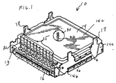
- a tuner 10 for a television set, VCR or other high-frequency equipment includes a tuner printed circuit board 12 on which circuit components (not shown) are mounted and with the circuit board 12 being mounted within a shielding case 14 having electrically conductive frame 14a, electrically conductive top cover 14b and electrically conductive bottom cover 14c assembled together by electrically conductive spring fingers 16 or the like.
- Tabs 18 are provided to mount tuner 10 to a chassis printed circuit board 20 and can be used to electrically ground shielding case 14 by soldering, twisting, or the like.
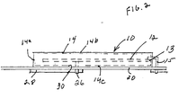
- Electrically conductive pins/leads 22 are provided coming from an edge of printed circuit board 12 for connection to respective electrically conductive paths 24 on chassis printed circuit board 20.
- an electrically conductive pin/lead 26 is connected at the tuner circuit input and extends away from the board 12, through aperture 30 in bottom plate 14c, and is connected to an RF signal carrying electrical conductor 28 disposed on chassis printed circuit board 20.
- the shielding effect of the body of shield 14 acts to shield electrical conductor 28 by its proximate presence. Still further, shielding can be provided to electrical conductor 28 by the close proximity of grounded printed circuit conductors (not shown) similar to practices used on tuner printed circuit boards.
- the RF signal is coupled to electrical conductor 28 by means of a coupling connector coupling the RF signal to the apparatus, through isolation barrier circuitry (not shown), if appropriate.
- the RF signal input is provided to the tuner in a short and direct path, without the cost of a coaxial cable and associated connector carrying the RF signal from the device RF signal input connector for the apparatus.
- circuit boards 12, 20 are planar and rigid, it is within the contemplation of the present invention that either or both circuit boards 12, 20 may not be rigid.
Landscapes
- Engineering & Computer Science (AREA)
- Signal Processing (AREA)
- Microelectronics & Electronic Packaging (AREA)
- Multimedia (AREA)
- Shielding Devices Or Components To Electric Or Magnetic Fields (AREA)
- Structure Of Receivers (AREA)
- Details Of Connecting Devices For Male And Female Coupling (AREA)
- Structures For Mounting Electric Components On Printed Circuit Boards (AREA)
- Combinations Of Printed Boards (AREA)
- Input Circuits Of Receivers And Coupling Of Receivers And Audio Equipment (AREA)
- Channel Selection Circuits, Automatic Tuning Circuits (AREA)
- Superheterodyne Receivers (AREA)
- Circuits Of Receivers In General (AREA)
Applications Claiming Priority (2)
| Application Number | Priority Date | Filing Date | Title |
|---|---|---|---|
| US09/590,910 US6404309B1 (en) | 2000-06-09 | 2000-06-09 | Tuner with non-edge RF input pin/lead |
| US590910 | 2000-06-09 |
Publications (4)
| Publication Number | Publication Date |
|---|---|
| EP1162869A2 true EP1162869A2 (de) | 2001-12-12 |
| EP1162869A3 EP1162869A3 (de) | 2008-04-02 |
| EP1162869B1 EP1162869B1 (de) | 2009-10-21 |
| EP1162869B8 EP1162869B8 (de) | 2010-03-10 |
Family
ID=24364233
Family Applications (1)
| Application Number | Title | Priority Date | Filing Date |
|---|---|---|---|
| EP01401396A Expired - Lifetime EP1162869B8 (de) | 2000-06-09 | 2001-05-29 | Tuner, dessen "RF-Input"-Einschlussbeinchen sich nicht auf dem Rand befindet |
Country Status (8)
| Country | Link |
|---|---|
| US (1) | US6404309B1 (de) |
| EP (1) | EP1162869B8 (de) |
| JP (1) | JP4582961B2 (de) |
| KR (1) | KR100824822B1 (de) |
| CN (1) | CN1225157C (de) |
| AT (1) | ATE446668T1 (de) |
| DE (1) | DE60140233D1 (de) |
| MX (1) | MXPA01005823A (de) |
Families Citing this family (13)
| Publication number | Priority date | Publication date | Assignee | Title |
|---|---|---|---|---|
| KR100395562B1 (ko) * | 2001-10-10 | 2003-08-21 | 삼성전자주식회사 | 방송신호 수신장치용 모듈레이터/아이에프회로 일체형튜너블록 |
| JP4703104B2 (ja) * | 2003-06-06 | 2011-06-15 | 株式会社東芝 | 通信端末装置 |
| JP4381038B2 (ja) * | 2003-06-06 | 2009-12-09 | 株式会社東芝 | 送受信装置およびケーブルモデムモジュール装置 |
| JP4621466B2 (ja) * | 2004-09-30 | 2011-01-26 | 株式会社東芝 | チューナ装置 |
| JP4725737B2 (ja) * | 2006-09-20 | 2011-07-13 | ミツミ電機株式会社 | チューナ装置 |
| KR101349274B1 (ko) * | 2007-07-05 | 2014-01-10 | 엘지이노텍 주식회사 | 튜너 |
| JP4938073B2 (ja) * | 2009-11-10 | 2012-05-23 | シャープ株式会社 | 放送受信装置 |
| JP2011139321A (ja) * | 2009-12-28 | 2011-07-14 | Sony Corp | チューナモジュールおよび受信装置 |
| KR101124021B1 (ko) | 2010-06-25 | 2012-03-23 | 삼성전기주식회사 | 몰드핀 결합 어셈블리 및 이를 포함하는 튜너 |
| JP2012059605A (ja) * | 2010-09-10 | 2012-03-22 | Alps Electric Co Ltd | 高周波モジュール |
| KR20130035675A (ko) * | 2011-09-30 | 2013-04-09 | 삼성전기주식회사 | 튜너 모듈 |
| US8747121B1 (en) | 2013-01-24 | 2014-06-10 | Cresta Technology Corporation | Television tuner module having a shielded housing mounted on an outer circuit board and having an inner circuit board with a tuner chip |
| KR101762627B1 (ko) | 2015-11-17 | 2017-08-14 | 하나 마이크론(주) | 반도체 패키지 및 그 제조 방법 |
Family Cites Families (12)
| Publication number | Priority date | Publication date | Assignee | Title |
|---|---|---|---|---|
| JPS59177243U (ja) * | 1983-05-12 | 1984-11-27 | 日本電気ホームエレクトロニクス株式会社 | 電子機器 |
| DE8319031U1 (de) * | 1983-07-01 | 1983-09-29 | Deutsche Thomson-Brandt Gmbh, 7730 Villingen-Schwenningen | Hf-baugruppen integriert in ein einplatinenchassis eines fernsehgeraetes |
| JPH0411349Y2 (de) * | 1985-12-03 | 1992-03-19 | ||
| JPS6358462U (de) * | 1986-10-02 | 1988-04-19 | ||
| JPH0279498A (ja) * | 1988-09-14 | 1990-03-20 | Toshiba Corp | チューナ構造 |
| JPH0380593A (ja) * | 1989-08-23 | 1991-04-05 | Aisin Seiki Co Ltd | 混成集積回路のハイブリット接合方法 |
| JP3093352B2 (ja) * | 1991-09-05 | 2000-10-03 | 名古屋電機工業株式会社 | 移動物体検知装置 |
| JPH05343141A (ja) * | 1992-06-10 | 1993-12-24 | Matsushita Electric Ind Co Ltd | プリント基板接続装置 |
| JP3279030B2 (ja) * | 1993-12-27 | 2002-04-30 | ソニー株式会社 | 遮蔽部材及び遮蔽部材の製造方法 |
| TW443717U (en) * | 1996-06-28 | 2001-06-23 | Sharp Kk | Tuner structure and cable modem tuner using the same |
| JP3208076B2 (ja) * | 1996-12-02 | 2001-09-10 | アルプス電気株式会社 | シールドケース |
| DE19809312A1 (de) * | 1998-03-05 | 1999-09-23 | Grundig Ag | Hochfrequenzdichtes Gehäuse |
-
2000
- 2000-06-09 US US09/590,910 patent/US6404309B1/en not_active Expired - Lifetime
-
2001
- 2001-05-29 EP EP01401396A patent/EP1162869B8/de not_active Expired - Lifetime
- 2001-05-29 DE DE60140233T patent/DE60140233D1/de not_active Expired - Lifetime
- 2001-05-29 AT AT01401396T patent/ATE446668T1/de not_active IP Right Cessation
- 2001-06-07 JP JP2001172603A patent/JP4582961B2/ja not_active Expired - Fee Related
- 2001-06-07 KR KR1020010031666A patent/KR100824822B1/ko not_active Expired - Fee Related
- 2001-06-08 MX MXPA01005823A patent/MXPA01005823A/es active IP Right Grant
- 2001-06-08 CN CNB01121466XA patent/CN1225157C/zh not_active Expired - Fee Related
Also Published As
| Publication number | Publication date |
|---|---|
| JP2002057589A (ja) | 2002-02-22 |
| KR20010111017A (ko) | 2001-12-15 |
| KR100824822B1 (ko) | 2008-04-23 |
| DE60140233D1 (de) | 2009-12-03 |
| EP1162869A3 (de) | 2008-04-02 |
| MXPA01005823A (es) | 2004-11-10 |
| CN1335746A (zh) | 2002-02-13 |
| EP1162869B8 (de) | 2010-03-10 |
| ATE446668T1 (de) | 2009-11-15 |
| US6404309B1 (en) | 2002-06-11 |
| CN1225157C (zh) | 2005-10-26 |
| EP1162869B1 (de) | 2009-10-21 |
| JP4582961B2 (ja) | 2010-11-17 |
Similar Documents
| Publication | Publication Date | Title |
|---|---|---|
| US5120258A (en) | Low inductance shielded cable to printed circuit board connection apparatus | |
| US5241135A (en) | Connector grounding terminal | |
| US6404309B1 (en) | Tuner with non-edge RF input pin/lead | |
| US6113422A (en) | Connector with circuit devices and indicators | |
| US4970625A (en) | Integrated module handle and chassis bulkhead for reducing electromagnetic interference emissions from circuit modules | |
| US20060134946A1 (en) | Electrical connector with horizontal ground plane | |
| US5388030A (en) | Metal module housing having a plurality of lugs formed therein for supporting and grounding a printed circuit board | |
| US20200395717A1 (en) | Compact Coaxial Cable Connector For Transmitting Super High Frequency Signals | |
| US7540780B2 (en) | Microphone connector | |
| KR20200143204A (ko) | 초고주파 신호 전송용 소형 커넥터 | |
| US20140268598A1 (en) | Electronic Device Having Connector With Integrated Shielding | |
| US7701309B2 (en) | Power inserter module | |
| US10396505B2 (en) | Filter connector | |
| CN112086785B (zh) | 用于传输超高频信号的紧凑型连接器 | |
| JP2003508936A (ja) | Emi抑制配線プレートを備えた電気部品の組立体及びその製造方法並びにemi抑制配線プレート | |
| EP1384320B1 (de) | Verfahren und gerät zur verringerung von elektromagnetischer strahlung | |
| US9356397B2 (en) | Connector and electronic system using the same | |
| US4999542A (en) | Data processing display terminal | |
| JP6901537B2 (ja) | 同軸コネクタ装置 | |
| JPH07302989A (ja) | 電子・通信装置 | |
| JPH021905Y2 (de) | ||
| JPH05251583A (ja) | 高周波プリント板回路 | |
| TH2001001369A (th) | ตัวต่อเกราะชนิดติดตั้งบนแผง | |
| JP2002198109A (ja) | 電気通信モジュール | |
| JPH08222325A (ja) | プリント配線板へのフラット同軸ケーブルの接続法 |
Legal Events
| Date | Code | Title | Description |
|---|---|---|---|
| PUAI | Public reference made under article 153(3) epc to a published international application that has entered the european phase |
Free format text: ORIGINAL CODE: 0009012 |
|
| AK | Designated contracting states |
Kind code of ref document: A2 Designated state(s): AT BE CH CY DE DK ES FI FR GB GR IE IT LI LU MC NL PT SE TR |
|
| AX | Request for extension of the european patent |
Free format text: AL;LT;LV;MK;RO;SI |
|
| RAP1 | Party data changed (applicant data changed or rights of an application transferred) |
Owner name: THOMSON LICENSING |
|
| PUAL | Search report despatched |
Free format text: ORIGINAL CODE: 0009013 |
|
| AK | Designated contracting states |
Kind code of ref document: A3 Designated state(s): AT BE CH CY DE DK ES FI FR GB GR IE IT LI LU MC NL PT SE TR |
|
| AX | Request for extension of the european patent |
Extension state: AL LT LV MK RO SI |
|
| 17P | Request for examination filed |
Effective date: 20080930 |
|
| AKX | Designation fees paid |
Designated state(s): AT BE CH CY DE DK ES FI FR GB GR IE IT LI LU MC NL PT SE TR |
|
| GRAP | Despatch of communication of intention to grant a patent |
Free format text: ORIGINAL CODE: EPIDOSNIGR1 |
|
| GRAS | Grant fee paid |
Free format text: ORIGINAL CODE: EPIDOSNIGR3 |
|
| GRAA | (expected) grant |
Free format text: ORIGINAL CODE: 0009210 |
|
| AK | Designated contracting states |
Kind code of ref document: B1 Designated state(s): AT BE CH CY DE DK ES FI FR GB GR IE IT LI LU MC NL PT SE TR |
|
| REG | Reference to a national code |
Ref country code: GB Ref legal event code: FG4D |
|
| REG | Reference to a national code |
Ref country code: CH Ref legal event code: EP |
|
| REG | Reference to a national code |
Ref country code: IE Ref legal event code: FG4D |
|
| REF | Corresponds to: |
Ref document number: 60140233 Country of ref document: DE Date of ref document: 20091203 Kind code of ref document: P |
|
| REG | Reference to a national code |
Ref country code: GB Ref legal event code: 746 Effective date: 20091201 |
|
| RAP2 | Party data changed (patent owner data changed or rights of a patent transferred) |
Owner name: THOMSON LICENSING |
|
| NLV1 | Nl: lapsed or annulled due to failure to fulfill the requirements of art. 29p and 29m of the patents act | ||
| PG25 | Lapsed in a contracting state [announced via postgrant information from national office to epo] |
Ref country code: ES Free format text: LAPSE BECAUSE OF FAILURE TO SUBMIT A TRANSLATION OF THE DESCRIPTION OR TO PAY THE FEE WITHIN THE PRESCRIBED TIME-LIMIT Effective date: 20100201 Ref country code: FI Free format text: LAPSE BECAUSE OF FAILURE TO SUBMIT A TRANSLATION OF THE DESCRIPTION OR TO PAY THE FEE WITHIN THE PRESCRIBED TIME-LIMIT Effective date: 20091021 Ref country code: PT Free format text: LAPSE BECAUSE OF FAILURE TO SUBMIT A TRANSLATION OF THE DESCRIPTION OR TO PAY THE FEE WITHIN THE PRESCRIBED TIME-LIMIT Effective date: 20100222 Ref country code: SE Free format text: LAPSE BECAUSE OF FAILURE TO SUBMIT A TRANSLATION OF THE DESCRIPTION OR TO PAY THE FEE WITHIN THE PRESCRIBED TIME-LIMIT Effective date: 20091021 |
|
| PG25 | Lapsed in a contracting state [announced via postgrant information from national office to epo] |
Ref country code: BE Free format text: LAPSE BECAUSE OF FAILURE TO SUBMIT A TRANSLATION OF THE DESCRIPTION OR TO PAY THE FEE WITHIN THE PRESCRIBED TIME-LIMIT Effective date: 20091021 Ref country code: AT Free format text: LAPSE BECAUSE OF FAILURE TO SUBMIT A TRANSLATION OF THE DESCRIPTION OR TO PAY THE FEE WITHIN THE PRESCRIBED TIME-LIMIT Effective date: 20091021 |
|
| PG25 | Lapsed in a contracting state [announced via postgrant information from national office to epo] |
Ref country code: DK Free format text: LAPSE BECAUSE OF FAILURE TO SUBMIT A TRANSLATION OF THE DESCRIPTION OR TO PAY THE FEE WITHIN THE PRESCRIBED TIME-LIMIT Effective date: 20091021 |
|
| PLBE | No opposition filed within time limit |
Free format text: ORIGINAL CODE: 0009261 |
|
| STAA | Information on the status of an ep patent application or granted ep patent |
Free format text: STATUS: NO OPPOSITION FILED WITHIN TIME LIMIT |
|
| 26N | No opposition filed |
Effective date: 20100722 |
|
| PG25 | Lapsed in a contracting state [announced via postgrant information from national office to epo] |
Ref country code: GR Free format text: LAPSE BECAUSE OF FAILURE TO SUBMIT A TRANSLATION OF THE DESCRIPTION OR TO PAY THE FEE WITHIN THE PRESCRIBED TIME-LIMIT Effective date: 20100122 |
|
| PG25 | Lapsed in a contracting state [announced via postgrant information from national office to epo] |
Ref country code: MC Free format text: LAPSE BECAUSE OF NON-PAYMENT OF DUE FEES Effective date: 20100531 |
|
| REG | Reference to a national code |
Ref country code: CH Ref legal event code: PL |
|
| PG25 | Lapsed in a contracting state [announced via postgrant information from national office to epo] |
Ref country code: LI Free format text: LAPSE BECAUSE OF NON-PAYMENT OF DUE FEES Effective date: 20100531 Ref country code: CH Free format text: LAPSE BECAUSE OF NON-PAYMENT OF DUE FEES Effective date: 20100531 |
|
| PG25 | Lapsed in a contracting state [announced via postgrant information from national office to epo] |
Ref country code: IE Free format text: LAPSE BECAUSE OF NON-PAYMENT OF DUE FEES Effective date: 20100529 |
|
| PG25 | Lapsed in a contracting state [announced via postgrant information from national office to epo] |
Ref country code: CY Free format text: LAPSE BECAUSE OF FAILURE TO SUBMIT A TRANSLATION OF THE DESCRIPTION OR TO PAY THE FEE WITHIN THE PRESCRIBED TIME-LIMIT Effective date: 20091021 |
|
| PG25 | Lapsed in a contracting state [announced via postgrant information from national office to epo] |
Ref country code: NL Free format text: LAPSE BECAUSE OF FAILURE TO SUBMIT A TRANSLATION OF THE DESCRIPTION OR TO PAY THE FEE WITHIN THE PRESCRIBED TIME-LIMIT Effective date: 20091021 Ref country code: LU Free format text: LAPSE BECAUSE OF NON-PAYMENT OF DUE FEES Effective date: 20100529 |
|
| PG25 | Lapsed in a contracting state [announced via postgrant information from national office to epo] |
Ref country code: TR Free format text: LAPSE BECAUSE OF FAILURE TO SUBMIT A TRANSLATION OF THE DESCRIPTION OR TO PAY THE FEE WITHIN THE PRESCRIBED TIME-LIMIT Effective date: 20091021 |
|
| REG | Reference to a national code |
Ref country code: FR Ref legal event code: PLFP Year of fee payment: 16 |
|
| REG | Reference to a national code |
Ref country code: FR Ref legal event code: PLFP Year of fee payment: 17 |
|
| REG | Reference to a national code |
Ref country code: DE Ref legal event code: R082 Ref document number: 60140233 Country of ref document: DE Representative=s name: DEHNS, DE Ref country code: DE Ref legal event code: R082 Ref document number: 60140233 Country of ref document: DE Representative=s name: HOFSTETTER, SCHURACK & PARTNER PATENT- UND REC, DE |
|
| REG | Reference to a national code |
Ref country code: FR Ref legal event code: PLFP Year of fee payment: 18 |
|
| REG | Reference to a national code |
Ref country code: FR Ref legal event code: TP Owner name: THOMSON LICENSING DTV, FR Effective date: 20180830 |
|
| REG | Reference to a national code |
Ref country code: GB Ref legal event code: 732E Free format text: REGISTERED BETWEEN 20180927 AND 20181005 |
|
| REG | Reference to a national code |
Ref country code: DE Ref legal event code: R082 Ref document number: 60140233 Country of ref document: DE Representative=s name: DEHNS, DE Ref country code: DE Ref legal event code: R081 Ref document number: 60140233 Country of ref document: DE Owner name: INTERDIGITAL MADISON PATENT HOLDINGS, FR Free format text: FORMER OWNER: THOMSON LICENSING, BOULOGNE-BILLANCOURT, FR |
|
| PGFP | Annual fee paid to national office [announced via postgrant information from national office to epo] |
Ref country code: DE Payment date: 20190418 Year of fee payment: 19 Ref country code: IT Payment date: 20190418 Year of fee payment: 19 |
|
| PGFP | Annual fee paid to national office [announced via postgrant information from national office to epo] |
Ref country code: FR Payment date: 20190419 Year of fee payment: 19 |
|
| PGFP | Annual fee paid to national office [announced via postgrant information from national office to epo] |
Ref country code: GB Payment date: 20190423 Year of fee payment: 19 |
|
| REG | Reference to a national code |
Ref country code: DE Ref legal event code: R119 Ref document number: 60140233 Country of ref document: DE |
|
| GBPC | Gb: european patent ceased through non-payment of renewal fee |
Effective date: 20200529 |
|
| PG25 | Lapsed in a contracting state [announced via postgrant information from national office to epo] |
Ref country code: GB Free format text: LAPSE BECAUSE OF NON-PAYMENT OF DUE FEES Effective date: 20200529 Ref country code: FR Free format text: LAPSE BECAUSE OF NON-PAYMENT OF DUE FEES Effective date: 20200531 |
|
| PG25 | Lapsed in a contracting state [announced via postgrant information from national office to epo] |
Ref country code: DE Free format text: LAPSE BECAUSE OF NON-PAYMENT OF DUE FEES Effective date: 20201201 |
|
| PG25 | Lapsed in a contracting state [announced via postgrant information from national office to epo] |
Ref country code: IT Free format text: LAPSE BECAUSE OF NON-PAYMENT OF DUE FEES Effective date: 20200529 |