EP1163632B1 - Transducteur a ondes acoustiques de surface et systeme d'identification equipe de ce dernier - Google Patents
Transducteur a ondes acoustiques de surface et systeme d'identification equipe de ce dernier Download PDFInfo
- Publication number
- EP1163632B1 EP1163632B1 EP99915736A EP99915736A EP1163632B1 EP 1163632 B1 EP1163632 B1 EP 1163632B1 EP 99915736 A EP99915736 A EP 99915736A EP 99915736 A EP99915736 A EP 99915736A EP 1163632 B1 EP1163632 B1 EP 1163632B1
- Authority
- EP
- European Patent Office
- Prior art keywords
- dispersive
- signal
- acoustic wave
- transducers
- surface acoustic
- Prior art date
- Legal status (The legal status is an assumption and is not a legal conclusion. Google has not performed a legal analysis and makes no representation as to the accuracy of the status listed.)
- Expired - Lifetime
Links
Images


Classifications
-
- H—ELECTRICITY
- H04—ELECTRIC COMMUNICATION TECHNIQUE
- H04B—TRANSMISSION
- H04B5/00—Near-field transmission systems, e.g. inductive or capacitive transmission systems
- H04B5/70—Near-field transmission systems, e.g. inductive or capacitive transmission systems specially adapted for specific purposes
- H04B5/77—Near-field transmission systems, e.g. inductive or capacitive transmission systems specially adapted for specific purposes for interrogation
-
- H—ELECTRICITY
- H03—ELECTRONIC CIRCUITRY
- H03H—IMPEDANCE NETWORKS, e.g. RESONANT CIRCUITS; RESONATORS
- H03H9/00—Networks comprising electromechanical or electro-acoustic elements; Electromechanical resonators
- H03H9/46—Filters
- H03H9/64—Filters using surface acoustic waves
- H03H9/6406—Filters characterised by a particular frequency characteristic
-
- G—PHYSICS
- G06—COMPUTING OR CALCULATING; COUNTING
- G06K—GRAPHICAL DATA READING; PRESENTATION OF DATA; RECORD CARRIERS; HANDLING RECORD CARRIERS
- G06K19/00—Record carriers for use with machines and with at least a part designed to carry digital markings
- G06K19/06—Record carriers for use with machines and with at least a part designed to carry digital markings characterised by the kind of the digital marking, e.g. shape, nature, code
- G06K19/067—Record carriers with conductive marks, printed circuits or semiconductor circuit elements, e.g. credit or identity cards also with resonating or responding marks without active components
- G06K19/0672—Record carriers with conductive marks, printed circuits or semiconductor circuit elements, e.g. credit or identity cards also with resonating or responding marks without active components with resonating marks
- G06K19/0675—Record carriers with conductive marks, printed circuits or semiconductor circuit elements, e.g. credit or identity cards also with resonating or responding marks without active components with resonating marks the resonating marks being of the surface acoustic wave [SAW] kind
-
- H—ELECTRICITY
- H03—ELECTRONIC CIRCUITRY
- H03H—IMPEDANCE NETWORKS, e.g. RESONANT CIRCUITS; RESONATORS
- H03H9/00—Networks comprising electromechanical or electro-acoustic elements; Electromechanical resonators
- H03H9/02—Details
- H03H9/125—Driving means, e.g. electrodes, coils
- H03H9/145—Driving means, e.g. electrodes, coils for networks using surface acoustic waves
- H03H9/14544—Transducers of particular shape or position
- H03H9/14555—Chirped transducers
-
- H—ELECTRICITY
- H03—ELECTRONIC CIRCUITRY
- H03H—IMPEDANCE NETWORKS, e.g. RESONANT CIRCUITS; RESONATORS
- H03H9/00—Networks comprising electromechanical or electro-acoustic elements; Electromechanical resonators
- H03H9/30—Time-delay networks
- H03H9/42—Time-delay networks using surface acoustic waves
- H03H9/44—Frequency dependent delay lines, e.g. dispersive delay lines
-
- H—ELECTRICITY
- H03—ELECTRONIC CIRCUITRY
- H03H—IMPEDANCE NETWORKS, e.g. RESONANT CIRCUITS; RESONATORS
- H03H9/00—Networks comprising electromechanical or electro-acoustic elements; Electromechanical resonators
- H03H9/46—Filters
- H03H9/64—Filters using surface acoustic waves
- H03H9/6406—Filters characterised by a particular frequency characteristic
- H03H9/6416—SAW matched filters, e.g. surface acoustic wave compressors, chirped or coded surface acoustic wave filters
- H03H9/642—SAW transducers details for remote interrogation systems, e.g. surface acoustic wave transducers details for ID-tags
-
- H—ELECTRICITY
- H04—ELECTRIC COMMUNICATION TECHNIQUE
- H04B—TRANSMISSION
- H04B5/00—Near-field transmission systems, e.g. inductive or capacitive transmission systems
- H04B5/70—Near-field transmission systems, e.g. inductive or capacitive transmission systems specially adapted for specific purposes
- H04B5/73—Near-field transmission systems, e.g. inductive or capacitive transmission systems specially adapted for specific purposes for taking measurements, e.g. using sensing coils
-
- H—ELECTRICITY
- H04—ELECTRIC COMMUNICATION TECHNIQUE
- H04R—LOUDSPEAKERS, MICROPHONES, GRAMOPHONE PICK-UPS OR LIKE ACOUSTIC ELECTROMECHANICAL TRANSDUCERS; ELECTRIC HEARING AIDS; PUBLIC ADDRESS SYSTEMS
- H04R23/00—Transducers other than those covered by groups H04R9/00 - H04R21/00
Definitions
- the invention relates to a surface wave transducer device - also TAGs called - as well as identification systems in which this is used.
- Document US-A-5 469 170 shows a surface wave transducer device from a dispersive transmission device and a variety of non-dispersive transducers consists. An identification code is given by the distance the active transducers are fixed to each other.
- DE 42 17 049 discloses a passive surface sensor that can be queried wirelessly.
- energy is transmitted to the sensor via radio via a query device, the query being carried out by means of chirped transmission signals.
- the sensor points Converters and reflectors.
- the reflectors reflect the chirp signal in time staggered sequence, so that the sensor a staggered chirp signal to the Returns the interrogator.
- the surface wave sensor described above hereinafter also referred to as SAW (surface acoustic wave) or OFW (acoustic surface wave) sensor ) has a very high insertion loss due to the reflection principle on, for example, in the order of 50 dB.
- the signal would have to be so powerful be that it violates the usual requirements of the regulatory authorities, which limit the signal shapes and power spectrum of transmitters to a certain level, so that it does not lead to undesirable disturbances, such as, for example are also known from radar technology, but there because of important monitoring functions (Flight surveillance) in a certain frequency range become.
- a surface converter device is used proposed the features of claim 1. Advantageous further developments are described in the subclaims.
- the invention is based on the idea of a surface wave converter device a combination arrangement of a dispersive transducer device with to provide a non-dispersive converter device.
- a dispersive converter device is able to convert a surface wave pulse signal from a chirp signal to generate, which consists of the non-dispersive transducer device n transducers, received by and into a code pulse signal sequence that the surface wave transducer device identified, implemented.
- the pulse signal sequence is then emitted by the surface wave converter device via an antenna and can be accessed by an interrogation unit within an identification system received and evaluated with regard to the identification mark.
- An SAW converter device is characterized by considerable longer than previously known query distances, has a very large Bit capacity and is very easy to program.
- the large query distance and the correspondingly low insertion loss is due to the fact that the SAW converter device according to the invention when receiving a signal from a Interrogator once the interrogation signal in the dispersive SAW converter device converted into a time-compressed surface wave signal which is received by the non-dispersive transducer device.
- the non-dispersive transducer device also receives the interrogation signal and generates it corresponding SAW signals which are received by the dispersive converter become. After reception, it converts the surface waves into corresponding ones electromagnetic signals around. Due to the identical terms of the Signals from the dispersive converter device to the non-dispersive converter device and vice versa, two identical signals overlap on the output side, so that the code signal to be transmitted by the TAG has a larger signal power features.
- the TAG's response signal to an interrogation signal accordingly exists of two components, since both components are at the same time from the TAG are sent and both signal components over the identical signal form have, the TAG according to the invention has a higher power efficiency and the TAG transmission signal is considerably more powerful than the TAG signal at comparable SAW arrangements, the performance always being comparable Interrogator interrogation signals.
- the surface wave transducer device according to the invention advantageously has no reflectors, so that the insertion loss is considerably lower than with reflector arrangements.
- the insertion loss for known SAW TAGs is with reflector arrangement about 50 dB.
- As an interrogation signal it is expedient uses a chirp signal which is based on the inventive SAW-TAG is converted into a time-compressed pulse signal.
- the TAG response signal consists of time-compressed, time-shifted in a chirp interrogation signal Pulse signals, the modulation of the response signals from the programming the n-converter depends on the nondispersive converter arrangement. is for example a single converter of the n converters is not connected to the common bus lines connected, there is also no response signal from this converter. Such an answer can be understood as a logical "zero".
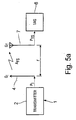
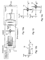
- TAG 1 shows a block unit diagram of an interrogator 1 consisting of a transmitter unit 2 and a receiver unit 3.
- the transmitter unit 2 is an antenna 4 and an antenna 5 is assigned to the receiving unit 3.
- the diagram shows an identification unit 6 (TAG) (TAG), also "passive TAG ".
- TAG 6 has a receiving antenna 7 and a transmitting antenna 8.
- the antennas 4 and 5 of the interrogation unit 1 as well as the antennas 7 and 8 can be made in one piece, i.e. the transmit and receive antennas are in each a single antenna unit.
- the interrogation unit 1 generates a signal in the transmission unit 2 and sends it via the antenna 4.
- the signal emitted by the antenna 4 is by means of the TAG antenna 7 received and the TAG transmits in response to the received signal a TAG own (identification) signal, which in turn is from the Receiving unit 3 of the interrogation unit 1 is received. So that such question-answer communication take place between the interrogation unit 1 and the TAG 6 maximum distance is possible with limited transmission power. Will this If the distance is exceeded, there is interference in the question-answer communication between the interrogator and the TAG.
- 2b shows the signal-to-noise ratio of the receiver of the interrogation unit a passive TAG.
- the invention TAG identification system for example, has a ⁇ of 100 W / W.
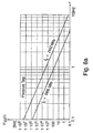
- FIG. 5 in turn shows part of FIG. 1 (FIG. 5a).
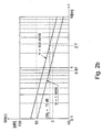
- 5b and 5c show the power P TS (r) which is received by a TAG as a function of the distance r from the transmitter.
- FIGS. 5b and 5c clearly show that the power P TS at a carrier frequency of, for example, 2442 MHz is significantly greater than that at a carrier frequency of 5800 MHz, based on a specific distance location.
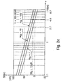
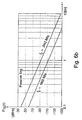
- FIGS. 6b and 6c shows in FIGS. 6b and 6c the power curve representation of the signal power P IS (r) which is received in the interrogation unit.
- the power in relation to a specific receiving location is significantly greater at the carrier frequency of 2442 MHz, for example, than at a carrier frequency of 5800 MHz.
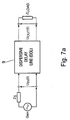
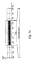
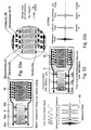
- FIG. 7 shows the block diagram of a dispersive converter device 9 (dispersive delay line DDL) in FIG. 7a.
- an input signal U IN (t) is generated by means of a generator (Gen) with the zero impedance Z S across the input terminals of the dispersive converter device.
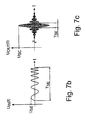
- the input signal U IN (t) is a chirp signal -Fig. 7b and 7d - more precisely, an up-chirped signal with an amplitude U SE of 1 V and a time duration T SE of one microsecond.
- the carrier frequency is 1000 MHz and the bandwidth of the chirp signal is approximately 100 MHz.
- the chirp signal shown is a linear frequency-modulated pulse of the duration T SE , within which the frequency changes from a lower to an upper frequency in a continuously linear manner (upchirp) or falling (downchirp).
- the difference between the upper and lower frequency represents the bandwidth B S of the chirp pulse.
- T SC denotes the time interval between the two zeros of the main maximum of U OUT (t).
- FIG. 7d shows the chirp signal according to FIG. 7b in a somewhat different representation.
- the chirp signal has a time length of one microsecond with a signal amplitude from 1V.
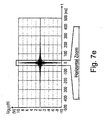
- Fig. 7e shows the output pulse signal of the DDL 9 (Fig. 7a) and shows the same Output pulse signal of the DDL stretched in time (horizontal zoom).
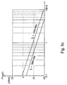
- 9a and 9b show the behavior of the signal noise factor SN (r), based on the distance r between the TAG and the interrogation unit, as a function of different expansion factors ⁇ and different interrogation cycles N R.
- DDL dispersive delay line
- IDT weighted interdigital transducer
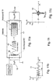
- the signal to excite the dispersive transducer is generated as follows:
- the sinx / x-shaped signal of the generator 10 and that in the carrier frequency generator 11 generated carrier frequency signal are the inputs of a four quadrant multiplier 12 fed. This already occurs at the output of the multiplier 12 prescribed pulse signal 13.
- this pulse signal 13 is given to the dispersive converter 9, then arise two surface waves 14, 15, which are on the substrate in opposite directions Spread the direction. Both surface waves have a complementary one to the other Chirp characteristic.
- a first surface wave 14 is shown in the image upchirp characteristic on the left and a second surface wave 15 with downchirp characteristic on the right side of the dispersive converter.
- 11 a shows an SAW converter arrangement in which a chirp signal U IN (T) 18 is initially applied to a non-dispersive converter 16. This then generates a corresponding "chirped" acoustic wave, which is received in a dispersive transducer 9, so that the already-described and known time-compressed pulse signal U OUT (T) according to FIG. 11 c is generated on the output side.
- the signal functions of the input signal and the output signal are shown in sub-figures 11b and 11c.
- FIG. 13a shows a similar arrangement to FIG. 12, but here two non-dispersive transducers 16 are arranged one behind the other, ie spatially staggered, on the side of the substrate opposite the dispersive transducer 9.
- two compressed pulse signals U OUT1 (t), U OUT2 (t) of the same signal profile - FIG. 13c - are produced on the output side, but because of the running time of acoustic wave on the substrate are offset from one another by the distance ⁇ T 21 .
- the time offset ⁇ T 21 should be at least equal to T SC , but the time offset ⁇ T 21 is preferably approximately three to ten times as large as the distance between the zeros of the main maximum of U OUT1 (t) and U OUT2 ( t).
- the time offset between the two pulsed output signals is required so that the interrogation unit can reliably detect and examine them when these signals are received.
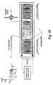
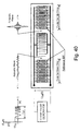
- FIG. 14 shows an SAW converter device in the illustration according to FIG. 14a a dispersive converter 9 and a non-dispersive converter device 20 from eight non-dispersive transducers 16.
- dispersive and non-dispersive converters are comparable.
- Both point a "positive" electrode 21 or 22 and a negative electrode 23 or 24.
- the electrodes have the free line ends 25 (fingers) to each other and the free line ends 25 are interleaved without touching each other.
- the positive electrodes of the non-dispersive transducers 16 are in Fig. 14a via a common bus line - hereinafter referred to as positive bus line - 26 connected.
- the negative electrodes 23 of the non-dispersive transducers 16 are in 14a connected to each other via a negative bus line 27.
- Fig. 14a What can be seen are dispersive transducers 9 and non-dispersive transducer devices 20 electrically isolated from each other, and their coupling is only acoustic Surface wave coupling.
- 14a are all non-dispersive transducers connected to the respective positive and negative bus lines in the same way. This means that it generates when excited with an SAW pulse signal from the dispersive converter 9 would react with a pulse train, each Pulse is offset in time from the previous one, but has the same shape. This comes from coding or programming eight logical ones "11111111" equal.
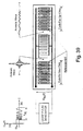
- the 14b shows the arrangement according to FIG. 14a, but now with a coded / programmed one non-dispersive transducer arrangement.
- the coding / programming consists in the specific example that the connecting line between the electrodes and the bus lines of the second, fifth and sixth Converter are removed or interrupted. With a suggestion with an SAW Pulse signal - generated by the dispersive converter 9 - can therefore these converters do not emit an electrical signal in the bus line, so that a pulse sequence results, which corresponds to a code "10110011".
- the distance or the interruption of existing electrode bus line connections is a first preferred The programming method.
- the removal or interruption of connecting lines between the positive and negative electrodes by any technology, advantageously by laser cutting or etching.
- FIG. 15 shows a further embodiment of the one already shown in FIG. 14b Surface wave transducer device in which the positive electrode 22 of the dispersive converter 9 electrically separated from the positive bus line 26. The same applies to the negative electrode 24 of the dispersive transducer and the negative bus line 27 of the non-dispersive converter.
- both the pair of electrodes of the dispersive converter and the bus lines of the An antenna (30 or 33) is assigned to each non-dispersive converter device.
- the antenna 33 consists of two parts 31 and 32, the first part 31 with the positive electrode and the second part 32 with the negative electrode of the dispersive Converter 9 is connected.
- the converter device reacts as already described on the output side with a pulse train in the logical meaning "10110011".
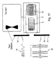
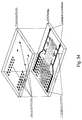
- This exemplary identification code was already based on Fig. 14 described. It can be seen that in the places where the second, fifth and sixth converter of the converter device 16 not with the positive and negative Bus lines is connected, also no pulse is generated, which is in the interrogator easy to read, determine and evaluate. You can also see that the Output signal is a signal with two logic states, namely the states "Pulse”, synonymous with logic "1” and the state "no pulse” synonymous with the logic state "0". 15 is an example above Identification "TAG-CARD” shown on which the SAW converter device is arranged and on which it can be seen that the two antenna arrangements - receiving antenna 30, transmitting antenna 33 - are arranged crossed on the map.
- FIG. 16 shows in FIG. 16c a surface wave converter device in which the positive electrode of the dispersive transducer 9 with the positive electrode of the non-dispersive Converter 16 and the negative electrode of the dispersive converter 9 with the negative electrode of the non-dispersive transducer 16 are connected.
- a chirp signal emitted by the pulse generator is then simultaneously above that dispersive transducer 9 as above the non-dispersive transducer 16.
- Compressed the dispersive converter 9 generates the chirp signal and generates a first pulse-shaped Surface wave in the direction - see also Fig. 16a - of the non-dispersive transducer, while at the same time the non-dispersive transducer is an opposite one generates second surface wave, which in the direction - see also Fig. 16b - des dispersive transducer spreads.
- This second surface wave has a received signal corresponding to a chirp-like characteristic.
- the first pulse-shaped SAW is also received when it arrives at the non-dispersive converter converted into a pulse-shaped electrical signal, while the second chirp-shaped SAW compressed on arrival at the dispersive transducer and also in one pulse-shaped electrical signal is converted, which is simultaneous and in phase with the electrical pulse signal of the non-dispersive transducer on the Bus lines of the electrodes occur.
- 16 therefore represents the proof symbolically shows that the arrangement according to 16a and 16b can be superposed, to get 16e.
- FIG. 17 shows an example of the structure of a TAG card with the arrangement presented in FIG. 16c, in which the electrodes of the dispersive converter are connected to the common bus lines 71 of the non-dispersive converter.
- the converter device shown reacts to an electromagnetic chirp signal 14 as an input signal with a pulse sequence 40, which has the logical meaning of a binary sequence of "10110011". It goes without saying that the number n of non-dispersive transducers 16 can easily be increased, for example to more than 30, and that this results in a large number of programming options, namely more than 2 30 .
- 18 shows a further alternative embodiment of the invention.
- the second to eighth non-dispersive converters with both their positive and also with its negative electrode to the negative and positive bus line at the same time connected.
- non-dispersive converter 37 is connected to the positive bus line and connected to the negative bus line with its negative electrode.
- This first converter element 37 serves - as will be explained later - as Reference element for the other non-dispersive converters.
- 18b shows the Structure from Fig.
- the second Transducer 38 which is closest to the reference element 37, with its negative Electrode only on the positive bus line and with its positive electrode is only connected to the negative bus line. All others originally existing Connections to a bus line are separated by the coding. The same applies to the fifth and sixth converters.
- the third, fourth, fifth and sixth transducers of the non-dispersive transducer arrangement are normal, ie with the positive electrode to the positive bus line and the negative electrode connected to the negative bus line.
- a TAG with a like in 18b shown converter structure with a chirp signal for example a
- the TAG system responds with a pulse train consisting of from 8 pulses.
- the first pulse - see Fig. 18c - is the reference pulse, generated by the reference element 37.
- All other pulses, those of non-dispersive Transformer elements originate that are just as positive and negative bus line are connected like the reference element, are in phase with the reference pulse.
- the however, generate second, fifth and sixth non-dispersive transducer elements due to their reverse connection to the positive and negative bus line pulse signals, which are not in phase with the reference pulse.
- Figure 18d shows this relationship, with a pulse which is "in phase” with the reference pulse is interpreted as "bit 1", and a pulse which is "out of phase” to Reference pulse is interpreted as "bit 0".
- FIG. 18e shows the structure arrangement of the positive once again in the enlargement and negative electrodes to the positive and negative bus lines in the reference element 37, an "out of phase” converter 38 and an “in phase” converter 39.
- the associated antenna 30 with its part is shown in FIG. 18b 31 and 32 not shown.
- 19 shows in a further advantageous embodiment a “quasi” interconnection of the structures, as has already been described with reference to FIGS. 17 and 18.
- 19a again shows the SAW converter device in the "uncoded / unprogrammed” state, in which the positive and negative electrodes of the non-dispersive converter are each connected to the positive and negative bus lines.
- 19b shows a coding in which individual, non-dispersive transducer arrangements are either connected to the bus line "in phase”, or are connected “out of phase” to the bus line or are not connected to the bus line at all. This is shown again in enlarged form in FIG. 19c. From left to right you can again see the reference element 37, the "out of phase” converter 38, the "in phase” converter 39, and the non-connected converter 40.
- FIG. 19d shows the interpretation of the pulse signals in the legend, which are generated by the various converters.
- Converter 37 again generates the reference pulse signal
- converter 38 a pulse signal that is out of phase with the reference pulse signal
- converter 39 a signal that is in phase with the reference pulse signal
- converter 40 does not generate a pulse signal because it is not is connected to the bus lines.
- the dispersive converter in turn provides a pulse signal to which the non-dispersive converter arrangement 16 responds with the pulse train 41.
- FIG. 20 shows a converter arrangement which is identical in terms of signal processing is like the surface wave converting device shown in Fig. 19. However are here the starting point before programming / coding the second to eighth (i.e. n-1) non-dispersive transducers with neither the positive nor the negative Bus line connected.
- Each electrode of the individual non-dispersive transducers has two connection points 73a, 73b, one connection point 73a of the positive 71 a and a connection point 73 b assigned to the negative bus line 71 b or is arranged adjacent to this.
- the same programming as for the one shown in Fig. 19 solution is now by the corresponding connection 72 of the connection electrodes manufactured with the desired bus lines.
- FIG. 20b 20c and 20c show the bonded connections 72 of the respective electrode connections to the bus line connections. It is obvious that with a bond every desired programming can be carried out very easily and that It is particularly advantageous that the basic structure of the converter device - see. FIG. 20a - is always the same. This enables inexpensive production.
- FIG. 21 shows an alternative way of connecting the electrode connections to FIG. 20 with the bus line connections of the non-dispersive converter 16.
- SAW structure surface wave transducer structure
- FIG. 21 shows an alternative way of connecting the electrode connections to FIG. 20 with the bus line connections of the non-dispersive converter 16.
- SAW structure surface wave transducer structure
- it can is a mass article that can be manufactured cheaply.
- an upper plate 43 for example, on the lower plate 42 a silicon chip 74.
- This upper plate already shows on its underside prefabricated "code defining" connections, so that only when the upper plate 43 on the lower plate 42 the desired connections the non-dispersive transformer to the positive and negative bus lines become.
- the production of "connecting plates” - like plate 43 - can be carried out very inexpensively.
- the two plates can be connected through the most diverse connection techniques, for example through Gluing, flip chip technology etc.
- connection techniques for example through Gluing, flip chip technology etc.
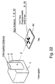
- the TAG 22 shows in a clear representation an identification system consisting of the interrogation unit 1 and a TAG 44 on which the SAW structures shown on the basis of the figures described are implemented.
- the TAG is programmable only once (OTP - one time programmable), for example by applying the plates - as shown in FIG. 21 - or by bonding - as shown in FIG. 20 - or by a Remove lines - as shown in FIG. 19. It was found that the maximum distance between the TAG and the interrogation unit 1 can still be 2.7 m at the permissible field strength H max of the interrogation unit, so that reliable interrogation communication is guaranteed. The query distance of 2.7 m was reached when the query unit emitted a chirp signal as the query signal.
- the query distance r was already 8.7 m in the comparison case.
- the interrogation distance r is already 18 m. It can easily be achieved with the TAGs that more than 10 9 different codes can be programmed with them, so that the identification system has a very large variability / capacity.
- FIG. 23 shows the arrangement of an identification system shown in FIG. 22, consisting of an interrogation unit 1 and a TAG 44.
- the tag 44 shown can be reprogrammed here (RP-re-programmable). This reprogramming can be achieved if - see also FIG. 19a - the positive and negative electrodes of the non-dispersive transducers 16 are each connected to the positive and negative bus lines at the same time.
- the connection pads do not use fixed connections, such as bonding wires, for example, but rather switch elements, which are preferably field effect transistors, which are connected to a circuit driver.
- the circuit driver controls the "open” or "closed” position of the switch transistors.
- the transistors can now be controlled in a simple circuit.
- the energy required for the operation of the circuit can be made available on the TAG with a battery 76, this battery preferably being a foil battery.
- each antenna has a main lobe 50 and thus only TAGs can identify those arranged at a certain spatial angle to the antenna are.
- the main lobes can be directed in the desired direction adjust what a very large selection of the query related to each geographic location of a TAG means. If a TAG is used by two antennas at the same time "queried", the exact geographical location of the Find TAGs.
- the interrogation unit is arranged in the garage of a house is.
- the TAG is arranged in the car, better still an integral part of the automobile, for example in the windshield, so that it is there cannot be removed easily.
- the distance at which the interrogation unit is reached at some point receives a TAG-encoded signal after the transmission of interrogation signals and this identifies. If the TAG code matches the code when evaluating, for which an evaluation unit of the interrogator is waiting Control of an automatic garage door operator opened the garage.
- the illustrated Solution is very advantageous also in hotel garages, so that the hotel guest after the Check in at the hotel there gets a TAG and drive his automobile into the garage can without having to get a conventional key.
- the TAG can also be the room key at the same time, if the room door via a corresponding interrogation unit and an opening mechanism, which is controlled by the interrogator. After checking out the guest 's identifier is set to "non valid" so that neither Then let the hotel door open the hotel garage. This system sets one simple data network ahead, which can be easily established.
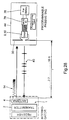
- Fig. 26 shows another application example. This is a common situation shown on a freeway with several vehicles below a signpost drive through. Two interrogation units sit on this signpost, left and right on the mast. As soon as the automobile approaches and into the area of the maximum distance, the interrogation unit can send back the message from the TAG Code signal - the TAG is in turn in the car, on the car or an integral part of the car, for example the windshield - process and to one send central data unit.
- the surface wave transducer device according to the invention, thus the TAG according to the invention applies to all possible products can be attached, be it as a card, be it as adhesive film or the like.
- the TAG is an integral part of the Products is what is given even if it is glued to the product or is permanently connected to it in any other way.
- TAGs shows an overview of the mode of operation and structure of the invention TAGs, with the TAG only programmable once in the example shown is.
- the still reasonable distance between the TAG and the query unit mainly depends on the number of queries also from the interrogation signal, which is advantageously a chirp signal, but can also be another radio frequency pulse.
- the TAG sends back a pulse train whose Amplitude and / or phase from the programming of the non-dispersive transducers depends.
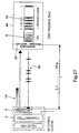
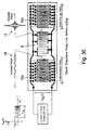
- Fig. 28 The structure of an identification system according to the invention with one according to the invention Re-programmable TAG is shown in Fig. 28.
- the SAW filter structure 9, 16 is connected to a MOS IC 78 with which the transistors, those in the connecting line between the positive electrodes and the Bus lines of the non-dispersive converter are switched.
- the programming can be changed at any time.
- For energy supply is e.g. a foil battery 76 (pre-charged capacity, solar cell, etc.) provided so that the reprogrammable TAG 44 over a long as possible Lifetime.
- the battery can also be used Preset the permissibility of such TAGs, for example in card systems is advantageous so that a card with a TAG according to the invention only for a certain time is valid. For this purpose, it is advantageous if the TAG also has a time switch.
- TAG 29 shows the production of a TAG according to the invention, this consisting of three Layers 79, 80 and 81, and the first and third layers 79, 81 one Represent protective layer and the middle layer 80 is formed from a spacer film is within which the surface wave transducer structure according to the invention (SAW) is arranged together with the antenna and the foil battery.
- SAW surface wave transducer structure according to the invention
- FIG. 30 shows various options for connecting a SAW (Surface Acoustic Waves) chips and a silicon connection chip, whereby on the Silicon connection chip the respective connections are arranged so that a Programming / coding of the SAW is guaranteed.
- the connection can be done once as shown by bonding - Fig. 30a - or by a so-called Flip chip technology - see p. Fig. 30b - in which the silicon connection chip on the SAW chip similar to how it works in flip chip technology. It is also possible, to arrange the SAW structure above the silicon connection structure - Fig. 30c - or the SAW structure and the respective connections in one production process to be provided on a silicon wafer.
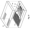
- FIG. 31 shows the connection between an SAW circuit 83 and a silicon chip 82, with the SAW structure on the bottom plate 42 and the silicon chip on the upper plate 43 is arranged.
- the lower plate 42 with the SAW structure faces Mains connection areas 51 and 52 and programming connection connections 53.
- the upper plate which only partially covers the lower plate, so that a part of the Mains voltage connections 51 and 52 remains uncovered, also has programming connection connections 54 and network connection connections 55.
- the top plate has a silicon chip 82, the structure of which is still shown in FIG. 45 is explained in more detail.
- both the associated program connections are located 53 and 54 as well as the mains voltage connections 51, 52 and 55 one above the other, with part of the mains voltage connections 51 and 52 from the plate remains uncovered. It would be very easy now to have an appropriate power supply, which is applied to the mains voltage connections and a corresponding one Programming via the antenna connections 57 and the silicon chip 82 to program the SAW structure, i.e. TAG 44. This is reprogramming anytime possible.
- the dispersive transducer 9 receives a chirp pulse generated by a chirp pulse generator, then it generates two surface acoustic waves, namely a compressed surface wave pulse signal 13 and an expanded chirp pulse 58. that the compressed pulse 1 moves to the left and the expanded chirp pulse signal to the right (in the drawing).
- the respective signals meet a non-dispersive converter device, so that the signals U COM (t) and U EXP (t) are generated on the output side as electrical signals.
- the respective signal form of the compressed as well as the expanded signal are shown in FIGS. 32b and 32c.
- Such an arrangement has the advantage of sending up-chirps and subsequently down-chirps from the interrogation unit in order to increase the program capacity or to switch to different interrogation hierarchies.
- the dispersive transducer 9 is made in several parts, in the example shown it consists of three parts 84a, 84b, 84c, the first part being suitable for high-frequency Signals, the second part is suitable for medium-frequency signals and the third Part is able to process low-frequency signals and corresponding To generate surface wave signals.
- Fig. 33a shows that the three parts of the dispersive transducer 9 unconnected to the respective positive and negative Bus line are arranged connected.
- the respective positive and negative Electrodes of the respective dispersive transducer parts have pads that are located adjacent to the negative and positive bus lines.
- the dispersive converter device 9 is also programmable, which is the total programming or coding capacity of the system elevated.
- the TAG shown in FIG. 33b must therefore be excited with a chirp signal be, the frequency bandwidth to the bandwidth of the high-frequency and medium-frequency dispersive transducer part is matched. With another programming the dispersive transducer device would have to use a different interrogation signal are responded to the query signal with a TAG signal can be.
- FIG. 34 shows the programming of the TAG already described in FIG a programmable dispersive converter device, the programming by placing an upper plate on the lower plate, which is already based on 33a has been explained.
- the top plate points according to the programming desired connection surfaces on the respective connection contacts the positive and negative electrodes of the dispersive and non-dispersive Converter fit.
- 35 shows another alternative embodiment of the invention.
- a non-dispersive transducer device 16a and 16b is arranged. Any of these Converter devices 16a, 16b can be programmed with a different code.
- the dispersive converter device generates when a chirp signal is received, a time-compressed pulse signal and an expanded chirp pulse signal.
- the time-compressed migrates Pulse signal to the left and the expanded chirp pulse signal to the right Page.
- a pulse train is only from the non-dispersive Converter device generated to the left of the dispersive converter device if that TAG is excited with a down-chirp signal.
- the coding of the pulse sequence by the converter device 16 is on the right determined by the dispersive transducer device 9. Hence a certain one Code through the up-chirp signal and another code through the down-chirp signal certainly.
- FIG. 35 The structure complementary to FIG. 35 for the up-chirp and down-chirp signal shows Fig. 36.
- Figs. 37 and 38 show the structure similar to Figs. 35 and 36 with a programmable one dispersive transducer device 9 and arranged on both sides thereof non-dispersive converter device 16.
- the TAG is not programmed or is in this state programming.
- the programming can, as already explained with reference to FIG. 14, by cutting or removing certain connecting lines between the electrodes and the respective bus lines 71a, 71b.
- FIG. 39 and 40 show the arrangement of a "one-piece" dispersive Transducer device 9, each of which is in turn a non-dispersive one Converter device 16 is included, both of which are non-dispersive converter devices are programmable differently.
- Fig. 39 shows the arrangement for a down-chirp pulse as an interrogation signal
- Fig. 40 shows the case for an up-chirp pulse as an interrogation signal. Programming can in turn be done by removing the connecting line.
- FIGS. 41 b and 41 c show the pulse signal sequence when excited with a down-chirp signal and an up-chirp signal.
- the code for the down-chirp signal is here by the Letter string "RBACBBCA” and the code for the up-chirp signal is through the sequence of letters "RCBACBAB”.
- the programming required for this can be seen directly from Fig. 41.
- the respective pulse signal sequences for the The down-chirp signal and the up-chirp signal as an interrogation signal are shown in FIGS. 41 b and 41 c shown.
- the signal sequence of the compressed pulses is overlaid by the expanded chirp signal, but that the amplitude of the expanded chirp signal far below the maximum amplitudes of the time-compressed Pulse lies and therefore a sufficiently good distinction between the time-compressed pulse signals and the expanded chirp signal is possible.
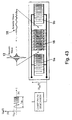
- FIG. 42 shows another alternative embodiment of the invention.
- two dispersive transducer devices arranged on the TAG, the one non-dispersive Include converter device.
- the first dispersive converter device 9a When excited with a down-chirp pulse signal the first dispersive converter device 9a generates an expanded one Chirp pulse signal and the second dispersive converter device 9b a time-compressed Pulse signal.
- the complementary case is shown in Fig. 43, so that with the up-chirp pulse signal as the interrogation signal, the first converter device 9a time-compressed pulse signal and the second dispersive converter device 9b expanded chirp signal generated.
- Fig. 44 shows the signal structure of the SAW structure shown in Figs. 42 and 43 Excitation with an up-chirp signal and with excitation with a down-chirp signal.
- the respective pulse code sequences 40 for the up and Down-chirp signal are reciprocal to each other, so that an interrogation unit at the staggered generation of an up-chirp and down-chirp signal the reciprocal Pulse signal sequences can check for their (reciprocal) agreement leads to increased query security and only allows acceptable results, if the TAG is structured as shown. So the TAG is missing, for example the second dispersive converter device, the interrogation unit would received no pulse signal sequence on the down-chirp signal, and possibly evaluate the evaluation with "non-valid".
- the TAG has the OFW (SAW) structure 60 already described, an antenna device 61 and a silicon chip 62.
- the silicon chip has a switching matrix 63, a microcontroller 64, a reprogrammable memory 65, a programmable one Interface 66 and a low-pass filter 67.
- the Silicon chip via a connection to a power supply 68, for example a battery, a solar cell, a charge capacity, etc.
- the low-pass filter 67 is connected to the antenna parts of the antenna 61.
- the SAW structure is also 60 connected to the switching matrix 63, which in turn is connected to the microcontroller 64 is connected, which is connected to the memory 65 and the interface 66 is.
- FIG. 46 A further embodiment of the TAG according to FIG. 45 is shown in FIG. 46.
- the microcontroller here has a further interface to a data source 69 on, which in the example shown is formed by a sensor, above the data, preferably programming data - e.g. Temperature, environmental data, biometric Data (e.g. fingerprint) - can be entered into the microcontroller, so that the SAW structure can be programmed accordingly.
- programming data - e.g. Temperature, environmental data, biometric Data (e.g. fingerprint) - can be entered into the microcontroller, so that the SAW structure can be programmed accordingly.
- biometric Data e.g. fingerprint
- Fig. 47 The principle of programming is shown in Fig. 47.
- the programming device 90 can in turn be connected to an external device, for example a Computer, a network, etc. are in data connection.
- an external device for example a Computer, a network, etc.
- the different codes can be selected.
- the programming of the re-programmable TAG is in the system display 48 further explained. It can be seen here that the TAG into a Programming device 90 is introduced in which a single identification code or a plurality of identification codes are loaded into the code memory of the TAG become.
- the programming data is transmitted in the low-frequency frequency band, so that they can be detected by the low-pass filter.
- the data preparation of the Programming data takes place in the programming interface.
- Fig. 48 it can be seen that the Antennas 91, 92 of the programmer 90 are arranged very close to the TAG antennas, thus the high transmission energy required for programming can be made available.
- the TAG is on a measuring device, e.g. Environmental data measuring device, arranged, it is expedient for measurement data to be transmitted to the TAG via a data input be, so that the TAG a pulse code sequence with a corresponding query sends out, which represents the respective measurement signal. So it is with simplest means possible to wirelessly query measuring signals from a measuring device, without the measuring device having its own active transmitter. By a corresponding control of the data input, whole measurement signal sequences can also transmitted to the interrogation unit when the TAG is queried accordingly become.
- a measuring device e.g. Environmental data measuring device
- each measurement signal contains a specific identification code, which the respective TAG and thus the corresponding measuring device identified.
- the other coded Data then represent the desired measurement signal to be queried.
- the TAG can measure with any other possible data source be coupled, which transmits data to the TAG, which in turn from the Interrogator can be queried.
- a data source can also be a medical-technical one Device or a data processing device.
- the interrogator already has an identifying pulse sequence transmits, to which only one TAG, which is programmed as it is the identification pulse sequence corresponds, reacts with a desired response signal. Consequently it is possible to include the presence of certain ident tags too selectively determined by other TAGs.
- the interrogator first sends a chirp signal and followed by an identification pulse sequence, so that for the TAG sought very reliable query can be made.
- IDT inter-digital converters
- the layout of the metal electrodes of the SHW filters can be many different Types are made (e.g. split finger technology), the ones shown Realizations only describe the principle of operation.
- the geometrical arrangement of the transducers not due to linear expansion of the SAW limited.
- the SAW could do well reflective reflectors are deflected. The resulting loss of reflection is low because maximum reflection is easy due to periodic structures can be achieved.
- the signals are compressed by the reflector structure having a chirp characteristic having.
- the dispersive IDT it is also possible to use the dispersive IDT to be realized by a linear IDT, followed by a dispersive reflector is, so that this compresses the SAW and on the coded arrangement of the reflected non-dispersive IDT.
Landscapes
- Engineering & Computer Science (AREA)
- Physics & Mathematics (AREA)
- Signal Processing (AREA)
- Acoustics & Sound (AREA)
- Computer Networks & Wireless Communication (AREA)
- General Physics & Mathematics (AREA)
- Theoretical Computer Science (AREA)
- Radar Systems Or Details Thereof (AREA)
- Surface Acoustic Wave Elements And Circuit Networks Thereof (AREA)
- Control Of High-Frequency Heating Circuits (AREA)
- Near-Field Transmission Systems (AREA)
- Amplifiers (AREA)
- Transducers For Ultrasonic Waves (AREA)
- Burglar Alarm Systems (AREA)
- Road Signs Or Road Markings (AREA)
Claims (46)
- Dispositif transducteur à ondes de surface, comprenant la combinaison d'un premier dispositif de transmission (9) du type dispersif et d'un second dispositif de transmission du type non dispersif, ce dernier se composant d'une pluralité de transducteurs (16) non dispersifs, qui sont codés avec un code d'identification, les espacements respectifs de transducteurs voisins non dispersifs étant identiques et la contribution d'un seul transducteur au code étant déterminée par une liaison aux électrodes du transducteur et la polarité avec laquelle il se fait.
- Dispositif transducteur à ondes de surface selon la revendication 1,
caractérisé en ce que les n transducteurs (16) non dispersifs sont programmés/codés et/ou commutés de telle sorte que, en cas d'excitation avec un signal, ils émettent un signal identifiant le dispositif transducteur à ondes de surface. - Dispositif transducteur à ondes de surface selon l'une quelconque des revendications-précédentes,
caractérisé en ce que chaque transducteur non dispersif présente une électrode positive et une électrode négative et en ce qu'une ligne de bus positive est attribuée localement à l'électrode positive des n transducteurs et une ligne de bus négative est attribuée localement à l'électrode négative des n transducteurs et en ce que le codage/l'identification souhaité du dispositif transducteur à ondes de surface est effectué par le choix de la liaison entre les électrodes de transducteur positives et négatives et les lignes de bus positives et négatives. - Dispositif transducteur à ondes de surface selon l'une quelconque des revendications précédentes, le dispositif réagissant à un signal d'entrée électromagnétique avec un signal de sortie et le signal de sortie étant conçu de telle sorte qu'il présente au moins trois états (ABC) logiques différents.
- Dispositif transducteur à ondes de surface selon l'une quelconque des revendications précédentes,
caractérisé en ce que, lors de la réception d'un signal Chirp, le dispositif génère un grand nombre d'impulsions qui sont émises de façon successive dans le temps sous la forme de signaux de sortie. - Dispositif transducteur à ondes de surface selon l'une quelconque des revendications précédentes,
caractérisé en ce que le dispositif émet successivement m signaux d'impulsion en cas de réception d'un signal Chirp, où n ≥ m et m correspond au nombre des transducteurs non dispersifs qui ne fournissent pas de signal d'impulsion. - Dispositif transducteur à ondes de surface selon l'une quelconque des revendications précédentes,
caractérisé en ce que l'électrode positive du dispositif de transmission du type dispersif est reliée à la ligne de bus positive et l'électrode négative du transducteur du type dispersif est reliée à la ligne de bus négative. - Dispositif transducteur à ondes de surface selon l'une quelconque des revendications précédentes,
caractérisé en ce que le dispositif présente un système d'antenne comprenant deux parties, la première partie de l'antenne étant reliée à la ligne de bus positive et l'autre partie à la ligne de bus négative. - Dispositif transducteur à ondes de surface selon l'une quelconque des revendications précédentes,
caractérisé en ce que tous les transducteurs sont branchés électriquement en parallèle au moyen d'un circuit de programmation. - Dispositif transducteur à ondes de surface selon l'une quelconque des revendications précédentes,
caractérisé en ce qu'au moins l'un des n transducteurs non dispersifs sert d'élément de référence. - Dispositif transducteur à ondes de surface selon l'une quelconque des revendications précédentes,
caractérisé en ce que des transducteurs (16) du type non dispersif sont disposés seulement sur un côté ou sur les deux côtés du dispositif transducteur (9) du type dispersif. - Dispositif transducteur à ondes de surface selon l'une quelconque des revendications précédentes,
caractérisé en ce que, en cas de réception d'un signal d'entrée, qui est une courte impulsion de radiofréquence, ce signal est transformé par le système de transmission dispersif en une première onde de surface de forme Chirp, qui se propage en direction des n transducteurs non dispersifs et déclenche des impulsions électriques de Chirp lors du passage des transducteurs non dispersifs, impulsions dont la superposition sur les lignes de bus représente le code programmé, alors qu'au cours de la même période les transducteurs non dispersifs et également excités par le signal d'entrée génèrent une succession d'ondes de surface représentant le code programmé, dont la caractéristique est identique à celle du signal d'entrée et qui se propagent en direction du système de transmission dispersif, où elles sont converties en impulsions électriques avec une caractéristique en forme de Chirp, qui sont émises simultanément et de façon précise en phase avec les impulsions de Chirp, générées par la première onde de surface, des transducteurs non dispersifs. - Dispositif transducteur à ondes de surface selon l'une quelconque des revendications précédentes,
caractérisé en ce que le système de transmission génère des signaux qui peuvent encore être bien reçus même à une distance (r) de plus de 2 mètres. - Dispositif transducteur à ondes de surface selon l'une quelconque des revendications précédentes,
caractérisé en ce qu'un signal de Chirp présente comme signal d'entrée une longueur dans le temps de 0,5 à 1,5 µs, de préférence 1 µs et en ce que le signal de Chirp présente une largeur de bande de fréquence de 50 jusqu'à 250 MHz. - Dispositif transducteur à ondes de surface selon l'une quelconque des revendications précédentes,
caractérisé en ce qu'un signal d'impulsion, qui est généré par le dispositif transducteur du type dispersif en cas de réception d'un signal de Chirp, présente sensiblement une durée d'impulsion principale (Tsc), qui est calculée selon l'équation suivante : - Dispositif transducteur à ondes de surface selon l'une quelconque des revendications précédentes,
caractérisé en ce que l'intervalle de temps de signaux d'impulsion successifs du second dispositif transducteur du type non dispersif est au moins aussi grand que la durée dans le temps (Tsc) du signal d'impulsion. - Dispositif transducteur à ondes de surface selon la revendication 16, caractérisé en ce que l'intervalle représente plusieurs fois, en particulier cinq à dix fois, la durée d'une seule impulsion.
- Dispositif transducteur à ondes de surface selon l'une quelconque des revendications précédentes,
caractérisé en ce que les premier et second dispositifs transducteurs (9, 16) sont des transducteurs interdigitaux (IDT). - Dispositif transducteur à ondes de surface selon l'une quelconque des revendications précédentes,
caractérisé en ce que les transducteurs non dispersifs (16) réagissent à un signal d'impulsion avec un signal d'impulsion à deux phases, la position de phase du signal d'impulsion individuel dépendant préférentiellement du fait que l'électrode positive ou l'électrode négative du transducteur (16) concerné est raccordée à la ligne de bus positive ou négative. - Dispositif transducteur à ondes de surface selon l'une quelconque des revendications précédentes,
caractérisé en ce que tous les transducteurs (16) non dispersifs commutés de façon active sont raccordés avec l'électrode positive à la ligne de bus positive et avec l'électrode négative à la ligne de bus négative. - Dispositif transducteur à ondes de surface selon l'une quelconque des revendications précédentes,
caractérisé en ce que le dispositif transducteur du type non dispersif présente des transducteurs (16) qui, en cas d'excitation avec un signal, génèrent soit un signal qui est en phase (in-phase) avec le signal d'excitation, soit un signal qui n'est pas en phase (déphasé-off) avec le signal d'excitation ou ne génèrent pas de signal. - Dispositif transducteur à ondes de surface selon l'une quelconque des revendications précédentes,
caractérisé en ce que la programmation/le codage des transducteurs du type non dispersif s'effectuent par le fait qu'à chaque fois des lignes de liaison souhaitées allant du bus positif ou négatif aux électrodes positives et/ou négatives des transducteurs sont prévues, les lignes de liaison étant de préférence bondérisées. - Dispositif transducteur à ondes de surface selon l'une quelconque des revendications précédentes,
caractérisé en ce que la programmation/le codage des transducteurs du type non dispersif sont déterminés par le fait que des lignes, qui existent d'une part entre la ligne de bus positive et l'électrode positive et l'électrode négative des transducteurs et d'autre part entre la ligne de bus négative et les électrodes positives et négatives des transducteurs, sont séparés en fonction du codage souhaité. - Dispositif transducteur à ondes de surface selon l'une quelconque des revendications précédentes,
caractérisé en ce que chaque électrode d'un transducteur (16) du type non dispersif présente un premier raccordement et un deuxième raccordement et en ce que le premier raccordement est disposé à proximité de la ligne de bus négative et le deuxième raccordement à proximité de la ligne de bus négative. - Dispositif transducteur à ondes de surface selon la revendication 24,
caractérisé en ce que la programmation/le codage des transducteurs non dispersifs sont réalisés par le fait que des transducteurs non dispersifs sont disposés sur une plaque inférieure sans être reliés aux lignes de bus respectives et en ce que sur la plaque inférieure est disposée une plaque supérieure sur le côté, attribuée à la plaque inférieure, de laquelle sont disposées des lignes de liaison qui relient de la façon souhaitée les électrodes positives/négatives à la ligne de bus positive ou négative. - Dispositif transducteur à ondes de surface selon l'une quelconque des revendications précédentes,
caractérisé en ce qu'au moins l'un des transducteurs du type non dispersif présente des lignes de signalisation qui relient l'électrode positive et l'électrode négative aux deux lignes de bus et en ce que des interrupteurs sont disposés dans le cheminement du signal des lignes de liaison, les interrupteurs étant de préférence des transistors. - Dispositif transducteur à ondes de surface selon la revendication 26,
caractérisé en ce que le dispositif présente un module de commande de circuit avec mémoire pour la commande du circuit et un dispositif d'alimentation d'énergie, par exemple une batterie pour l'alimentation du module de commande de circuit et/ou des interrupteurs en énergie. - Dispositif transducteur à ondes de surface selon l'une quelconque des revendications précédentes,
caractérisé en ce que le dispositif transducteur est intégré dans une carte, qui comprend essentiellement trois couches disposées l'une sur l'autre, la première couche et la troisième couche représentant une couche de protection, entre laquelle se trouve la deuxième couche, à l'intérieur de laquelle sont disposés le premier et le second dispositifs transducteurs (9, 16) et l'antenne (30). - Dispositif transducteur à ondes de surface selon l'une quelconque des revendications précédentes,
caractérisé en ce qu'un premier ensemble de p transducteurs (16) non dispersifs est disposé sur un côté du dispositif de transmission du type dispersif et un second ensemble q de transducteurs (16) non dispersifs est disposé sur l'autre côté, en ce que le premier ensemble de p transducteurs est programmé avec un code 1 et le second ensemble de q transducteurs avec un code 2 et en ce que les codes sont de préférence différents les uns des autres. - Dispositif transducteur à ondes de surface selon l'une quelconque des revendications précédentes,
caractérisé en ce que le dispositif de transmission du type dispersif présente une longueur programmable. - Dispositif transducteur à ondes de surface selon l'une quelconque des revendications précédentes,
caractérisé en ce que le dispositif est conçu sur un substrat de silicium. - Dispositif transducteur à ondes de surface selon l'une quelconque des revendications précédentes,
caractérisé en ce que celui des n transducteurs non dispersifs qui est le plus proche du dispositif transducteur dispersif constitue un transducteur de référence (élément de référence), dont le signal (d'impulsion) est émis d'abord comme réaction à un signal (d'impulsion) du dispositif transducteur dispersif. - Dispositif transducteur à ondes de surface selon l'une quelconque des revendications précédentes,
caractérisé en ce que le nombre n des transducteurs (16) non dispersifs est supérieur à 30. - Dispositif transducteur à ondes de surface selon l'une quelconque des revendications précédentes,
caractérisé en ce que, sur les n transducteurs non dispersifs, n-k transducteurs sont programmables ou programmés, k étant inférieur ou égal à n. - Dispositif transducteur à ondes de surface selon l'une quelconque des revendications précédentes,
caractérisé en ce que le TAG est programmable une fois ou plusieurs fois. - Dispositif transducteur à ondes de surface selon la revendication 35,
caractérisé en ce que le dispositif présente un système de commande (64) pour la reprogrammabilité, qui est relié à une matrice de commutation (63), et présente une interface de programme (66) et un dispositif de mémoire, qui peut stocker un ou plusieurs codes d'identification ou une succession de données souhaitée, et en ce que le dispositif transducteur à ondes de surface est programmable à l'aide des données mémorisées. - Utilisation selon l'une quelconque des revendications précédentes pour l'identification de marchandises, de personnes ou d'animaux.
- Utilisation selon la revendication 37,
caractérisée par une unité d'interrogation/analyse (1)(interrogateur). - Utilisation selon la revendication 38,
caractérisée en ce que l'interrogateur (1) envoie un signal d'interrogation et reçoit et analyse un signal de réponse envoyé par le dispositif transducteur à ondes de surface. - Utilisation selon la revendication 38 ou 39,
caractérisée en ce que l'interrogateur (1) contient dans la partie d'émission et/ou de réception un niveau avec une caractéristique complémentaire du dispositif de transmission (9) dispersif. - Utilisation selon la revendication 38, 39 ou 40,
caractérisée en ce que l'interrogateur (1) est relié à un dispositif de traitement de données et/ou un système/réseau de traitement de données et envoie des repères d'identification (codes) reçus sur sa sortie. - Utilisation selon l'une quelconque des revendications 38 à 41,
caractérisée en ce que l'interrogateur présente des moyens pour la discrimination de phase. - Utilisation selon l'une quelconque des revendications 38 à 42,
caractérisée en ce que l'interrogateur présente des moyens pour l'émission d'un signal d'interrogation, le signal d'interrogation étant de préférence un signal Chirp ou une impulsion de radiofréquence. - Utilisation selon l'une quelconque des revendications 38 à 43,
caractérisée en ce que l'unité de réception de l'interrogateur (1) contient un niveau avec une caractéristique identique par rapport au dispositif transducteur dispersif et un autre niveau avec une caractéristique inversée en conséquence. - Utilisation selon la revendication 44,
caractérisée en ce que le dispositif transducteur à ondes de surface présente sur le côté du dispositif transducteur (9) dispersif un premier ensemble de p transducteurs (16) non dispersifs et sur l'autre côté un second ensemble de q transducteurs (16) non dispersifs, les électrodes du dispositif transducteur dispersif étant reliées à l'antenne et aux lignes de bus du transducteur non dispersif, le second ensemble de p transducteurs étant programmé avec un code 1 et le second ensemble de q transducteurs avec un code 2, en ce que le signal d'interrogation de l'interrogateur est une brève impulsion de radiofréquence et l'unité de réception d'un interrogateur (1) contient un niveau avec une caractéristique identique par rapport au transducteur dispersif et un autre niveau avec une caractéristique inversée en conséquence, de sorte qu'un signal d'interrogation émis par l'interrogateur et reçu par l'antenne est transformé par le transducteur dispersif en deux ondes de surface en forme de Chirp, se propageant dans le sens opposé, de caractéristique complémentaire (up-chirp, down-chirp), qui déclenchent à chaque fois un signal de code de codage différent et également avec une caractéristique de Chirp différente lorsqu'on atteint le premier ou le second ensemble de p ou q transducteurs, de sorte que les deux ensembles de transducteurs non dispersifs envoient en réaction au signal d'interrogation respectivement une série guidant le code concerné d'ondes de surface (SAW) en direction du transducteur dispersif, qui sont transformées à cet endroit en signaux de code avec une caractéristique de Chirp différente, de sorte qu'il se forme sur les lignes de bus communes un signal guidant les deux codes, composé d'impulsions up-Chirp, qui représentent le premier code, et d'impulsions down-Chirp qui représentent le second code, et en ce que le signal se formant sur les lignes de bus est transmis par l'antenne à l'unité de réception de l'interrogateur et est transformé ici par les niveaux dispersifs présentant une caractéristique complémentaire en une première succession représentant le code 1 et/ou une seconde succession représentant le code 2 d'impulsions de radiofréquence. - Utilisation d'un dispositif transducteur à ondes de surface selon l'une quelconque des revendications 1 à 36,
caractérisée en ce que le dispositif est couplé avec une source de données et transmet au dispositif des données qui peuvent être interrogées par une unité d'interrogation.
Priority Applications (1)
| Application Number | Priority Date | Filing Date | Title |
|---|---|---|---|
| EP03027970A EP1411463A2 (fr) | 1999-03-15 | 1999-04-01 | Transducteur à ondes acoustiques de surface et système d'identification équipé de ce dernier |
Applications Claiming Priority (3)
| Application Number | Priority Date | Filing Date | Title |
|---|---|---|---|
| DE19911369A DE19911369C2 (de) | 1999-03-15 | 1999-03-15 | Oberflächen-Wellen-Wandler-Einrichtung sowie Identifikationssystem hiermit |
| DE19911369 | 1999-03-15 | ||
| PCT/EP1999/002288 WO2000055806A1 (fr) | 1999-03-15 | 1999-04-01 | Transducteur a ondes acoustiques de surface et systeme d'identification equipe de ce dernier |
Related Child Applications (1)
| Application Number | Title | Priority Date | Filing Date |
|---|---|---|---|
| EP03027970A Division EP1411463A2 (fr) | 1999-03-15 | 1999-04-01 | Transducteur à ondes acoustiques de surface et système d'identification équipé de ce dernier |
Publications (2)
| Publication Number | Publication Date |
|---|---|
| EP1163632A1 EP1163632A1 (fr) | 2001-12-19 |
| EP1163632B1 true EP1163632B1 (fr) | 2003-12-10 |
Family
ID=7900957
Family Applications (2)
| Application Number | Title | Priority Date | Filing Date |
|---|---|---|---|
| EP99915736A Expired - Lifetime EP1163632B1 (fr) | 1999-03-15 | 1999-04-01 | Transducteur a ondes acoustiques de surface et systeme d'identification equipe de ce dernier |
| EP03027970A Pending EP1411463A2 (fr) | 1999-03-15 | 1999-04-01 | Transducteur à ondes acoustiques de surface et système d'identification équipé de ce dernier |
Family Applications After (1)
| Application Number | Title | Priority Date | Filing Date |
|---|---|---|---|
| EP03027970A Pending EP1411463A2 (fr) | 1999-03-15 | 1999-04-01 | Transducteur à ondes acoustiques de surface et système d'identification équipé de ce dernier |
Country Status (10)
| Country | Link |
|---|---|
| US (1) | US6788204B1 (fr) |
| EP (2) | EP1163632B1 (fr) |
| JP (1) | JP4061026B2 (fr) |
| KR (1) | KR20020006523A (fr) |
| CN (1) | CN100418104C (fr) |
| AT (1) | ATE256318T1 (fr) |
| AU (1) | AU3419899A (fr) |
| DE (2) | DE19911369C2 (fr) |
| DK (1) | DK1163632T3 (fr) |
| WO (1) | WO2000055806A1 (fr) |
Families Citing this family (37)
| Publication number | Priority date | Publication date | Assignee | Title |
|---|---|---|---|---|
| US6825794B2 (en) * | 2000-06-02 | 2004-11-30 | Research In Motion Limited | Wireless communication system using surface acoustic wave (SAW) second harmonic techniques |
| GB0102882D0 (en) * | 2001-02-06 | 2001-03-21 | Koninkl Philips Electronics Nv | Signalling system and a transport for use in the system |
| JP4007932B2 (ja) * | 2002-03-19 | 2007-11-14 | 株式会社タキオン | マイクロ波送電法、マイクロ波受電装置及びidタグシステム |
| JP3983692B2 (ja) * | 2002-03-19 | 2007-09-26 | 株式会社タキオン | マイクロ波送電装置、マイクロ波受電装置、マイクロ波送電法及びマイクロ波送電システム |
| US6756880B2 (en) * | 2002-03-21 | 2004-06-29 | Rf Saw Component Incorporated | Reader and response control system for discrimination between multiple surface acoustic wave identification tags and method of operation thereof |
| US6958696B2 (en) * | 2002-10-09 | 2005-10-25 | Rf Saw Components, Inc. | Transfer function system for determining an identifier on a surface acoustic wave identification tag and method of operating the same |
| US6759789B2 (en) * | 2002-10-18 | 2004-07-06 | Rf Saw Components, Inc. | Surface acoustic wave identification tag having an interdigital transducer adapted for code discrimination and methods of operation and manufacture thereof |
| US6922146B2 (en) * | 2003-04-24 | 2005-07-26 | Inksure Rf Inc. | Radio frequency data carrier and system for reading data stored therein |
| WO2006006768A1 (fr) * | 2004-07-14 | 2006-01-19 | Rnl Life Science Ltd. | Composition pour favoriser la croissance d'un animal comprenant des extraits d'artemisia capillaris thunberg, d'acanthopanax et d'ail et composition alimentaire pour favoriser la croissance comprenant cette composition |
| US7656296B2 (en) * | 2005-05-13 | 2010-02-02 | Ems Technologies, Inc. | Antenna for mobile wireless data collection system |
| US7548166B2 (en) * | 2005-05-13 | 2009-06-16 | Ems Technologies, Inc. | Tine-mounted antenna for an RFID |
| WO2006130988A1 (fr) * | 2005-06-10 | 2006-12-14 | Telecommunications Research Laboratories | Systeme de radiocommunications |
| US20070046438A1 (en) * | 2005-08-29 | 2007-03-01 | Mark Pempsell | Electronic Radio Frequency Identification Transceiver Device Activated by Radiant Means |
| US7616127B2 (en) * | 2005-11-03 | 2009-11-10 | Ems Technologies, Inc. | Removable mount for mounting an electronic system component on a forklift |
| US8565070B2 (en) | 2005-11-23 | 2013-10-22 | Cisco Technology, Inc. | System and method for active geographic redundancy |
| KR100775763B1 (ko) * | 2006-03-21 | 2007-11-09 | 엘지전자 주식회사 | Rfid 태그 및 그 제조방법 |
| KR100833550B1 (ko) * | 2006-11-07 | 2008-05-29 | 인하대학교 산학협력단 | 셀룰로오스 종이를 기재로 사용한 표면탄성파 기반의칩레스 수동형 전파식별 태그 및 셀룰로오스 종이 제조방법 |
| DE102007028289B4 (de) * | 2007-06-20 | 2010-07-29 | Epcos Ag | Mit akustischen Wellen arbeitendes elektrisches Bauelement mit einem RFID-Tag |
| US7633206B2 (en) * | 2007-07-26 | 2009-12-15 | Delaware Capital Formation, Inc. | Reflective and slanted array channelized sensor arrays |
| US20090072660A1 (en) * | 2007-09-19 | 2009-03-19 | Seagate Technology Llc | Slider That Utilizes Surface Acoustic Waves |
| US8342027B2 (en) | 2007-12-07 | 2013-01-01 | The Ohio State University | Determining physical properties of objects or fluids in multi-path clutter environments |
| CA2617976A1 (fr) * | 2008-01-11 | 2009-07-11 | John Dasilva | Systeme de securite du personnel faisant appel a des frequences a variation temporelle |
| US7755489B2 (en) * | 2008-04-28 | 2010-07-13 | Honeywell International Inc. | Intelligent packaging method and system based on acoustic wave devices |
| CN101726539B (zh) * | 2008-10-24 | 2011-06-01 | 中国科学院微电子研究所 | 利用声表面波器件测试气体浓度的方法 |
| US8264956B2 (en) * | 2009-02-27 | 2012-09-11 | Cisco Technology, Inc. | Service redundancy in wireless networks |
| DE102010006334A1 (de) * | 2010-01-29 | 2011-08-04 | pro-micron GmbH & Co. KG, 87600 | System und Verfahren zur Störunterdrückung bei frequenzmodulierten Radarsystemen |
| DE102010063613B4 (de) | 2010-06-24 | 2012-09-27 | Ust Umweltsensortechnik Gmbh | Passiver fernabfragbarer Temperatursensor |
| US8499336B2 (en) | 2010-11-23 | 2013-07-30 | Cisco Technology, Inc. | Session redundancy among a server cluster |
| US10852169B2 (en) * | 2014-09-21 | 2020-12-01 | Transus Instruments Pty Ltd | Ultrasonic flowmeter and method of controlling an ultrasonic flowmeter by simultaneously driving a pair of transducers without correlation |
| US9973037B1 (en) | 2015-09-09 | 2018-05-15 | Cpg Technologies, Llc | Object identification system and method |
| US10033197B2 (en) | 2015-09-09 | 2018-07-24 | Cpg Technologies, Llc | Object identification system and method |
| US9916485B1 (en) * | 2015-09-09 | 2018-03-13 | Cpg Technologies, Llc | Method of managing objects using an electromagnetic guided surface waves over a terrestrial medium |
| US9927477B1 (en) | 2015-09-09 | 2018-03-27 | Cpg Technologies, Llc | Object identification system and method |
| US10031208B2 (en) | 2015-09-09 | 2018-07-24 | Cpg Technologies, Llc | Object identification system and method |
| FR3079053B1 (fr) * | 2018-03-16 | 2020-03-27 | Frec'n'sys | Substrats composites pour les dispositifs d'etiquette a ondes acoustiques de surface pour applications de rfid et de capteurs |
| US10908304B2 (en) * | 2019-05-15 | 2021-02-02 | Honeywell International Inc. | Passive smart sensor detection system |
| CN112083243B (zh) * | 2020-08-25 | 2023-03-28 | 深圳市赛禾医疗技术有限公司 | 导管类型识别方法、装置、终端设备及可读存储介质 |
Family Cites Families (37)
| Publication number | Priority date | Publication date | Assignee | Title |
|---|---|---|---|---|
| US549170A (en) * | 1895-11-05 | Packing-ring for pistons | ||
| US3169242A (en) * | 1963-03-19 | 1965-02-09 | Gen Electric | Identification interrogating system |
| US3289114A (en) * | 1963-12-24 | 1966-11-29 | Bell Telephone Labor Inc | Tapped ultrasonic delay line and uses therefor |
| US3551837A (en) * | 1969-08-13 | 1970-12-29 | Us Navy | Surface wave transducers with side lobe suppression |
| US3706094A (en) * | 1970-02-26 | 1972-12-12 | Peter Harold Cole | Electronic surveillance system |
| US3760299A (en) * | 1971-08-09 | 1973-09-18 | Hazeltine Corp | Acoustic surface wave-apparatus having dielectric material separating transducer from acoustic medium |
| US3883831A (en) * | 1973-09-27 | 1975-05-13 | Massachusetts Inst Technology | Surface wave devices |
| US3961290A (en) * | 1975-02-07 | 1976-06-01 | Texas Instruments Incorporated | Programmable phase coded surface wave device |
| US4059831A (en) | 1975-10-06 | 1977-11-22 | Northwestern University | Passive transponders using acoustic surface wave devices |
| US4096977A (en) | 1976-08-24 | 1978-06-27 | Barville George W | Device for anchoring bottles or the like, and method |
| AU533981B2 (en) | 1980-01-25 | 1983-12-22 | Unisearch Limited | Remote temperature reading |
| US4468639A (en) * | 1982-09-29 | 1984-08-28 | The United States Of America As Represented By The Secretary Of The Navy | Monolithic combined charge transfer and surface acoustic wave device |
| US4604623A (en) | 1983-06-30 | 1986-08-05 | X-Cyte Inc. | Surface acoustic wave passive transponder having non-reflective transducers and pads |
| AU564844B2 (en) | 1984-10-09 | 1987-08-27 | X-Cyte Inc. | Saw transponder |
| AU564509B2 (en) | 1984-10-09 | 1987-08-13 | X-Cyte Inc. | Phase-encoded transponder interrogation |
| AU565454B2 (en) | 1984-10-09 | 1987-09-17 | X-Cyte Inc. | Saw transponder |
| AU568157B2 (en) | 1984-10-09 | 1987-12-17 | X-Cyte Inc. | Compensating for non-linear frequency variation in a system for interrogating a transponder |
| US4860017A (en) * | 1988-07-05 | 1989-08-22 | The United States Of America As Represented By The Secretary Of The Army | Saw circuit for generating continuous time-coherent RF carriers |
| US4994798A (en) * | 1989-08-28 | 1991-02-19 | Gte Laboratories, Inc. | Multiplexed surface acoustical wave apparatus |
| US5095240A (en) * | 1989-11-13 | 1992-03-10 | X-Cyte, Inc. | Inductively coupled saw device and method for making the same |
| US5237235A (en) * | 1991-09-30 | 1993-08-17 | Motorola, Inc. | Surface acoustic wave device package |
| DE4200076A1 (de) | 1992-01-03 | 1993-08-05 | Siemens Ag | Passiver oberflaechenwellen-sensor, der drahtlos abfragbar ist |
| DE4217049A1 (de) * | 1992-05-22 | 1993-11-25 | Siemens Ag | Passiver Oberflächenwellen-Sensor, der drahtlos abfragbar ist |
| US5359250A (en) * | 1992-03-04 | 1994-10-25 | The Whitaker Corporation | Bulk wave transponder |
| DE69307201T2 (de) | 1992-06-29 | 1997-05-15 | Canon Kk | Akustische Oberflächenwellenanordnung, Demodulator und Kommunikationssystem mit dieser akustischen Oberflächenwellenanordnung |
| DE4310610A1 (de) | 1993-03-31 | 1994-10-06 | Siemens Ag | System zur Zielbremsung von Fahrzeugen |
| DE4336897C1 (de) * | 1993-10-28 | 1995-03-09 | Siemens Ag | Identifizierungssystem mit OFW-ID-Tags |
| US5446447A (en) * | 1994-02-16 | 1995-08-29 | Motorola, Inc. | RF tagging system including RF tags with variable frequency resonant circuits |
| DE4405647C2 (de) | 1994-02-22 | 1999-04-15 | Siemens Ag | Mit akustischen Oberflächenwellen arbeitende Identifizierungsmarke |
| DE59509359D1 (de) * | 1994-04-15 | 2001-08-02 | Siemens Ag | Sensorsystem |
| US5469170A (en) * | 1994-10-20 | 1995-11-21 | The United States Of America As Represented By The Secretary Of The Army | Passive SAW-ID tags using a chirp transducer |
| US5734326A (en) * | 1994-11-28 | 1998-03-31 | The United States Of America As Represented By The Secretary Of The Army | Recognition tag for use in a system for identifying distant items |
| US5536989A (en) * | 1995-03-28 | 1996-07-16 | The United States Of America As Represented By The Secretary Of The Army | Circuit arrangement for saw substrates |
| JPH0998061A (ja) * | 1995-07-24 | 1997-04-08 | Canon Inc | Sawマッチドフィルタ及びこれを用いた受信装置及び通信システム |
| US5625341A (en) * | 1995-08-31 | 1997-04-29 | Sensormatic Electronics Corporation | Multi-bit EAS marker powered by interrogation signal in the eight MHz band |
| US5668431A (en) * | 1996-03-07 | 1997-09-16 | Northern Telecom Limited | Surface wave devices for differential coherent detectors |
| US6144288A (en) * | 1997-03-28 | 2000-11-07 | Eaton Corporation | Remote wireless switch sensing circuit using RF transceiver in combination with a SAW chirp processor |
-
1999
- 1999-03-15 DE DE19911369A patent/DE19911369C2/de not_active Expired - Fee Related
- 1999-04-01 EP EP99915736A patent/EP1163632B1/fr not_active Expired - Lifetime
- 1999-04-01 DK DK99915736T patent/DK1163632T3/da active
- 1999-04-01 DE DE59908041T patent/DE59908041D1/de not_active Expired - Lifetime
- 1999-04-01 WO PCT/EP1999/002288 patent/WO2000055806A1/fr not_active Ceased
- 1999-04-01 KR KR1020017011631A patent/KR20020006523A/ko not_active Ceased
- 1999-04-01 AT AT99915736T patent/ATE256318T1/de not_active IP Right Cessation
- 1999-04-01 CN CNB998164844A patent/CN100418104C/zh not_active Expired - Fee Related
- 1999-04-01 JP JP2000605963A patent/JP4061026B2/ja not_active Expired - Fee Related
- 1999-04-01 AU AU34198/99A patent/AU3419899A/en not_active Abandoned
- 1999-04-01 EP EP03027970A patent/EP1411463A2/fr active Pending
-
2000
- 2000-03-02 US US09/517,339 patent/US6788204B1/en not_active Expired - Fee Related
Also Published As
| Publication number | Publication date |
|---|---|
| JP4061026B2 (ja) | 2008-03-12 |
| DK1163632T3 (da) | 2004-04-13 |
| EP1163632A1 (fr) | 2001-12-19 |
| EP1411463A2 (fr) | 2004-04-21 |
| JP2002539743A (ja) | 2002-11-19 |
| ATE256318T1 (de) | 2003-12-15 |
| DE59908041D1 (de) | 2004-01-22 |
| DE19911369C2 (de) | 2003-04-03 |
| CN100418104C (zh) | 2008-09-10 |
| WO2000055806A1 (fr) | 2000-09-21 |
| AU3419899A (en) | 2000-10-04 |
| US6788204B1 (en) | 2004-09-07 |
| CN1339138A (zh) | 2002-03-06 |
| DE19911369A1 (de) | 2000-09-21 |
| KR20020006523A (ko) | 2002-01-19 |
Similar Documents
| Publication | Publication Date | Title |
|---|---|---|
| EP1163632B1 (fr) | Transducteur a ondes acoustiques de surface et systeme d'identification equipe de ce dernier | |
| EP0005534B1 (fr) | Dispositif pour identifier des objets et des personnes | |
| EP0677752B1 (fr) | Système pour détection | |
| DE3102334C2 (de) | Vorrichtung für die Fernmessung an Objekten | |
| DE69917491T2 (de) | Vorrichtung zur identifikation mit radiofrequenzen | |
| EP1231481A2 (fr) | Procédé pour la mise en opération d'un réseau de capteurs ultrasonores | |
| EP1499034B1 (fr) | Circuit et procédé de modulation de phase de transpondeurs à retrodiffusion | |
| EP0827105A2 (fr) | Dispositif d'identification ou de détection par ondes acoustiques de surface | |
| EP0939907B1 (fr) | Procede d'execution d'une interrogation a distance sans contact | |
| DE4405647A1 (de) | Mit akustischen Oberflächenwellen arbeitende Identifizierungsmarke | |
| WO1993013495A1 (fr) | Capteur passif a ondes de surface pouvant etre interroge sans fil | |
| WO1996033423A1 (fr) | Detecteur interrogeable par radio, a ondes de surface | |
| EP0773451A1 (fr) | Système d'interrogation sans fil fonctionnant avec des ondes acoustiques de surface | |
| EP1326202A2 (fr) | Dispositif émetteur/récepteur pour transmission sans contact de données | |
| EP0468394A2 (fr) | Appareil de communication | |
| EP0620923B1 (fr) | Procede et circuit pour la transmission de donnees entre deux stations | |
| DE4413211C2 (de) | Identifizierungs- und/oder Sensorsystem | |
| DE4424773A1 (de) | Fernmeßsystem | |
| EP0815469A1 (fr) | Procede pour effectuer une interrogation a distance sans contact | |
| DE10350081A1 (de) | Anordnung zur Messung der Distanz zwischen Funkpartnern in drahtlos arbeitenden Zugangssystemen zur Abwehr von Bypassangriffen | |
| EP1449309B1 (fr) | Dispositif d'activation un système de commutation déclenchable à distance | |
| EP0571366A1 (fr) | Dispositif pour la transmission d'informations entre plusieurs stations d'abonnes d'un reseau de communication local | |
| DE2008600C3 (de) | Elektronische Überwachungsanordnung | |
| AT412313B (de) | Akustisches oberflächenwellenfilter in flip chip technologie | |
| CH688111A5 (de) | Verfahren und Schaltungsanordnung zur Datenuebertragung zwischen zwei Stationen. |
Legal Events
| Date | Code | Title | Description |
|---|---|---|---|
| PUAI | Public reference made under article 153(3) epc to a published international application that has entered the european phase |
Free format text: ORIGINAL CODE: 0009012 |
|
| 17P | Request for examination filed |
Effective date: 20011015 |
|
| AK | Designated contracting states |
Kind code of ref document: A1 Designated state(s): AT BE CH DE DK ES FI FR GB GR IE IT LI NL PT SE |
|
| 17Q | First examination report despatched |
Effective date: 20020123 |
|
| RAP1 | Party data changed (applicant data changed or rights of an application transferred) |
Owner name: NANOTRON TECHNOLOGIES GMBH |
|
| GRAH | Despatch of communication of intention to grant a patent |
Free format text: ORIGINAL CODE: EPIDOS IGRA |
|
| GRAS | Grant fee paid |
Free format text: ORIGINAL CODE: EPIDOSNIGR3 |
|
| GRAA | (expected) grant |
Free format text: ORIGINAL CODE: 0009210 |
|
| AK | Designated contracting states |
Kind code of ref document: B1 Designated state(s): AT BE CH DE DK ES FI FR GB GR IE IT LI NL PT SE |
|
| PG25 | Lapsed in a contracting state [announced via postgrant information from national office to epo] |
Ref country code: IE Free format text: LAPSE BECAUSE OF FAILURE TO SUBMIT A TRANSLATION OF THE DESCRIPTION OR TO PAY THE FEE WITHIN THE PRESCRIBED TIME-LIMIT Effective date: 20031210 Ref country code: ES Free format text: LAPSE BECAUSE OF FAILURE TO SUBMIT A TRANSLATION OF THE DESCRIPTION OR TO PAY THE FEE WITHIN THE PRESCRIBED TIME-LIMIT Effective date: 20031210 |
|
| REG | Reference to a national code |
Ref country code: GB Ref legal event code: FG4D Free format text: NOT ENGLISH |
|
| REG | Reference to a national code |
Ref country code: CH Ref legal event code: EP |
|
| GBT | Gb: translation of ep patent filed (gb section 77(6)(a)/1977) |
Effective date: 20031218 |
|
| REG | Reference to a national code |
Ref country code: IE Ref legal event code: FG4D Free format text: GERMAN |
|
| REF | Corresponds to: |
Ref document number: 59908041 Country of ref document: DE Date of ref document: 20040122 Kind code of ref document: P |
|
| REG | Reference to a national code |
Ref country code: CH Ref legal event code: NV Representative=s name: ZIMMERLI, WAGNER & PARTNER AG |
|
| PG25 | Lapsed in a contracting state [announced via postgrant information from national office to epo] |
Ref country code: GR Free format text: LAPSE BECAUSE OF FAILURE TO SUBMIT A TRANSLATION OF THE DESCRIPTION OR TO PAY THE FEE WITHIN THE PRESCRIBED TIME-LIMIT Effective date: 20040310 |
|
| REG | Reference to a national code |
Ref country code: SE Ref legal event code: TRGR |
|
| PG25 | Lapsed in a contracting state [announced via postgrant information from national office to epo] |
Ref country code: AT Free format text: LAPSE BECAUSE OF NON-PAYMENT OF DUE FEES Effective date: 20040401 |
|
| REG | Reference to a national code |
Ref country code: DK Ref legal event code: T3 |
|
| PG25 | Lapsed in a contracting state [announced via postgrant information from national office to epo] |
Ref country code: BE Free format text: LAPSE BECAUSE OF NON-PAYMENT OF DUE FEES Effective date: 20040430 |
|
| REG | Reference to a national code |
Ref country code: IE Ref legal event code: FD4D |
|
| ET | Fr: translation filed | ||
| PLBE | No opposition filed within time limit |
Free format text: ORIGINAL CODE: 0009261 |
|
| STAA | Information on the status of an ep patent application or granted ep patent |
Free format text: STATUS: NO OPPOSITION FILED WITHIN TIME LIMIT |
|
| BERE | Be: lapsed |
Owner name: *NANOTRON TECHNOLOGIES G.M.B.H. Effective date: 20040430 |
|
| 26N | No opposition filed |
Effective date: 20040913 |
|
| PG25 | Lapsed in a contracting state [announced via postgrant information from national office to epo] |
Ref country code: PT Free format text: LAPSE BECAUSE OF NON-PAYMENT OF DUE FEES Effective date: 20040510 |
|
| PGFP | Annual fee paid to national office [announced via postgrant information from national office to epo] |
Ref country code: DK Payment date: 20080422 Year of fee payment: 10 Ref country code: CH Payment date: 20080424 Year of fee payment: 10 |
|
| PGFP | Annual fee paid to national office [announced via postgrant information from national office to epo] |
Ref country code: FI Payment date: 20080422 Year of fee payment: 10 Ref country code: IT Payment date: 20080426 Year of fee payment: 10 |
|
| PGFP | Annual fee paid to national office [announced via postgrant information from national office to epo] |
Ref country code: SE Payment date: 20080424 Year of fee payment: 10 Ref country code: NL Payment date: 20080422 Year of fee payment: 10 |
|
| PGFP | Annual fee paid to national office [announced via postgrant information from national office to epo] |
Ref country code: FR Payment date: 20090420 Year of fee payment: 11 |
|
| REG | Reference to a national code |
Ref country code: CH Ref legal event code: PFA Owner name: NANOTRON TECHNOLOGIES GMBH Free format text: NANOTRON TECHNOLOGIES GMBH#ALT-MOABIT 61#10555 BERLIN (DE) -TRANSFER TO- NANOTRON TECHNOLOGIES GMBH#ALT-MOABIT 61#10555 BERLIN (DE) |
|
| PGFP | Annual fee paid to national office [announced via postgrant information from national office to epo] |
Ref country code: GB Payment date: 20090424 Year of fee payment: 11 |
|
| REG | Reference to a national code |
Ref country code: CH Ref legal event code: PL |
|
| REG | Reference to a national code |
Ref country code: DK Ref legal event code: EBP |
|
| EUG | Se: european patent has lapsed | ||
| NLV4 | Nl: lapsed or anulled due to non-payment of the annual fee |
Effective date: 20091101 |
|
| PG25 | Lapsed in a contracting state [announced via postgrant information from national office to epo] |
Ref country code: LI Free format text: LAPSE BECAUSE OF NON-PAYMENT OF DUE FEES Effective date: 20090430 Ref country code: FI Free format text: LAPSE BECAUSE OF NON-PAYMENT OF DUE FEES Effective date: 20090401 Ref country code: CH Free format text: LAPSE BECAUSE OF NON-PAYMENT OF DUE FEES Effective date: 20090430 |
|
| PG25 | Lapsed in a contracting state [announced via postgrant information from national office to epo] |
Ref country code: NL Free format text: LAPSE BECAUSE OF NON-PAYMENT OF DUE FEES Effective date: 20091101 |
|
| PG25 | Lapsed in a contracting state [announced via postgrant information from national office to epo] |
Ref country code: DK Free format text: LAPSE BECAUSE OF NON-PAYMENT OF DUE FEES Effective date: 20090430 |
|
| GBPC | Gb: european patent ceased through non-payment of renewal fee |
Effective date: 20100401 |
|
| REG | Reference to a national code |
Ref country code: FR Ref legal event code: ST Effective date: 20101230 |
|
| PG25 | Lapsed in a contracting state [announced via postgrant information from national office to epo] |
Ref country code: GB Free format text: LAPSE BECAUSE OF NON-PAYMENT OF DUE FEES Effective date: 20100401 Ref country code: IT Free format text: LAPSE BECAUSE OF NON-PAYMENT OF DUE FEES Effective date: 20090401 |
|
| PG25 | Lapsed in a contracting state [announced via postgrant information from national office to epo] |
Ref country code: SE Free format text: LAPSE BECAUSE OF NON-PAYMENT OF DUE FEES Effective date: 20090402 |
|
| PGFP | Annual fee paid to national office [announced via postgrant information from national office to epo] |
Ref country code: DE Payment date: 20110504 Year of fee payment: 13 |
|
| PG25 | Lapsed in a contracting state [announced via postgrant information from national office to epo] |
Ref country code: FR Free format text: LAPSE BECAUSE OF NON-PAYMENT OF DUE FEES Effective date: 20100430 |
|
| REG | Reference to a national code |
Ref country code: DE Ref legal event code: R119 Ref document number: 59908041 Country of ref document: DE Effective date: 20121101 |
|
| PG25 | Lapsed in a contracting state [announced via postgrant information from national office to epo] |
Ref country code: DE Free format text: LAPSE BECAUSE OF NON-PAYMENT OF DUE FEES Effective date: 20121101 |