EP1164787A2 - Video-Übertragungsgerät - Google Patents
Video-Übertragungsgerät Download PDFInfo
- Publication number
- EP1164787A2 EP1164787A2 EP01114492A EP01114492A EP1164787A2 EP 1164787 A2 EP1164787 A2 EP 1164787A2 EP 01114492 A EP01114492 A EP 01114492A EP 01114492 A EP01114492 A EP 01114492A EP 1164787 A2 EP1164787 A2 EP 1164787A2
- Authority
- EP
- European Patent Office
- Prior art keywords
- video
- video data
- display device
- transmission line
- pixels
- Prior art date
- Legal status (The legal status is an assumption and is not a legal conclusion. Google has not performed a legal analysis and makes no representation as to the accuracy of the status listed.)
- Withdrawn
Links
Images


Classifications
-
- G—PHYSICS
- G06—COMPUTING OR CALCULATING; COUNTING
- G06F—ELECTRIC DIGITAL DATA PROCESSING
- G06F3/00—Input arrangements for transferring data to be processed into a form capable of being handled by the computer; Output arrangements for transferring data from processing unit to output unit, e.g. interface arrangements
- G06F3/14—Digital output to display device ; Cooperation and interconnection of the display device with other functional units
- G06F3/1423—Digital output to display device ; Cooperation and interconnection of the display device with other functional units controlling a plurality of local displays, e.g. CRT and flat panel display
-
- G—PHYSICS
- G09—EDUCATION; CRYPTOGRAPHY; DISPLAY; ADVERTISING; SEALS
- G09G—ARRANGEMENTS OR CIRCUITS FOR CONTROL OF INDICATING DEVICES USING STATIC MEANS TO PRESENT VARIABLE INFORMATION
- G09G5/00—Control arrangements or circuits for visual indicators common to cathode-ray tube indicators and other visual indicators
- G09G5/003—Details of a display terminal, the details relating to the control arrangement of the display terminal and to the interfaces thereto
- G09G5/006—Details of the interface to the display terminal
Definitions
- the present invention relates to a video transmission apparatus and, more particularly, to a video transmission apparatus that is arranged to multiplex video data.
- a video transmission apparatus illustrated in Fig. 15 is the one which is described in Japanese Patent Publication (KOKAI) No. 10-224753.
- An object of the present invention is to provide a novel video transmission apparatus that has eliminated the drawback inherent in the above-described conventional technique, especially has enabled the transmission of a plurality of video data with use of a single transmission line and also has enabled the transmission of video data, the picture-image sizes of which are different with use of a single transmission line.
- the present invention adopts the technical constructions that are described as follows.
- a first aspect of the present invention is a video transmission apparatus in which an n (the n represents an integer of 2 or more) number of different video data are transmitted via a single transmission line from a plurality of video signal output section to a video display device, and on the video display device, the video data that is indicated by a video data switching device is selectively displayed, wherein the video display device comprising; a latch signal generation circuit for generating a latch signal for latching either one of the n number of different video data on the transmission line in accordance with a video switching signal output from the video data switching device, and a latch circuit for latching a prescribed video data on the transmission line by the latch signal.
- a second aspect of the present invention is a video transmission apparatus in which an n (the n represents an integer of 2 or more) number of different video data are transmitted via a single transmission line from a plurality of video signal output section to a video display device, and on the video display device, the video data that is indicated by a video data switching device is selectively displayed, wherein the video signal output section comprising; a delay means for delaying a phase pulse for controlling a transmission timing of the video signal output section (n-1) times, and generating an (n-1) number of delay pulses, each delay time of which is different from one another, respectively, and a selector for sequentially selecting a prescribed video data so as to perform time division of said n number of different video data in accordance with said phase pulse and said (n-1) number of delay pulses, and the video display device comprising; a latch signal generation circuit for generating a latch signal for latching either one of the n number of different video data on the transmission line in accordance with a video switching signal output from the video data switching device
- a third aspect of the present invention is a video transmission apparatus in which an n (the n represents an integer of 2 or more) number of different video data are transmitted via a single transmission line from a plurality of video signal output section to a video display device, and on the video display device, the video data that is indicated by a video data switching device is selectively displayed, wherein the video display device comprising; a latch signal generation circuit for delaying a phase pulse for controlling a receiving timing of the video display device (n-1) times, and generating an (n-1) number of delay pulses, each delay time of which is different from one another, respectively, a selector for selecting either one of the (n-1) number of delay pulses and the phase pulse in accordance with the video switching signal output from the video data switching device, and a latch circuit for latching a prescribed video data on the transmission line by the latch signal.
- the video display device comprising; a latch signal generation circuit for delaying a phase pulse for controlling a receiving timing of the video display device (n-1) times, and generating
- a fourth aspect of the present invention is a video transmission apparatus in which an n (the n represents an integer of 2 or more) number of different video data are transmitted via a single transmission line from a plurality of video signal output section to a video display device, and on the video display device, the video data that is indicated by a video data switching device is selectively displayed, wherein the video signal output section comprising; a delay means for delaying a phase pulse for controlling a transmission timing of the video signal output section (n-1) times, and generating an (n-1) number of delay pulses, each delay time of which is different from one another, respectively, and a selector for sequentially selecting a prescribed video data so as to perform time division of said n number of different video data in accordance with said phase pulse and said (n-1) number of delay pulses, and the video display device comprising; a latch signal generation circuit for delaying a phase pulse for controlling a receiving timing of the video display device (n-1) times, and generating an (n-1) number of delay pulses, each delay time
- a fifth aspect of the present invention is a video transmission apparatus in which an m (the m represents an integer of 2 or more) number of different video data having a small picture-image size and a first number of pixels, and a video data having a large picture-image size and a second number of pixels, pixels number of which is m times as great as the first number of pixels, are transmitted via a single transmission line to a plurality of video display devices, on a first video display device for displaying the video data having the first number of pixels, the video data that is indicated by a video data switching device is selectively displayed, and on a second video display device for displaying the video data having the second number of pixels, the video data having the second number of pixels is displayed, wherein the first video display device comprising; a latch signal generation circuit for generating a first latch signal for latching either one of the m number of different video data on the transmission line in accordance with a video switching signal output from the video data switching device, and a latch circuit for latching a prescribed video data on the transmission line
- a sixth aspect of the present invention is a video transmission apparatus in which an m (the m represents an integer of 2 or more) number of different video data having a small picture-image size and a first number of pixels, and a video data having a large picture-image size and a second number of pixels, pixels number of which is m times as great as the first number of pixels, are transmitted via a single transmission line to a plurality of video display devices, on a first video display device for displaying the video data having the first number of pixels, the video data that is indicated by a video data switching device is selectively displayed, and on a second video display device for displaying the video data having the second number of pixels, the video data having the second number of pixels is displayed, wherein the first video display device comprising; a latch signal generation circuit for delaying a phase pulse for controlling a receiving timing of the video display device m times, and generating an m number of delay pulses, each delay time of which is different from one another, respectively, a selector for selecting either one of the m number
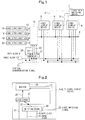
- Figs. 1 to 6 are drawings illustrating a first embodiment of a video transmission apparatus according to the present invention.
- n the n represents an integer of 2 or more
- the video display device 5 comprising; a latch signal generation circuit 40 for generating a latch signal 27 for latching either one of the n number of different video data 13, 15, 17, 19 on the transmission line 8 in accordance with a video switching signal output 2 (28) from the video data switching device 1, and a latch circuit 37 for latching a prescribed video data on the transmission line 8 by the latch signal 27.
- a video transmission apparatus in which an n (the n represents an integer of 2 or more) number of different video data 13, 15, 17, 19 are transmitted via a single transmission line 8 from a plurality of video signal output sections 14, 16, 18, 20 to a video display device 5 and on the video display device 5, the video data that is indicated by a video data switching device 1 is selectively displayed, wherein the video signal output section comprising; a delay means 24 for delaying a phase pulse 10 for controlling a transmission timing of the video signal output section (n-1) times, and generating an (n-1) number of delay pulses 23, 22, 21, each delay time of which is different from one another, respectively, and a selector 12 for sequentially selecting a prescribed video data so as to perform time division of the n number of different video data 13, 15, 17, 19, in accordance with the phase pulse 10 and the (n-1) number of delay pulses 23, 22, 21, and the video display device 5 comprising; a latch signal generation circuit 40 for generating a latch signal 27 for latching either one of the n number of different video
- a video transmission apparatus in which an n (the n represents an integer of 2 or more) number of different video data 13, 15, 17, 19 are transmitted via a single transmission line 8 from a plurality of video signal output sections 14, 16, 18, 20 to a video display device 5 and on the video display device 5, the video data that is indicated by a video data switching device 1 is selectively displayed, wherein the video display device 5 comprising; a latch signal generation circuit 40 for delaying a phase pulse 10 for controlling a receiving timing of the video display device 5 (n-1) times, and generating an (n-1) number of delay pulses 32, 31, 30, each delay time of which is different from one another, respectively, a selector 29 for selecting either one of the (n-1) number of delay pulses 32, 31, 30 and the phase pulse 10 in accordance with the video switching signal 2 output from the video data switching device 1, and a latch circuit 37 for latching a prescribed video data 13, 15, 17, 19 on the transmission line 8 by an output signal 27 from the selector 29.
- the video display device 5 comprising; a latch signal
- Fig. 1 is a block diagram of the present invention.
- Selection signals 21 to 23 from a timing clock generator 24 and the phase clock 10 operationally switch the 4-input/1-output selector 12, and video signals from a plurality of video output devices 14, 16, 18 and 20 are transmitted onto a video data transmission line 8 from the 4-input/1-output selector 12 by being sequentially time-divided.
- the video data switching device 1 instructs video display devices 5, 6 and 7 to display video data to be displayed on the video data transmission line 8, by outputting video switching signals 2, 3 and 4, respectively.
- Fig. 2 is a block diagram illustrating the video display device 5, 6, or 7 of Fig. 1.
- the latch circuit 37 latches the video data on the transmission line 8 at the rising edge of an output 27 from switching means 40, and outputs the thus-latched video data 25 to a monitor 39.
- the vertical synchronization signal 11 and the output 27 are input to the monitor 39, thereby generating a horizontal synchronization signal that suits to the size of the monitor 39.
- the monitor 39 makes a display of the contents of the video data 25 according to the thus-generated horizontal synchronization signal and the vertical synchronization signal 11.
- Fig. 3 is a block diagram illustrating the construction of the timing clock generator 24 of Fig. 1.
- Reference numerals 38, 37, and 36 each denote a flip-flop.
- the flip-flop 38 latches the phase clock 10 at the rising edge of a data clock 9. And it outputs to the selector 12 a phase clock 23 that has been delayed one clock with respect to the phase clock 10.
- the flip-flop 37 outputs to the selector 12 a phase clock 22 that has been delayed two clocks with respect to the phase clock 10.
- the flip-flop 36 outputs to the selector 12 a phase clock 21 that has been delayed three clocks with respect to the phase clock 10.
- Fig. 4 illustrates the latch circuit 37 of Fig. 2.
- a flip-flop 26 latches video data of the video data transmission line 8 at the rising edge of the output 27 from the switching means 40 and outputs the thus-latched video data 25.
- Fig. 5 illustrates the switching means 40 of Fig. 2.
- Reference numerals 35, 34, and 33 each denote a flip-flop.
- the flip-flop 35 latches the phase clock 10 at the rising edge of a data clock 9 and outputs to the selector 29 a phase clock 32 that has been delayed one clock with respect to the phase clock 10.
- the flip-flop 34 outputs to the selector 29 a phase clock 31 that has been delayed two clocks with respect to the phase clock 10.
- the flip-flop 33 outputs to the selector 29 a phase clock 30 that has been delayed three clocks with respect to the phase clock 10.
- phase clock 10 and the phase clocks 32, 31, and 30 are input to the selector 29, and in accordance with the video switching signal 28 from the video data switching device 1, either one of those clocks is selected by the selector 29 and the selected clock is output as the output 27.
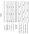
- Fig. 6 is a timing chart in which a video data 1 is displayed on the video display device 5, a video data 2 is displayed on the video display device 6, and a video data 3 is displayed on the video display device 7.
- the video output circuits 14, 16, 18 and 20 each output a picture, the size of which is the same and the frame frequency of which is the same.
- An initial pixel of a 1-frame of the video data is synchronized with the vertical synchronization signal 11.
- Each pixel of the video data is synchronized with the data clock 9.
- the vertical synchronization signal 11 and the phase clock 10 are each synchronized with the data clock 9.
- the video data 13, 15, 17 and 19 output from the video output circuits 14, 16, 18 and 20 are each renewed at the frequency of one time every four periods of the data clock.
- the video data 13, 15, 17 and 19 are sequentially time-divided every one period of the data clock 9 in accordance with the phase clocks 10, 23, 22 and 21, thereby the video data 13, 15, 17, and 19 are sequentially output onto the video data transmission line 8 from the 4-input/1-output selector 12. Accordingly, in synchronization with the data clock 9, the video data A, D, G, J, B, E, H and K are output onto the video data transmission line 8 in the order mentioned.
- the video data switching device 1 outputs the video switching signal 2 (the symbol 28 of Fig. 5) so that the 4-input/1-output selector 29 of Fig. 5 selects the phase clock 10. Accordingly, the phase clock 10 is output as the output signal 27 of Fig. 5 (or Fig. 2) from the 4-input/1-output selector 29.
- the latch circuit 37 of Fig. 2 latches the data A of the video data 13 of the video data transmission line 8 at the rising edge of the output 27, i.e. the rising edge of the phase clock 10.
- the latched data A is output to the monitor 39 of the video display device 5 and is displayed thereon.
- the data B of the video data 13 of the video data transmission line 8 is latched at the rising edge of the phase clock 10.
- the latched data is output to the monitor. In this way, the video data 13 is sequentially latched at the rising edge of the phase clock 10, and the latched data is displayed on the monitor 39 of the video display device 5.
- the video data switching device 1 outputs the video switching signal 3 (the symbol 28 of Fig. 5) so that the 4-input/1-output selector 29 of Fig. 5 selects the phase clock 32 that has been delayed by one period of the data clock.
- the latch circuit 37 latches the data D of the video data 15 of the video data transmission line 8 at the rising edge of the phase clock 32.
- the latched data D is output to the monitor 39 of the video display device 6 and is displayed thereon.
- the data E of the video data 15 of the video data transmission line 8 is latched at the rising edge of the phase clock 32.
- the latched data E is output to the monitor. In this way, the video data 15 is sequentially latched at the rising edge of the phase clock 32, and the latched data is displayed on the monitor 39 of the video display device 6.
- the video data 15 is sequentially input to the monitor 39 from the latch circuit 37, thereby the video data 15 is displayed on the video display device 6.
- the video data switching device 1 outputs a video switching signal 4 so that the 4-input/1-output selector 29 of Fig. 5 selects the phase clock 31 that has been delayed by two periods of the data clock.
- the thereafter-succeeding operations are the same as in the case of each of the video display devices 5 and 6.
- the video data 13 output from the video output device 14 is output onto the video transmission line 8 as described above, the data transmission rate thereof becomes 4 times higher.
- the data transmission rate when inputting the video data 13 to the monitor 39 is decreased to 1/4, so that it is possible to use a conventional-standard device such as an NTSC, and therefore it becomes possible to perform multiplex transmission at a low cost.
- Figs. 7 to 14 are drawings illustrating a second embodiment of the video transmission apparatus according to the present invention.
- an m (the m represents an integer of 2 or more) number of different video data 65-75 having a small picture-image size and a first number of pixels, and a video data 63 having a large picture-image size and a second number of pixels, pixels number of which is m times as great as said first number of pixels, are transmitted via a single transmission line 58 to a plurality of video display devices 55-57, on a first video display device 56 for displaying the video data 65-75 having the first number of pixels, the video data that is indicated by a video data switching device 51 is selectively displayed, and on a second video display device 55 for displaying the video data 63 having the second number of pixels, the video data 63 having the second number of pixels is displayed, wherein the first video display device 56 (referred to as an "SD video display device") comprising; a latch signal generation circuit 158 for generating a first latch signal 110 for latching either one of the m number of different video data (referred to as an SD video display device) comprising; a latch signal generation
- a video transmission apparatus having a first video display device 56 and a second video display device 55
- the first video display device 56 comprising; a latch signal generation circuit 158 for delaying a phase pulse 60 for controlling a receiving timing of the video display device 56 m times, and generating an m number of delay pulses 118-113, each delay time of which is different from one another, respectively, a selector 111 for selecting either one of the m number of delay pulses 118-113 in accordance with the video switching signal 53 (112) output from the video data switching device 51, and a latch circuit 157 for latching the video data 65-75 having the first number of pixels on the transmission line 58 by an output signal 110 from the selector 111, and the second video display device 55 comprising; a latch signal generation circuit 154 for delaying a phase pulse 60 for controlling a receiving timing of the video display device 55 (m-1) times, and generating an (m-1) number of delay pulses 92-88, each delay time of which is different from one another
- Fig. 7 illustrates an example in which the following two kinds of picture-image data, the sizes of which differ from each other, are multiplex-transmitted and displayed.
- One kind of picture image data has a small picture-image size of horizontal 720 pixels and vertical 480 lines and a first number of pixels.
- the other kind of picture image data has a large picture-image size of horizontal 1920 pixels and vertical 1080 lines and a second number of pixels.
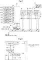
- Fig. 8 shows the block diagram of a video display device for use for the video data, the size of which is large and that has the second number of pixels.
- the latch circuit 152 latches video data on the transmission line 58 at the rising edge of the output signal 86 from the HD switching means (the latch signal generation circuit) 154.
- the latched signal 151 is output to the HD monitor 150.
- the vertical synchronization signal 61 and the output signal 86 are input to the monitor 150, thereby producing a horizontal synchronization signal that suits to the size of the monitor.
- the monitor 150 makes a display of the contents of the video data 151 in accordance with the produced horizontal synchronization signal and the vertical synchronization signal 61.
- Fig. 9 shows the block diagram of a video display device for use for the video data, the size of which is small and that has the first number of pixels.
- the latch circuit 157 latches video data on the transmission line 58 at the rising edge of the output signal 110 from the SD switching means (the latch signal generation circuit) 158.
- the latched signal 156 is output to the SD monitor 155.
- the vertical synchronization signal 61 and the output signal 110 are input to the monitor 155, thereby producing a horizontal synchronization signal that suits to the size of the monitor.
- the monitor 150 makes a display of the contents of the video data 156 in accordance with the produced horizontal synchronization signal and the vertical synchronization signal 61.
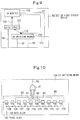
- Fig. 10 shows the HD switching means 154 of Fig. 8, which performs OR operation of the following six signals by the OR circuit 87 so as to generate the HD switching output signal 86.
- input signals of the OR circuit 87 are the phase clock 60, the phase clock 92 that has been delayed by two periods of the data clock, the phase clock 91 that has been delayed by four periods of the data clock, the phase clock 90 that has been delayed by six periods of the data clock, the phase clock 89 that has been delayed by eight periods of the data clock, and the phase clock 88 that has been delayed by ten periods of the data clock.
- Fig. 11 shows the SD switching means 158 of Fig. 9, which produces the following phase clock signals.
- the SD switching means 158 selects a prescribed one clock from those phase clock signals in accordance with the video switching signal 112. And selected clock is output as the switcher output signal 110 to the latch circuit 152.
- Those phase clock signals are the phase clock 118 that has been delayed by one period of the data clock 59, the phase clock 117 that has been delayed by three periods of the data clock 59, the phase clock 116 that has been delayed by five periods of the data clock 59, the phase clock 115 that has been delayed by seven periods of the data clock 59, the phase clock 114 that has been delayed by nine periods of the data clock 59, and the phase clock 113 that has been delayed by eleven periods of the data clock 59.
- Fig. 12 is a block diagram showing a multiplexing circuit on the signal transmission side.
- transmission means 200 for transmitting the video data 63 having the second number of pixels and a large picture image size onto the transmission line 58 at intervals
- transmission means 300 for sequentially transmitting six pieces of video data 65, 67, 69, 71, 73 and 75 having a small picture image size and the first number of pixels onto the transmission line 58, when the video data 63 having the second pixels number are not being transmitted.
- Those video data are multiplexed and transmitted.
- Fig. 13 is a timing chart in which, the HD video data 63 is displayed on the HD video display device 55 and the SD video data 65 is displayed on the SD video display device 56.
- the SD picture-image output circuits 66, 68, 70, 72, 74 and 76 each are outputting the same size of picture image.
- the HD picture-image output circuit 64 is outputting pixels that are six times as large in number as those of one SD picture-image output circuit at a speed that is six times as high.
- An initial pixel of the video data is synchronized with the vertical synchronization signal 61, and each pixel of the video data is synchronized with the data clock 59. Also, the vertical synchronization signal 61 and the phase clock 60 are each synchronized with the data clock 59.
- the video data 65, 67, 69, 71, 73 and 75 each are renewed at the frequency of one time per 12 periods of the data clock 59.
- the video data 63 is renewed at the frequency of one time per 2 periods of the data clock.
- the video data is time-divided per one period of the data clock and is multiplexed in the order of A, L, B, N, C, P, D, R, E, T, F, V, G and M. Then, the time-divided picture image data are output to the video data transmission line 58 in that order.
- the output 86 of the 6-input OR circuit 87 of Fig. 10 becomes 6 times as high in frequency as the phase clock 60 as illustrated in the timing chart of Fig. 13.
- the latch circuit 152 of Fig. 8 latches the HD picture images on the transmission line 58, so that, the picture image data, the number of pixels of which is large become able to be reproduced on the video display device 55 in the order of A, B, C, D, E and F.
- the video data switching device 51 outputs the video switching signal 53 (the symbol 112 of Fig. 11) so that the 6-input/1-output selector 111 of Fig. 11 selects the phase clock 118 that has been delayed by one period of the data block 59. Accordingly, the picture image data L is reproduced on the SD video display device 56, and, further, after 12 clocks, the picture image data M is reproduced on the SD video display device 56. Also, when the video data 67 is displayed on the SD video display device 57, the video data switching device 51 outputs the video switching signal 54 so that the 6-input/1-output selector 111 of Fig.
- the picture image data N is reproduced on the SD video display device 57, and, further, after 12 clocks, the picture image data O is reproduced on the SD video display device 57.
- the video data output from the HD video output device 64 and the video data output from the SD video output devices 66 to 76 are transmitted onto the transmission line 58 by being multiplexed. Therefore, the transmission rate of the HD video data becomes twice as high, and the transmission rate of the SD video data becomes 12 times as high.
- the transmission rate of input data to the HD monitor 150 is made 1/2 as high, so that, with respect to the video output device 64 and the HD monitor 150, there can be used the ones having the same standard as in the prior art, respectively. Therefore, it is possible to achieve the cost reduction.
- the data rate is made 1/12 as high.
- Fig. 14 is a timing chart in which five pieces of SD video data (2)-(5), the pixels number of which is the smallest, another SD video data (1), the pixels number of which is twice as great as that of the SD video data (2)-(5), and the above-described HD video data are multiplexed and respective ones of these video data are displayed.
Landscapes
- Engineering & Computer Science (AREA)
- Theoretical Computer Science (AREA)
- Human Computer Interaction (AREA)
- Physics & Mathematics (AREA)
- General Engineering & Computer Science (AREA)
- General Physics & Mathematics (AREA)
- Control Of Indicators Other Than Cathode Ray Tubes (AREA)
- Television Systems (AREA)
- Studio Circuits (AREA)
Applications Claiming Priority (2)
| Application Number | Priority Date | Filing Date | Title |
|---|---|---|---|
| JP2000179786 | 2000-06-15 | ||
| JP2000179786A JP2001359056A (ja) | 2000-06-15 | 2000-06-15 | 映像伝送装置 |
Publications (2)
| Publication Number | Publication Date |
|---|---|
| EP1164787A2 true EP1164787A2 (de) | 2001-12-19 |
| EP1164787A3 EP1164787A3 (de) | 2004-06-23 |
Family
ID=18680993
Family Applications (1)
| Application Number | Title | Priority Date | Filing Date |
|---|---|---|---|
| EP01114492A Withdrawn EP1164787A3 (de) | 2000-06-15 | 2001-06-15 | Video-Übertragungsgerät |
Country Status (3)
| Country | Link |
|---|---|
| US (1) | US20020001041A1 (de) |
| EP (1) | EP1164787A3 (de) |
| JP (1) | JP2001359056A (de) |
Cited By (1)
| Publication number | Priority date | Publication date | Assignee | Title |
|---|---|---|---|---|
| CN103327282A (zh) * | 2013-07-22 | 2013-09-25 | 苏州硅智源微电子有限公司 | 增加放大器非工作状态输出阻抗的方法 |
Families Citing this family (7)
| Publication number | Priority date | Publication date | Assignee | Title |
|---|---|---|---|---|
| US20060190528A1 (en) * | 2003-03-11 | 2006-08-24 | Pugel Michael A | Apparatus and method for distributing signals |
| JP2005073077A (ja) * | 2003-08-26 | 2005-03-17 | Sharp Corp | 固体撮像装置 |
| JP2007311929A (ja) * | 2006-05-16 | 2007-11-29 | Sony Corp | 映像送出装置、映像送出方法、映像受信装置及び映像受信方法 |
| US20080063144A1 (en) * | 2006-09-07 | 2008-03-13 | General Electric Company | Method and system for simultaneously illustrating multiple visual displays |
| JP2011217062A (ja) * | 2010-03-31 | 2011-10-27 | Sony Corp | カメラシステム、信号遅延量調整方法及びプログラム |
| US9549015B2 (en) * | 2014-04-15 | 2017-01-17 | Lattice Semiconductor Corporation | Communication of multimedia data streams over multiple communication lanes |
| CN108391031B (zh) * | 2018-01-17 | 2023-03-10 | 中国北方车辆研究所 | 一种视频滚动显示装置和方法 |
Family Cites Families (5)
| Publication number | Priority date | Publication date | Assignee | Title |
|---|---|---|---|---|
| US5325131A (en) * | 1993-05-03 | 1994-06-28 | Tektronix, Inc. | Multiformat television switcher |
| JPH1028256A (ja) * | 1996-07-11 | 1998-01-27 | Matsushita Electric Ind Co Ltd | 映像信号変換装置とテレビジョン信号処理装置 |
| JPH1098708A (ja) * | 1996-09-20 | 1998-04-14 | Fujitsu General Ltd | 映像監視装置 |
| JP3317176B2 (ja) * | 1997-02-06 | 2002-08-26 | 松下電器産業株式会社 | 映像伝送装置 |
| JPH11146273A (ja) * | 1997-11-06 | 1999-05-28 | Fujitsu General Ltd | 映像切替装置 |
-
2000
- 2000-06-15 JP JP2000179786A patent/JP2001359056A/ja active Pending
-
2001
- 2001-06-14 US US09/879,924 patent/US20020001041A1/en not_active Abandoned
- 2001-06-15 EP EP01114492A patent/EP1164787A3/de not_active Withdrawn
Cited By (1)
| Publication number | Priority date | Publication date | Assignee | Title |
|---|---|---|---|---|
| CN103327282A (zh) * | 2013-07-22 | 2013-09-25 | 苏州硅智源微电子有限公司 | 增加放大器非工作状态输出阻抗的方法 |
Also Published As
| Publication number | Publication date |
|---|---|
| US20020001041A1 (en) | 2002-01-03 |
| EP1164787A3 (de) | 2004-06-23 |
| JP2001359056A (ja) | 2001-12-26 |
Similar Documents
| Publication | Publication Date | Title |
|---|---|---|
| US5594467A (en) | Computer based display system allowing mixing and windowing of graphics and video | |
| US6141062A (en) | Method and apparatus for combining video streams | |
| US5027212A (en) | Computer based video/graphics display system | |
| US4949169A (en) | Audio-video data interface for a high speed communication link in a video-graphics display window environment | |
| EP0762325B1 (de) | Videovergrösserungsgerät | |
| US6593939B2 (en) | Image display device and driver circuit therefor | |
| JPH087567B2 (ja) | 画像表示装置 | |
| JPH06209438A (ja) | 高品位テレビを利用した多重再生方法および多重再生装置 | |
| US5627825A (en) | Video communication apparatus | |
| US4500908A (en) | Method and apparatus for standardizing nonstandard video signals | |
| KR940006419A (ko) | 컬러화상, 표시장치 | |
| CN101778199A (zh) | 一种合成多路高清视频图像画面的实现方法 | |
| EP1164787A2 (de) | Video-Übertragungsgerät | |
| JP4445122B2 (ja) | 2タップ/3タップフリッカフィルタリングのためのシステム及び方法 | |
| US5739868A (en) | Apparatus for processing mixed YUV and color palettized video signals | |
| US3745242A (en) | Multiplex tv system for transmitting and receiving a plurality of pictures on a line sharing basis | |
| US4943856A (en) | Method and apparatus for introducing a pan and scan feature to high definition television systems | |
| JP3154190B2 (ja) | 汎用走査周期変換装置 | |
| US5896178A (en) | Method and system for converting VGA signals to television signals including horizontally averaging and thinning scanning lines before vertically averaging the scanning lines | |
| JP2004538741A (ja) | 複数セットの多重チャネルデジタル画像を組み合わせる方法及びバスインタフェース技術 | |
| JPH09247574A (ja) | 走査線変換装置 | |
| JPH118799A (ja) | ビデオ表示制御装置 | |
| JPH03135182A (ja) | 映像伝送方式 | |
| JP3113464B2 (ja) | テレビジョン受信機 | |
| JP2000341651A (ja) | フォーマット変換装置 |
Legal Events
| Date | Code | Title | Description |
|---|---|---|---|
| PUAI | Public reference made under article 153(3) epc to a published international application that has entered the european phase |
Free format text: ORIGINAL CODE: 0009012 |
|
| AK | Designated contracting states |
Kind code of ref document: A2 Designated state(s): AT BE CH CY DE DK ES FI FR GB GR IE IT LI LU MC NL PT SE TR |
|
| AX | Request for extension of the european patent |
Free format text: AL;LT;LV;MK;RO;SI |
|
| RAP1 | Party data changed (applicant data changed or rights of an application transferred) |
Owner name: NEC ELECTRONICS CORPORATION |
|
| PUAL | Search report despatched |
Free format text: ORIGINAL CODE: 0009013 |
|
| AK | Designated contracting states |
Kind code of ref document: A3 Designated state(s): AT BE CH CY DE DK ES FI FR GB GR IE IT LI LU MC NL PT SE TR |
|
| AX | Request for extension of the european patent |
Extension state: AL LT LV MK RO SI |
|
| 17P | Request for examination filed |
Effective date: 20040513 |
|
| AKX | Designation fees paid |
Designated state(s): DE FR IT |
|
| 17Q | First examination report despatched |
Effective date: 20080618 |
|
| STAA | Information on the status of an ep patent application or granted ep patent |
Free format text: STATUS: THE APPLICATION HAS BEEN WITHDRAWN |
|
| 18W | Application withdrawn |
Effective date: 20080715 |