EP1168457A2 - Cellule de mémoire ferroélectrique et procédé de fabrication - Google Patents
Cellule de mémoire ferroélectrique et procédé de fabrication Download PDFInfo
- Publication number
- EP1168457A2 EP1168457A2 EP01305409A EP01305409A EP1168457A2 EP 1168457 A2 EP1168457 A2 EP 1168457A2 EP 01305409 A EP01305409 A EP 01305409A EP 01305409 A EP01305409 A EP 01305409A EP 1168457 A2 EP1168457 A2 EP 1168457A2
- Authority
- EP
- European Patent Office
- Prior art keywords
- ferroelectric
- layer
- capacitor
- forming
- electrode
- Prior art date
- Legal status (The legal status is an assumption and is not a legal conclusion. Google has not performed a legal analysis and makes no representation as to the accuracy of the status listed.)
- Withdrawn
Links
Images

Classifications
-
- H—ELECTRICITY
- H10—SEMICONDUCTOR DEVICES; ELECTRIC SOLID-STATE DEVICES NOT OTHERWISE PROVIDED FOR
- H10D—INORGANIC ELECTRIC SEMICONDUCTOR DEVICES
- H10D1/00—Resistors, capacitors or inductors
- H10D1/60—Capacitors
- H10D1/68—Capacitors having no potential barriers
- H10D1/682—Capacitors having no potential barriers having dielectrics comprising perovskite structures
-
- H—ELECTRICITY
- H10—SEMICONDUCTOR DEVICES; ELECTRIC SOLID-STATE DEVICES NOT OTHERWISE PROVIDED FOR
- H10B—ELECTRONIC MEMORY DEVICES
- H10B53/00—Ferroelectric RAM [FeRAM] devices comprising ferroelectric memory capacitors
- H10B53/30—Ferroelectric RAM [FeRAM] devices comprising ferroelectric memory capacitors characterised by the memory core region
-
- H—ELECTRICITY
- H10—SEMICONDUCTOR DEVICES; ELECTRIC SOLID-STATE DEVICES NOT OTHERWISE PROVIDED FOR
- H10D—INORGANIC ELECTRIC SEMICONDUCTOR DEVICES
- H10D1/00—Resistors, capacitors or inductors
- H10D1/60—Capacitors
- H10D1/68—Capacitors having no potential barriers
- H10D1/692—Electrodes
-
- H—ELECTRICITY
- H10—SEMICONDUCTOR DEVICES; ELECTRIC SOLID-STATE DEVICES NOT OTHERWISE PROVIDED FOR
- H10W—GENERIC PACKAGES, INTERCONNECTIONS, CONNECTORS OR OTHER CONSTRUCTIONAL DETAILS OF DEVICES COVERED BY CLASS H10
- H10W20/00—Interconnections in chips, wafers or substrates
- H10W20/01—Manufacture or treatment
- H10W20/031—Manufacture or treatment of conductive parts of the interconnections
- H10W20/0698—Local interconnections
Definitions
- the present invention relates to a ferroelectric random access memory and more particularly, to a capacitively coupled ferroelectric random access memory cell and a method for manufacturing the same.
- FRAM ferroelectric random access memory
- SRAM static random access memory
- EAROM electrically alterable read-only memory
- a ferroelectric memory cell consists of a ferroelectric capacitor and a transistor.
- the properties of a dielectric material in the FRAM provide special advantages.
- the dielectric material has a high dielectric constant and can be polarized by an electric field. The polarization remains until it is reversed by an opposite electrical field. This makes the memory non-volatile.
- a goal in designing a non-volatile ferroelectric random access memory is to realize a small die and high speed read/write at low supply voltage.
- the present invention is directed to an improved ferroelectric random access memory.
- An object of the present invention is to provide a ferroelectric random access memory cell including a ferroelectric capacitor having fast switching speeds.
- Another object of the present invention is to provide a ferroelectric capacitor with a high charge storage capability.
- Another object of the present invention is to provide a ferroelectric capacitor that has low leakage current and relatively linear capacitance dependence on voltage.
- Another object of the present invention is to provide a simplifier manufacturing process of a ferroelectric random access memory cell.
- Another object of the present invention is to provide a ferroelectric memory cell including a ferroelectric capacitor that is driven by capacitive coupling.
- a ferroelectric memory cell includes a ferroelectric capacitor including a bottom electrode, a ferroelectric layer formed on the bottom electrode and a top electrode formed on the ferroelectric layer, a high permittivity dielectric layer formed over the ferroelectric capacitor, wherein the high permittivity dielectric layer includes an encapsulation layer and completely covers the top electrode, and a local interconnect electrode formed on the encapsulation layer.
- an integrated circuit in another aspect of the present invention, includes a ferroelectric capacitor including a bottom electrode, a ferroelectric layer formed on the bottom electrode and a top electrode formed on the ferroelectric layer, a high permittivity dielectric layer formed over the ferroelectric capacitor, wherein the high permittivity dielectric layer includes an encapsulation layer and completely covers the top electrode, and a local interconnect electrode formed on the encapsulation layer.
- a method for forming an integrated circuit includes forming a ferroelectric capacitor, wherein the ferroelectric capacitor includes a bottom electrode, a ferroelectric layer formed on the bottom electrode and a top electrode formed on the ferroelectric layer, forming a high permittivity dielectric layer over the ferroelectric capacitor, wherein the high permittivity dielectric layer includes an encapsulation layer and completely covers the top electrode, and forming a local interconnect electrode on the encapsulation layer so that the top electrode, the encapsulation layer and the local interconnect electrode form a second capacitor.
- a ferroelectric memory cell in another aspect of the present invention, includes a conductive barrier, a ferroelectric capacitor formed on the conductive barrier, wherein the ferroelectric capacitor includes a bottom electrode, a ferroelectric layer formed on the bottom electrode and a top electrode formed on the ferroelectric layer, and a high permittivity dielectric layer formed between the conductive barrier and the ferroelectric capacitor, wherein the conductive barrier connects the ferroelectric capacitor to an underlying device through a connecting electrode formed directly below the ferroelectric capacitor.
- an integrated circuit in another aspect of the present invention, includes a conductive barrier, a ferroelectric capacitor formed on the conductive barrier, wherein the ferroelectric capacitor includes a bottom electrode, a ferroelectric layer formed on the bottom electrode and a top electrode formed on the ferroelectric layer, and a high permittivity dielectric layer formed between the conductive barrier and the ferroelectric capacitor, wherein the conductive barrier connects the ferroelectric capacitor to an underlying device through a connecting electrode formed directly below the ferroelectric capacitor.
- a method for forming an integrated circuit includes forming a conductor, forming a conductive barrier on the conductor, forming a high permittivity dielectric layer on the conductive barrier, and forming a ferroelectric capacitor on the high permittivity dielectric layer, wherein the ferroelectric capacitor includes a bottom electrode, a ferroelectric layer formed on the bottom electrode and a top electrode formed on the ferroelectric layer, wherein the conductive barrier connects the ferroelectric capacitor to an underlying device through the conductor.
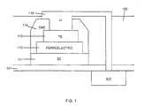
- FIG. 1 shows a cross sectional view of a ferroelectric memory cell structure including a ferrcelectric capacitor.
- the ferroelectric capacitor includes a bottom electrode 111, a ferroelectric thin film layer 112, and a top electrode 113.
- the ferroelectric capacitor is formed on an underlying layer 141, and an encapsulation layer 114 is formed over the ferroelectric capacitor to protect the ferroelectric capacitor from being damaged during etching of the bottom electrode 111.
- An interlevel dielectric layer 150 is deposited thereafter, and then the interlevel dielectric layer 150 and the encapsulation layer 114 are etched to form an opening so that a local interconnect electrode 115 can be formed to be in contact with the top electrode 113 through the opening.
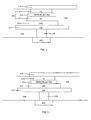
- FIG. 2 shows a cross sectional view of a ferroelectric memory cell according to a first embodiment of the present invention.
- the ferroelectric memory cell shown in FIG. 2 includes a ferroelectric capacitor 250 formed on an underlayer of an integrated circuit.
- the ferroelectric capacitor includes a bottom electrode 211 and a top electrode 213 with a ferroelectric thin film layer 212 formed between.
- the ferroelectric thin film layer 212 is formed of a ferroelectric material having a ceramic ferroelectric with a perovskite structure, such as PZT (lead zirconate titanate) or PLZT (lead lanthanum zirconate titanate).
- PZT is used to form the ferroelectric thin film layer 212 (hereinafter PZT-F layer).
- the ferroelectric memory cell is formed by forming the bottom electrode 211 on a CMOS underlayer coated with SiO 2 or other interlayer dielectric layer 210 of an integrated circuit. Thereafter, the PZT-F layer 212 is formed on the bottom electrode 211 and the top electrode 213 is formed on the PZT-F layer 212, consecutively. Thereafter, an encapsulation layer 214 formed of a high permittivity dielectric (HPD) is formed to cover and protect the underlying ferroelectric capacitor 250 from being damaged during etching of the bottom electrode 211. Then, a local interconnect electrode 215 is formed on the encapsulation layer 214 to connect the ferroelectric capacitor to a source/drain of a transistor.
- HPD high permittivity dielectric
- the ferroelectric memory cell in this embodiment includes two capacitors in series - the ferroelectric capacitor 250 and a second capacitor including the top electrode 213, the encapsulation layer 214, and the local interconnect electrode 215.
- the ferroelectric capacitor 250 switches under the applied voltage, while the second capacitor does not.
- the second capacitor is formed to have a capacitance that is 5 to 10 times larger than a capacitance of the ferroelectric capacitor 250 by varying a thickness, an area, or a dielectric permittivity of the encapsulation layer 214.
- the encapsulation layer 214 should have a dielectric permittivity that is 5 to 10 times larger than that of the PZT-F layer 212. With such a capacitance ratio between the ferroelectric capacitor and the second capacitor, most of the voltage drop is across the ferroelectric capacitor 250.
- the encapsulation layer 214 formed of high permittivity dielectric is used to form the second capacitor having a high charge storage capability that has low leakage current and relatively linear capacitance dependence on voltage.
- the high permittivity dielectric may be formed of PZT with a lower Pb concentration than that of the PZT-F layer 212, which can provide a film with reduced leakage current without a dramatic decrease in permittivity.
- the high permittivity dielectric may be formed by plasma damaging a PZT layer during etching processes of the top electrode, the bottom electrode, the PZT-F layer, and the encapsulating layer. The plasma damage can improve the linear dielectric performance of the encapsulating layer.
- the high permittivity dielectric may be formed of different compositions, which may include changes in Pb (lead), Zr (zirconium), and Ti (titanium) concentrations, as well as dopant concentrations, such as Ca (Calcium), Sr (Strontium), and La (lanthanum).
- a very thin layer of electrode may be used for the top electrode 213.
- the top electrode of the ferroelectric capacitor 250 may be completely eliminated as shown in FIG. 3. Without the top electrode, a top interface of the PZT-F layer is no longer controlled by a ferroelectric/conductor interface. A dielectric/dielectric interface can provide better process stability with respect to the ferroelectric properties.
- FIG. 4 shows a cross sectional view of a ferroelectric random access memory cell according to a second embodiment of the present invention.
- a ferroelectric capacitor is formed on a high permittivity dielectric layer. Additionally, the ferroelectric capacitor is formed directly over a connecting electrode that connects the ferroelectric capacitor to an underlying CMOS.
- the ferroelectric memory cell shown in FIG. 4 is formed by forming a connecting electrode 416 on a source/drain region of a transistor, and forming a conductive barrier 417 thereon. Thereafter, a high permittivity dielectric layer 414 is formed on the conductive barrier 417, and a ferroelectric capacitor 450 is formed on the high permittivity dielectric layer 414.
- the ferroelectric capacitor 450 includes a bottom electrode 411, a ferroelectric thin film layer 412 (PZT-F layer, for example), and a top electrode 413. Then, a metalization layer 415 is formed on the ferroelectric capacitor 450.
- the-ferroelectric memory cell in this embodiment includes two capacitors in series - the ferroelectric capacitor 450 and a second capacitor including the conductive barrier 417, the high permittivity dielectric layer 414, and the bottom electrode 411.
- the ferroelectric capacitor 450 switches under the applied voltage, while the second capacitor does not switch under the applied voltage.
- the second capacitor is formed to have a capacitance that is 5 to 10 times larger than a capacitance of the ferroelectric capacitor by varying a thickness, an area, or a dielectric permittivity of the high permittivity dielectric layer 414.
- a dielectric permittivity of the high permittivity dielectric layer should be 5 to 10 times that of the PZT-F layer. With this capacitance ratio, the most of the voltage drop is across the ferroelectric capacitor.
- the high permittivity dielectric layer between the conducting barrier and the ferroelectric capacitor, an extra barrier material is included in the structure and the processing constraints on the barrier/BE interface can be reduced. Furthermore, by forming the ferroelectric capacitor directly over the connecting electrode 416 that connects the ferroelectric capacitor to the underlying CMOS, a size of the ferroelectric memory cell is reduced.
- a very thin layer of electrode may be used for the bottom electrode 411.
- the bottom electrode may be completely eliminated as shown in FIG. 5. Without the bottom electrode, the bottom interface of the PZT-F layer 412 is no longer controlled by a ferroelectric/conductor interface. A dielectric/dielectric interface can provide better process stability with respect to the ferroelectric properties.
- a capacitive coupling is used to provide the required switching voltage for a ferroelectric capacitor.
- the ferroelectric capacitor is driven by the capacitive coupling. Since a total capacitance of the ferroelectric memory cell is reduced, a RC time constant for a circuit is reduced and the ferroelectric capacitor can be switched at higher speeds. Further, by using the encapsulation layer formed of a high permittivity dielectric, a capacitor with a high storage capability can be formed. Furthermore, by a process wherein the encapsulation layer for the ferroelectric capacitor is not etched, the encapsulation layer can provide better protection of the underlying ferroelectric capacitor and a manufacturing process is simplified.
- ferroelectric capacitor directly over the connecting electrode, a size of the ferroelectric memory cell can be reduced, and by placing the high permittivity dielectric layer between the conducting barrier and the ferroelectric capacitor, the processing constraints on the conducting barrier/bottom electrode interface can be relaxed.
Landscapes
- Semiconductor Memories (AREA)
- Semiconductor Integrated Circuits (AREA)
Applications Claiming Priority (4)
| Application Number | Priority Date | Filing Date | Title |
|---|---|---|---|
| US21420700P | 2000-06-26 | 2000-06-26 | |
| US214207P | 2000-06-26 | ||
| US873772 | 2001-06-04 | ||
| US09/873,772 US6597028B2 (en) | 2000-06-26 | 2001-06-04 | Capacitively coupled ferroelectric random access memory cell and a method for manufacturing the same |
Publications (2)
| Publication Number | Publication Date |
|---|---|
| EP1168457A2 true EP1168457A2 (fr) | 2002-01-02 |
| EP1168457A3 EP1168457A3 (fr) | 2004-05-19 |
Family
ID=26908778
Family Applications (1)
| Application Number | Title | Priority Date | Filing Date |
|---|---|---|---|
| EP01305409A Withdrawn EP1168457A3 (fr) | 2000-06-26 | 2001-06-21 | Cellule de mémoire ferroélectrique et procédé de fabrication |
Country Status (3)
| Country | Link |
|---|---|
| US (1) | US6597028B2 (fr) |
| EP (1) | EP1168457A3 (fr) |
| JP (1) | JP2002141479A (fr) |
Families Citing this family (5)
| Publication number | Priority date | Publication date | Assignee | Title |
|---|---|---|---|---|
| JP4025829B2 (ja) * | 2000-09-18 | 2007-12-26 | 富士通株式会社 | 半導体装置及びその製造方法 |
| US8552515B2 (en) | 2011-08-12 | 2013-10-08 | Cypress Semiconductor Corporation | Method for fabricating a damascene self-aligned ferroelectric random access memory (F-RAM) device structure employing reduced processing steps |
| US8518792B2 (en) | 2011-08-12 | 2013-08-27 | Cypress Semiconductor Corporation | Method for fabricating a damascene self-aligned ferroelectric random access memory (F-RAM) having a ferroelectric capacitor aligned with a three dimensional transistor structure |
| US8518791B2 (en) | 2011-08-12 | 2013-08-27 | Cypress Semiconductor Corporation | Method for fabricating a damascene self-aligned ferroelectric random access memory (F-RAM) with simultaneous formation of sidewall ferroelectric capacitors |
| US8916434B2 (en) | 2012-05-11 | 2014-12-23 | Cypress Semiconductor Corporation | Enhanced hydrogen barrier encapsulation method for the control of hydrogen induced degradation of ferroelectric capacitors in an F-RAM process |
Family Cites Families (32)
| Publication number | Priority date | Publication date | Assignee | Title |
|---|---|---|---|---|
| JPH0582801A (ja) * | 1991-09-20 | 1993-04-02 | Rohm Co Ltd | 半導体集積回路のキヤパシタおよびこれを用いた不揮発性メモリ |
| US5206788A (en) * | 1991-12-12 | 1993-04-27 | Ramtron Corporation | Series ferroelectric capacitor structure for monolithic integrated circuits and method |
| BE1007902A3 (nl) * | 1993-12-23 | 1995-11-14 | Philips Electronics Nv | Schakelelement met geheugen voorzien van schottky tunnelbarriere. |
| US5977577A (en) | 1994-11-15 | 1999-11-02 | Radiant Technologies, Inc | Ferroelectric based memory devices utilizing low curie point ferroelectrics and encapsulation |
| US6194751B1 (en) | 1994-11-15 | 2001-02-27 | Radiant Technologies, Inc | Ferroelectric based memory devices utilizing low Curie point ferroelectrics and encapsulation |
| EP0972309A4 (fr) * | 1995-06-28 | 2000-01-19 | Telcordia Tech Inc | Couche barriere pour condensateur ferroelectrique integre sur silicium |
| JPH09102591A (ja) * | 1995-07-28 | 1997-04-15 | Toshiba Corp | 半導体装置及びその製造方法 |
| US5757042A (en) | 1996-06-14 | 1998-05-26 | Radiant Technologies, Inc. | High density ferroelectric memory with increased channel modulation and double word ferroelectric memory cell for constructing the same |
| US6027947A (en) * | 1996-08-20 | 2000-02-22 | Ramtron International Corporation | Partially or completely encapsulated top electrode of a ferroelectric capacitor |
| US5864932A (en) | 1996-08-20 | 1999-02-02 | Ramtron International Corporation | Partially or completely encapsulated top electrode of a ferroelectric capacitor |
| US5920453A (en) | 1996-08-20 | 1999-07-06 | Ramtron International Corporation | Completely encapsulated top electrode of a ferroelectric capacitor |
| EP0837504A3 (fr) | 1996-08-20 | 1999-01-07 | Ramtron International Corporation | Dispositif ferroélectrique partiellement ou complètement encapsulé |
| US5990513A (en) | 1996-10-08 | 1999-11-23 | Ramtron International Corporation | Yield enhancement technique for integrated circuit processing to reduce effects of undesired dielectric moisture retention and subsequent hydrogen out-diffusion |
| KR100413805B1 (ko) * | 1996-10-31 | 2004-06-26 | 삼성전자주식회사 | 누설전류를이용한매트릭스형다진법강유전체랜덤액세서메모리 |
| KR100218275B1 (ko) | 1997-05-09 | 1999-09-01 | 윤종용 | 벌크형 1트랜지스터 구조의 강유전체 메모리소자 |
| KR100243294B1 (ko) | 1997-06-09 | 2000-02-01 | 윤종용 | 반도체장치의 강유전체 메모리 셀 및 어레이 |
| JP3484324B2 (ja) * | 1997-07-29 | 2004-01-06 | シャープ株式会社 | 半導体メモリ素子 |
| JP3319994B2 (ja) * | 1997-09-29 | 2002-09-03 | シャープ株式会社 | 半導体記憶素子 |
| US6462931B1 (en) * | 1997-10-23 | 2002-10-08 | Texas Instruments Incorporated | High-dielectric constant capacitor and memory |
| JP3098474B2 (ja) * | 1997-10-31 | 2000-10-16 | 日本電気株式会社 | 半導体装置の製造方法 |
| US6313539B1 (en) * | 1997-12-24 | 2001-11-06 | Sharp Kabushiki Kaisha | Semiconductor memory device and production method of the same |
| DE19805712A1 (de) | 1998-02-12 | 1999-08-26 | Siemens Ag | Speicherzellenanordnung und entsprechendes Herstellungsverfahren |
| US6249014B1 (en) | 1998-10-01 | 2001-06-19 | Ramtron International Corporation | Hydrogen barrier encapsulation techniques for the control of hydrogen induced degradation of ferroelectric capacitors in conjunction with multilevel metal processing for non-volatile integrated circuit memory devices |
| US6174735B1 (en) | 1998-10-23 | 2001-01-16 | Ramtron International Corporation | Method of manufacturing ferroelectric memory device useful for preventing hydrogen line degradation |
| US6225656B1 (en) * | 1998-12-01 | 2001-05-01 | Symetrix Corporation | Ferroelectric integrated circuit with protective layer incorporating oxygen and method for fabricating same |
| US6281535B1 (en) * | 1999-01-22 | 2001-08-28 | Agilent Technologies, Inc. | Three-dimensional ferroelectric capacitor structure for nonvolatile random access memory cell |
| US6348709B1 (en) * | 1999-03-15 | 2002-02-19 | Micron Technology, Inc. | Electrical contact for high dielectric constant capacitors and method for fabricating the same |
| US6066868A (en) | 1999-03-31 | 2000-05-23 | Radiant Technologies, Inc. | Ferroelectric based memory devices utilizing hydrogen barriers and getters |
| US6121648A (en) | 1999-03-31 | 2000-09-19 | Radiant Technologies, Inc | Ferroelectric based memory devices utilizing hydrogen getters and recovery annealing |
| US6242299B1 (en) | 1999-04-01 | 2001-06-05 | Ramtron International Corporation | Barrier layer to protect a ferroelectric capacitor after contact has been made to the capacitor electrode |
| JP3211809B2 (ja) * | 1999-04-23 | 2001-09-25 | ソニー株式会社 | 半導体記憶装置およびその製造方法 |
| KR100333667B1 (ko) * | 1999-06-28 | 2002-04-24 | 박종섭 | 강유전체 메모리 소자의 캐패시터 제조 방법 |
-
2001
- 2001-06-04 US US09/873,772 patent/US6597028B2/en not_active Expired - Lifetime
- 2001-06-21 EP EP01305409A patent/EP1168457A3/fr not_active Withdrawn
- 2001-06-25 JP JP2001191635A patent/JP2002141479A/ja active Pending
Also Published As
| Publication number | Publication date |
|---|---|
| EP1168457A3 (fr) | 2004-05-19 |
| US20020000586A1 (en) | 2002-01-03 |
| US6597028B2 (en) | 2003-07-22 |
| JP2002141479A (ja) | 2002-05-17 |
Similar Documents
| Publication | Publication Date | Title |
|---|---|---|
| TW479311B (en) | Semiconductor high dielectric constant decoupling capacitor structures and process for fabrication | |
| KR100442892B1 (ko) | 스택 셀을 위한 보호 베리어를 갖는 반도체 장치 | |
| KR100268453B1 (ko) | 반도체 장치 및 그것의 제조 방법 | |
| US5721700A (en) | Non-volatile semiconductor memory device in which applied voltage to ferroelectric capacitor is adjusted | |
| KR100360592B1 (ko) | 반도체 장치 및 그 제조 방법 | |
| CN100362626C (zh) | 插塞结构之电容器阻障 | |
| JP3627640B2 (ja) | 半導体メモリ素子 | |
| CN1329756A (zh) | 铁电存储器场效应晶体管器件及其制作方法 | |
| US6597028B2 (en) | Capacitively coupled ferroelectric random access memory cell and a method for manufacturing the same | |
| US6492673B1 (en) | Charge pump or other charge storage capacitor including PZT layer for combined use as encapsulation layer and dielectric layer of ferroelectric capacitor and a method for manufacturing the same | |
| CN1192438C (zh) | 铁电体晶体管及存储单元 | |
| JP4073912B2 (ja) | 直列に接続されたメモリーセルを備えた強誘電体メモリー | |
| US12069867B2 (en) | Ferroelectric random access memory device with seed layer | |
| KR100624884B1 (ko) | 반도체 기억장치 | |
| CN115802760A (zh) | 基于氧化物半导体的铁电存储器 | |
| KR100197564B1 (ko) | 강유전체 커패시터 반도체 메모리 장치 및 그 제조방법 | |
| JP3611446B2 (ja) | 半導体記憶装置 | |
| KR100219532B1 (ko) | 강유전체 메모리 장치 및 그 제조방법 | |
| CN121218603A (zh) | 三维存储阵列及其制备方法、电子设备 | |
| KR100421898B1 (ko) | 반도체메모리장치 | |
| CN119586344A (zh) | 半导体器件及其制备方法、存储器系统 | |
| JPH07193136A (ja) | 記憶素子 | |
| JPH09321153A (ja) | 半導体装置 | |
| KR19980045611A (ko) | 강유전체 커패시터 제조방법 | |
| KR19980068061A (ko) | 강유전체 메모리 장치 제조 방법 |
Legal Events
| Date | Code | Title | Description |
|---|---|---|---|
| PUAI | Public reference made under article 153(3) epc to a published international application that has entered the european phase |
Free format text: ORIGINAL CODE: 0009012 |
|
| AK | Designated contracting states |
Kind code of ref document: A2 Designated state(s): AT BE CH CY DE DK ES FI FR GB GR IE IT LI LU MC NL PT SE TR |
|
| AX | Request for extension of the european patent |
Free format text: AL;LT;LV;MK;RO;SI |
|
| RIN1 | Information on inventor provided before grant (corrected) |
Inventor name: EVANS, THOMAS Inventor name: FOX, GLEN |
|
| PUAL | Search report despatched |
Free format text: ORIGINAL CODE: 0009013 |
|
| AK | Designated contracting states |
Kind code of ref document: A3 Designated state(s): AT BE CH CY DE DK ES FI FR GB GR IE IT LI LU MC NL PT SE TR |
|
| AX | Request for extension of the european patent |
Extension state: AL LT LV MK RO SI |
|
| RIC1 | Information provided on ipc code assigned before grant |
Ipc: 7H 01L 27/08 B Ipc: 7H 01L 21/8246 B Ipc: 7H 01L 21/02 B Ipc: 7H 01L 27/115 B Ipc: 7H 01L 29/92 A |
|
| AKX | Designation fees paid | ||
| REG | Reference to a national code |
Ref country code: DE Ref legal event code: 8566 |
|
| STAA | Information on the status of an ep patent application or granted ep patent |
Free format text: STATUS: THE APPLICATION IS DEEMED TO BE WITHDRAWN |
|
| 18D | Application deemed to be withdrawn |
Effective date: 20050104 |