EP1170621B1 - Dispositif de guide d'onde optique intégré - Google Patents
Dispositif de guide d'onde optique intégré Download PDFInfo
- Publication number
- EP1170621B1 EP1170621B1 EP01116402A EP01116402A EP1170621B1 EP 1170621 B1 EP1170621 B1 EP 1170621B1 EP 01116402 A EP01116402 A EP 01116402A EP 01116402 A EP01116402 A EP 01116402A EP 1170621 B1 EP1170621 B1 EP 1170621B1
- Authority
- EP
- European Patent Office
- Prior art keywords
- waveguide
- region
- polymer
- refractive index
- temperature
- Prior art date
- Legal status (The legal status is an assumption and is not a legal conclusion. Google has not performed a legal analysis and makes no representation as to the accuracy of the status listed.)
- Expired - Lifetime
Links
- 230000003287 optical effect Effects 0.000 title description 2
- 229920000642 polymer Polymers 0.000 claims description 166
- 239000011521 glass Substances 0.000 claims description 49
- 238000010438 heat treatment Methods 0.000 claims description 29
- 239000000463 material Substances 0.000 claims description 23
- 239000000758 substrate Substances 0.000 claims description 19
- 230000001902 propagating effect Effects 0.000 claims description 6
- 238000001816 cooling Methods 0.000 claims description 4
- UMIVXZPTRXBADB-UHFFFAOYSA-N benzocyclobutene Chemical compound C1=CC=C2CCC2=C1 UMIVXZPTRXBADB-UHFFFAOYSA-N 0.000 claims description 2
- ZYMKZMDQUPCXRP-UHFFFAOYSA-N fluoro prop-2-enoate Chemical compound FOC(=O)C=C ZYMKZMDQUPCXRP-UHFFFAOYSA-N 0.000 claims description 2
- 239000010410 layer Substances 0.000 description 64
- VYPSYNLAJGMNEJ-UHFFFAOYSA-N Silicium dioxide Chemical compound O=[Si]=O VYPSYNLAJGMNEJ-UHFFFAOYSA-N 0.000 description 40
- 239000000377 silicon dioxide Substances 0.000 description 18
- 235000012239 silicon dioxide Nutrition 0.000 description 17
- CFAKWWQIUFSQFU-UHFFFAOYSA-N 2-hydroxy-3-methylcyclopent-2-en-1-one Chemical compound CC1=C(O)C(=O)CC1 CFAKWWQIUFSQFU-UHFFFAOYSA-N 0.000 description 13
- 238000000034 method Methods 0.000 description 10
- 238000005253 cladding Methods 0.000 description 9
- 230000005540 biological transmission Effects 0.000 description 8
- 239000001837 2-hydroxy-3-methylcyclopent-2-en-1-one Substances 0.000 description 6
- 239000004809 Teflon Substances 0.000 description 6
- 229920006362 Teflon® Polymers 0.000 description 6
- 239000006096 absorbing agent Substances 0.000 description 6
- 239000012792 core layer Substances 0.000 description 5
- 238000004519 manufacturing process Methods 0.000 description 5
- 230000008901 benefit Effects 0.000 description 4
- 238000009987 spinning Methods 0.000 description 4
- XUIMIQQOPSSXEZ-UHFFFAOYSA-N Silicon Chemical compound [Si] XUIMIQQOPSSXEZ-UHFFFAOYSA-N 0.000 description 3
- 230000008859 change Effects 0.000 description 3
- 238000009826 distribution Methods 0.000 description 3
- 230000008569 process Effects 0.000 description 3
- 229910052710 silicon Inorganic materials 0.000 description 3
- 239000010703 silicon Substances 0.000 description 3
- LVJZCPNIJXVIAT-UHFFFAOYSA-N 1-ethenyl-2,3,4,5,6-pentafluorobenzene Chemical compound FC1=C(F)C(F)=C(C=C)C(F)=C1F LVJZCPNIJXVIAT-UHFFFAOYSA-N 0.000 description 2
- QTKPMCIBUROOGY-UHFFFAOYSA-N 2,2,2-trifluoroethyl 2-methylprop-2-enoate Chemical compound CC(=C)C(=O)OCC(F)(F)F QTKPMCIBUROOGY-UHFFFAOYSA-N 0.000 description 2
- 229910004298 SiO 2 Inorganic materials 0.000 description 2
- 238000013459 approach Methods 0.000 description 2
- 239000003638 chemical reducing agent Substances 0.000 description 2
- 230000008878 coupling Effects 0.000 description 2
- 238000010168 coupling process Methods 0.000 description 2
- 238000005859 coupling reaction Methods 0.000 description 2
- 238000013461 design Methods 0.000 description 2
- 238000005530 etching Methods 0.000 description 2
- 230000005855 radiation Effects 0.000 description 2
- 238000003892 spreading Methods 0.000 description 2
- 230000007480 spreading Effects 0.000 description 2
- 239000000126 substance Substances 0.000 description 2
- 238000012546 transfer Methods 0.000 description 2
- 230000006978 adaptation Effects 0.000 description 1
- 238000003486 chemical etching Methods 0.000 description 1
- 239000011248 coating agent Substances 0.000 description 1
- 238000000576 coating method Methods 0.000 description 1
- 229910052681 coesite Inorganic materials 0.000 description 1
- 229910052906 cristobalite Inorganic materials 0.000 description 1
- 230000007547 defect Effects 0.000 description 1
- 230000001419 dependent effect Effects 0.000 description 1
- 238000011161 development Methods 0.000 description 1
- 230000018109 developmental process Effects 0.000 description 1
- 230000009977 dual effect Effects 0.000 description 1
- 230000005684 electric field Effects 0.000 description 1
- 238000005516 engineering process Methods 0.000 description 1
- 239000000835 fiber Substances 0.000 description 1
- VOZRXNHHFUQHIL-UHFFFAOYSA-N glycidyl methacrylate Chemical compound CC(=C)C(=O)OCC1CO1 VOZRXNHHFUQHIL-UHFFFAOYSA-N 0.000 description 1
- 230000010354 integration Effects 0.000 description 1
- 239000004922 lacquer Substances 0.000 description 1
- 239000000178 monomer Substances 0.000 description 1
- 239000004033 plastic Substances 0.000 description 1
- 230000009467 reduction Effects 0.000 description 1
- 239000011347 resin Substances 0.000 description 1
- 229920005989 resin Polymers 0.000 description 1
- 230000000284 resting effect Effects 0.000 description 1
- 230000000717 retained effect Effects 0.000 description 1
- 210000002023 somite Anatomy 0.000 description 1
- 229910052682 stishovite Inorganic materials 0.000 description 1
- 238000012549 training Methods 0.000 description 1
- 229910052905 tridymite Inorganic materials 0.000 description 1
- 230000003313 weakening effect Effects 0.000 description 1
Images



Classifications
-
- G—PHYSICS
- G02—OPTICS
- G02F—OPTICAL DEVICES OR ARRANGEMENTS FOR THE CONTROL OF LIGHT BY MODIFICATION OF THE OPTICAL PROPERTIES OF THE MEDIA OF THE ELEMENTS INVOLVED THEREIN; NON-LINEAR OPTICS; FREQUENCY-CHANGING OF LIGHT; OPTICAL LOGIC ELEMENTS; OPTICAL ANALOGUE/DIGITAL CONVERTERS
- G02F1/00—Devices or arrangements for the control of the intensity, colour, phase, polarisation or direction of light arriving from an independent light source, e.g. switching, gating or modulating; Non-linear optics
- G02F1/29—Devices or arrangements for the control of the intensity, colour, phase, polarisation or direction of light arriving from an independent light source, e.g. switching, gating or modulating; Non-linear optics for the control of the position or the direction of light beams, i.e. deflection
- G02F1/31—Digital deflection, i.e. optical switching
- G02F1/313—Digital deflection, i.e. optical switching in an optical waveguide structure
- G02F1/3132—Digital deflection, i.e. optical switching in an optical waveguide structure of directional coupler type
-
- G—PHYSICS
- G02—OPTICS
- G02F—OPTICAL DEVICES OR ARRANGEMENTS FOR THE CONTROL OF LIGHT BY MODIFICATION OF THE OPTICAL PROPERTIES OF THE MEDIA OF THE ELEMENTS INVOLVED THEREIN; NON-LINEAR OPTICS; FREQUENCY-CHANGING OF LIGHT; OPTICAL LOGIC ELEMENTS; OPTICAL ANALOGUE/DIGITAL CONVERTERS
- G02F1/00—Devices or arrangements for the control of the intensity, colour, phase, polarisation or direction of light arriving from an independent light source, e.g. switching, gating or modulating; Non-linear optics
- G02F1/01—Devices or arrangements for the control of the intensity, colour, phase, polarisation or direction of light arriving from an independent light source, e.g. switching, gating or modulating; Non-linear optics for the control of the intensity, phase, polarisation or colour
- G02F1/061—Devices or arrangements for the control of the intensity, colour, phase, polarisation or direction of light arriving from an independent light source, e.g. switching, gating or modulating; Non-linear optics for the control of the intensity, phase, polarisation or colour based on electro-optical organic material
- G02F1/065—Devices or arrangements for the control of the intensity, colour, phase, polarisation or direction of light arriving from an independent light source, e.g. switching, gating or modulating; Non-linear optics for the control of the intensity, phase, polarisation or colour based on electro-optical organic material in an optical waveguide structure
-
- G—PHYSICS
- G02—OPTICS
- G02F—OPTICAL DEVICES OR ARRANGEMENTS FOR THE CONTROL OF LIGHT BY MODIFICATION OF THE OPTICAL PROPERTIES OF THE MEDIA OF THE ELEMENTS INVOLVED THEREIN; NON-LINEAR OPTICS; FREQUENCY-CHANGING OF LIGHT; OPTICAL LOGIC ELEMENTS; OPTICAL ANALOGUE/DIGITAL CONVERTERS
- G02F1/00—Devices or arrangements for the control of the intensity, colour, phase, polarisation or direction of light arriving from an independent light source, e.g. switching, gating or modulating; Non-linear optics
- G02F1/01—Devices or arrangements for the control of the intensity, colour, phase, polarisation or direction of light arriving from an independent light source, e.g. switching, gating or modulating; Non-linear optics for the control of the intensity, phase, polarisation or colour
- G02F1/011—Devices or arrangements for the control of the intensity, colour, phase, polarisation or direction of light arriving from an independent light source, e.g. switching, gating or modulating; Non-linear optics for the control of the intensity, phase, polarisation or colour in optical waveguides, not otherwise provided for in this subclass
- G02F1/0113—Glass-based, e.g. silica-based, optical waveguides
-
- G—PHYSICS
- G02—OPTICS
- G02F—OPTICAL DEVICES OR ARRANGEMENTS FOR THE CONTROL OF LIGHT BY MODIFICATION OF THE OPTICAL PROPERTIES OF THE MEDIA OF THE ELEMENTS INVOLVED THEREIN; NON-LINEAR OPTICS; FREQUENCY-CHANGING OF LIGHT; OPTICAL LOGIC ELEMENTS; OPTICAL ANALOGUE/DIGITAL CONVERTERS
- G02F1/00—Devices or arrangements for the control of the intensity, colour, phase, polarisation or direction of light arriving from an independent light source, e.g. switching, gating or modulating; Non-linear optics
- G02F1/01—Devices or arrangements for the control of the intensity, colour, phase, polarisation or direction of light arriving from an independent light source, e.g. switching, gating or modulating; Non-linear optics for the control of the intensity, phase, polarisation or colour
- G02F1/0147—Devices or arrangements for the control of the intensity, colour, phase, polarisation or direction of light arriving from an independent light source, e.g. switching, gating or modulating; Non-linear optics for the control of the intensity, phase, polarisation or colour based on thermo-optic effects
Definitions
- the present invention relates to an integrated waveguide arrangement according to the preamble of claim 1, such as known from EP-A-0 980 018.
- EP-A-0 997 765 discloses an integrated waveguide arrangement with a waveguide consisting of a glass core and a jacket, a foreign area made of polymer and with a Temperature setting unit, the foreign area in the Coat is integrated.
- WO 00/28355 discloses an integrated waveguide arrangement with a glass waveguide area, in which a waveguide with a glass core and glass jacket arranged is one extending near the waveguide Foreign area made of a different material and glass with a temperature setting unit for heating and cooling the foreign area, causing the wave propagation in the waveguide can be influenced, the foreign region in the waveguide region is integrated.
- JP (A) 11237652 discloses an integrated waveguide arrangement with a waveguide consisting of glass core and Glass jacket and a foreign area made of polymer and with a Temperature setting unit, the foreign area in the Glass jacket is integrated.
- EP-A-0 992 834 discloses an integrated waveguide arrangement with a waveguide consisting of glass core and Glass jacket, a foreign area made of polymer and a temperature setting unit, where the foreign area in the glass jacket is integrated.
- the problem on which the present invention is based is explained using an integrated waveguide arrangement which contains a waveguide region, a foreign region and a temperature setting unit.
- the waveguide area consists of glass, for example SiO 2 , and contains a waveguide with a glass core and a glass jacket.
- the refractive index of the glass core is larger than the refractive index of the glass cladding.
- the waveguide is calculated so that it carries an electromagnetic wave with little loss.
- the foreign area consists of a material different from glass and extends near the waveguide. On typical distance between the foreign area and the waveguide for example 1 micron ( ⁇ m) or 2 ⁇ m.
- the temperature setting unit is used for heating and / or cooling of the foreign area, whereby the wave propagation in the Waveguide can be influenced.
- a typical work area the temperature setting unit is between -40 ° C and 150 ° C
- Such a waveguide arrangement is from the article "Hybrid switches offer the best of both worlds ", fiber systems, 05/2000, Vol.4, No.4, p.15, by Pauline Rigby.
- the wave arrangement explained there contains two waveguides Glass connected by a polymer waveguide are.
- the waveguide arrangement according to the invention when manufacturing the waveguide arrangement according to the invention only one polymer layer can be applied.
- the Manufacturing tolerances are small because digging certain Depth can be etched very accurately.
- the refractive index of the material in the foreign area is not critical, because with the large thermo-optical coefficient Set within wide limits with the help of the temperature setting unit can be.
- the integrated waveguide arrangement according to the invention opens the way for a variety of new waveguide components.
- a glass waveguide or with respect to several glass waveguides can be switch units, coupling units, Build attenuators and radiators.
- the waveguide arrangement is the waveguide area on a flat substrate arranged. On the side facing away from the substrate, the Waveguide region approximately parallel to the interface of Surface and substrate area of the waveguide.
- the waveguide arrangement can be done using the technically manufacture very sophisticated lithographic processes.
- the waveguide area contains the input process steps 1 to 4 mentioned, the intermediate layer, Parts of the core layer, namely the waveguide cores made of glass, as well as the cladding layer.
- the cladding layer forms due to flow processes when they are applied an approximately parallel surface on the side facing away from the substrate to the substrate surface.
- the foreign area will be the next training course made of a material with a thermo-optical coefficient, whose amount is substantially the same as the amount of the thermo-optical Coefficient of the glass differs.
- Coefficients used that are 100 times larger in amount than the thermo-optical coefficient of glass.
- the room temperature is 20 ° C selected.
- thermo-optical coefficient e.g. B. a fluoroacrylate polymer, the pentafluorostyrene (PFS), trifluoroethyl methacrylate (TFM) and glycidyl methacrylate (GMA) contains.
- a polymer with a negative thermo-optical coefficient is z.
- the foreign area extends from the surface of the waveguide region facing away from the substrate up to the vicinity of the waveguide. This arrangement is one Result of the applied manufacturing technology. The bringing in a trench is from the surface of the Waveguide range possible. Then the material of the foreign area in the trench, so enough it to the edge of the trench or beyond.
- the waveguide core has one larger refractive index than the waveguide cladding, and the refractive index
- the material in the external area depends on that of temperature generated by the temperature setting unit and can depend on one and the same waveguide arrangement of the operating mode, smaller, equal to or larger than that Be the refractive index of the waveguide cladding.
- the foreign area extends roughly parallel to the glass waveguide. Because waveguide and Foreign area are so close together that a the wave propagating in the waveguide is influenced the strength of both influencing the length of the route dependent, in which foreign area and waveguide roughly parallel to each other, as well as by the temperature caused refractive index in the foreign area. A variety opens up Control options and switching principles.
- the foreign area becomes upwards and to the side offset from waveguide.
- this measure must be used when using lithographic methods when etching the Trench for the outside area are not feared that the waveguide area is unintentionally destroyed, as is the The case would be if the trench was just above the waveguide would have to be etched.
- the waveguide be located within the area between the foreign area and substrate.
- thermo-optical attenuator based on a different principle works, arises when the waveguide runs along the Direction of propagation of the waves is curved.
- the foreign area is arranged on the curved areas of the waveguide.
- the temperature setting unit becomes a spreading in the glass waveguide Wave more or less pulled into the foreign area and radiates from there into the waveguide jacket.
- the waveguide is made of glass and the foreign area is about the same cross-section, so they are suitable as a waveguide for guiding the same type of wave.
- a wave can be generated with relatively low transmission losses from the glass waveguide into the foreign area or conduct in the opposite direction. This is the basis for many switching operations.
- thermo-optical switch is created with a waveguide arrangement, where the waveguide region two is roughly parallel contains waveguides between which the Foreign area is arranged.
- the foreign area can be so train small that depending on the temperature one in the wave transmitted from one waveguide into the other waveguide transfers. In the case of a small external area, the 0 transmission losses remain low in the polymer. A waveguide in the external area itself is not necessary.
- the temperature setting unit arranged directly on the foreign area.
- the temperature setting unit weakens itself in the Wave spreading foreign area and thus has in addition to the levy or absorbing heat has a dual function. Absorbing a shaft is better for many applications than the diffuse radiation of energy into the waveguide area.
- a reducer can be built, on the one hand the temperature setting unit that spreads in the foreign area Wave absorbs and in the other the material the foreign area is chosen so that it is a bad one Has transmission behavior.
- the disadvantage of the polymer larger transmission losses than a glass waveguide can therefore be used as an advantage for a reducer become.
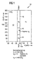
- FIG. 1 shows a top view of a thermo-optical Attenuator 10, which introduced in a waveguide layer 12 Contains waveguide cores 14 and 16.
- the waveguide layer 12 consists of silicon dioxide and has a refractive index n1 equal to 1,442. These are in the waveguide layer 12 Waveguide cores 14 and 16 embedded on all sides.
- the waveguide cores 14 and 16 also exist as silicon dioxide, however, have a refractive index n3 equal to 1.448.
- a polymer area 18 lies between the waveguide cores 14 and 16. Crosswise to the direction of propagation of a wave in the waveguide cores 14, 16 have the waveguide cores 14, 16 and the polymer region 18 has the same expansion.
- the polymer area 18 extends from the surface of the waveguide layer 12 to the surfaces of the waveguide cores 14, 16, which face a substrate, not shown.
- the Polymer region 18 has a refractive index n2 at room temperature equal to 1.5. With the help of a arranged over the polymer region 18 Heating element (not shown) can Change the value of the refractive index n2 in wide ranges, as below explained with reference to FIGS. 2A to 2C.
- the polymer region 18 consists of the material Cyclotene, made by Dow Chemical is distributed. Cyclotene has a very large negative Temperature coefficient.
- An abscissa axis 19a shows the length dimensions of the Attenuator 10 in the x direction.
- An ordinate axis 19b shows Length dimensions in the z direction. So is the width of the waveguide core 14 about 8 ⁇ m.
- the attenuator 10 is approximately 900 ⁇ m long.
- thermo-optical attenuator 10 initially weakens one Waveguide core 14 transmitted wave depending on the temperature of the polymer region 18 or leaves them to the waveguide core 14 through.
- the waveguide core 14 is thus a Input and the waveguide core 16 an output.
- the exact How the thermo-optical attenuator works is as follows explained with reference to FIGS. 2A to 2C.
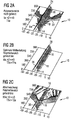
- Figures 2A, 2B and 2C show the attenuator 10 in three Operating modes Ia, IIa and IIIa.
- a wave is coupled into the waveguide core 14. This wave propagates towards the polymer area 18 out.
- 2A, 2B and 2C are respectively Intensity distributions are shown in a plane that is parallel to the substrate and in the middle of the waveguide cores 14.16 lies. The intensity results from the sum of the squares of amounts of the components of the electric field strength.
- FIG. 2A shows the operating mode Ia, in which the polymer range is not heated and has a temperature T1a.
- the refractive index n2 of the polymer region 18 is larger than the refractive index n3 and therefore also greater than the refractive index n1.
- the refractive index n2 of the polymer region 18 is thus larger than that of the material surrounding the polymer region 18 with the refractive index n1.
- the polymer region 18 can therefore be a Transmit wave that is coupled as an input shaft 20
- the refractive index n2 of the polymer region 18 differs from that Refractive index n3 of the waveguide core 14 or the waveguide core 16 deviates, form the boundaries between the polymer area 18 and the waveguide core 14 or the waveguide core 16 defects that lead to transmission losses.
- a Stray wave 22 low intensity compared to that of Waveguide core 14 is therefore coming input shaft 20 radiated into the waveguide layer 12.
- input wave is transmitted through the polymer region 18 and as an output shaft 24 using the waveguide core 16 forwarded.
- the operating mode Ia is in practice as an intermediate stage between the operating modes explained with reference to FIGS. 2B and 2C IIa and IIIa used.
- FIG. 2B shows the attenuator 10 in the operating mode IIa.
- the Temperature T2a of the polymer region 18 is in the operating mode IIa greater than the temperature T1a. Therefore is in the operating mode IIa the refractive index n2 of the polymer region 18 is the same the refractive index n3 of the waveguide core 14 or the waveguide core 16. This means that the polymer region 18 on the Waveguide core 14 and the waveguide core 16 adapted is.
- An input shaft 26 is in the waveguide core 14 coupled in and almost lossless via the polymer region 18 transmitted to the waveguide core 16 and appears at the output of the attenuator 10 as the output shaft 28.
- thermo-optical attenuator works in operating mode IIa thus as an almost lossless transmitting waveguide.
- FIG. 2C shows the thermo-optical attenuator 10 in one Operating mode IIIa, in which the polymer region 18 is even stronger is heated up than in operating mode IIa.
- the temperature T3a of the polymer region 18 is greater than the temperature T2a.
- the refractive index n2 of the polymer region 18 is lower than the refractive index n1 and therefore also smaller than the refractive index n3. Since the refractive index n2 of the polymer region 18 is less than is the refractive index n1 of the surrounding medium, the polymer range 18 in mode IIIa not as a waveguide work.
- the attenuator 10 influences the incoming wave the strongest. Is for example at the output of the attenuator 10, a sensor element arrives in operating mode IIIa the lowest energy on the sensor element.
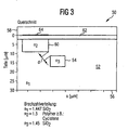
- FIG 3 shows the cross section of a thermo-optical attenuator 50 of a waveguide core in a waveguide layer 52 54 contains, which extends along the direction of propagation the waves are curved, see FIGS. 4A and 4B.
- the waveguide layer 52 consists of silicon dioxide with a refractive index n1 is 1.447.
- the waveguide core 54 also exists made of silicon dioxide, but has a refractive index equal to n3 1.45.
- the waveguide core 54 has a rectangular cross section and is dimensioned so that a light wave with a Wavelength of 1550 nanometers (nm) transmitted with almost no loss becomes.
- the attenuator 50 shows an abscissa axis 56 length values in a horizontal direction x-direction.
- An ordinate axis 58 shows length values in the y direction, which is perpendicular to the x direction.
- On the abscissa axis 56 and the ordinate axis 58 are length values in ⁇ m ablated.
- the waveguide core 52 has one in the x direction Expansion of approximately 6 ⁇ m and an expansion in the y direction of about 6 ⁇ m.
- Both in the x direction and in the y direction to the waveguide core 54 is offset a polymer region 60 with a rectangular shape Cross section arranged.
- the polymer region 60 runs parallel to a portion of the waveguide core 54 in the direction of propagation the waves, see Figures 4A and 4B.
- the Polymer region 60 is located further from one in the y direction not shown substrate removed as the waveguide core 54.
- a distance d between the top left edge of the waveguide core 54 and the lower right edge of the Polymer area 60 is only a few microns, for example 2 microns. Since the wave in both the waveguide core 54 and in the this waveguide core 54 immediately adjacent areas transmitted, it can pass through the polymer region 60 in its Spread can be influenced.
- the polymer region 60 consists of cyclotene and has at room temperature, i.e. at 20 ° C, a refractive index n2 approximately 1.5.
- the polymer region 60 adjoins one on the surface of the Polymer layer 62 lying on waveguide layer 52.
- On the Polymer layer 62 is located in the area of the polymer area 60 an electrode 64, which is designed as a heating element is.
- the attenuator 50 operates in one of two operating modes Ib and IIb, which are described below using the Figures 4A and 4B are explained.
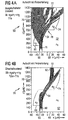
- Figures 4A and 4B show the thermo-optical attenuator 50 in two operating modes Ib and IIb.
- Figures 4A and 4B becomes a plane parallel to the substrate surface shown in plan view by the attenuator 50.
- the intensity distribution within the attenuator 50 is shown, that from one at an input 66 of the attenuator 50 coupled input shaft in the different operating modes Ib and IIb results.
- Figures 4A and 4B is also an abscissa axis 68 and an ordinate axis, respectively 70 shown on which length information in the unit ⁇ m are removed.
- the polymer region 60 has, for example a length of about 500 ⁇ m in the z direction.
- the waveguide core 54 is in its course from the entrance 66 to an output 72 of the attenuator 50 curved twice.
- the first curvature runs to the right and lies in the area of the Polymer region 60. Adjoining this is the waveguide core 54 curved to the left. It lies in the area of this curvature another polymer region 74, which is also made of a polymer with the refractive index n2.
- the polymer areas 60 and 74 each lie on the convex side in the course of the curvature of the waveguide core 54.
- FIG. 4A shows the attenuator 50 in the operating state Ib.
- T1b denotes the Temperature in polymer areas 60 and 74.
- T1b denotes the Temperature in polymer areas 60 and 74.
- In operating mode Ib is the refractive index n2 of the polymer regions 60 and 74 greater than the refractive index n1 or the refractive index n3.
- An input shaft 76 coupled at the input 66 is pulled and spread almost entirely into the polymer region 60 yourself out there. Step on the edges of the polymer region 60 Scattered waves 78, which are in the waveguide layer 52 spread out diffuse. At output 72 there is only one wave less Intensity on.
- the polymer region 74 weakens one in the waveguide core 54 transmitted residual wave.
- Operating mode Ib is used, for example, when a sensor element arranged at the output 72 in the idle state should.
- FIG. 4B shows the attenuator 50 in the operating mode IIb.
- the electrode 64 see FIG. 3, and the electrode disposed over the polymer region 74 Voltage and heat the polymer regions 60 and 74 to one Temperature T2b, which is above the temperature T1b of the operating state Ib lies. This reduces the value of the Refractive index n2 compared to the operating state Ib.
- the refractive index In operating state IIb, n2 is less than or equal to the refractive index n1 of the waveguide layer 52 and thus also smaller than that Refractive index n3.
- Coupled input shaft 80 is along the waveguide core 54 is transmitted to output 72 essentially undisturbed and appears there as output shaft 82.
- the attenuator 50 thus leaves i.e. in operating mode IIb, the input shaft 80 through. in the Operating state Ib, i.e. when the Attenuator 50, however, an input shaft 76 in the Waveguide layer 52 emitted. So the Use attenuator 50 also as a switch.
- FIG. 5 shows the top view of a thermo-optical switch 100, which has two waveguide cores in a waveguide layer 102 104 and 106 includes area 108 run parallel to each other.
- the waveguide layer 102 consists of silicon dioxide with a refractive index n1 equal 1.442.
- Waveguide cores 104 and 106 also exist made of silicon dioxide, but have a refractive index equal to n3 1,448.
- Waveguide core 104 extends from an input 110 to a working exit 112.
- the waveguide core 106 runs from section 108 to a resting exit 114.
- the polymer region 116 extends on the one hand parallel to the waveguide cores 104 and 106.
- polymer region 116 extends from the surface of the waveguide layer 102 to a depth into which the waveguide cores 104 and 106 are also sufficient.
- the waveguide cores 104 and 106 are in contrast to the polymer range 116 completely of the silicon dioxide of the waveguide layer surrounded by the refractive index n1.
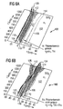
- FIGS. 6A and 6B show two operating modes Ic and IIc of the thermo-optical switch 100.
- The is shown Intensity distribution of the electrical component of an electromagnetic Wave in a through the central axes of the Waveguide cores 104 and 106 laid level. In the longitudinal direction of the Waveguide cores 104 and 106 are on the left side of the Level lengths are given in micrometers.
- the one shown Cutout is at z positions from 0 microns to about 1350 microns. Length information is at the bottom of the level the x direction in micrometers.
- the central axis of the waveguide core 104 is 0 micrometers.
- the in the Figures 6A and 6B planes extend from about -40 Micrometers to about 60 micrometers in the x direction.
- FIG. 6A shows the operating state Ic in which the polymer area 116 through the electrodes, not shown a temperature T1c is heated.
- T1c the refractive index n2 of the polymer region 116 is less than or equal to the refractive index n1 of the polymer region 116 and the waveguide cores 104 and 106 surrounding polymer layer 102.
- the Polymer region 116 can be due to the small refractive index n2 don't work as a waveguide.
- One at input 110 of the switch 100 coupled input shaft 118 is by the Waveguide core 104 practically unchanged from the work exit 112 is routed and appears there as output shaft 120 Operating mode Ic no wave occurs at the idle output 114.
- FIG. 6B shows the thermo-optical switch 100 in the operating mode IIc, in which the polymer region 116 is not heated will, d. H. the switch 100 is in the idle state.
- the changeover switch 100 operates a temperature T2c that is less than the temperature T1c.
- Due to the negative thermo-optical coefficient of the polymer area 116 is the value of the refractive index n2 at temperature T2c larger than at temperature T1c.
- the refractive index n2 of the polymer region 116 is larger in the operating mode IIc than the refractive index n3 of the waveguide cores 104 and 106 and thus also greater than the refractive index n1 of the waveguide layer 102.
- the Polymer region 116 spreads out in the waveguide core 112 Affect wave.
- the polymer region 116 works as Coupling area between the waveguide cores 104 and 106.
- An input shaft 122 at input 110 is in the area of the polymer area 116 coupled in the waveguide core 114 and appears at idle output 114 as output shaft 124.
- In operating mode IIc only appears from input shaft 122 a small part as a residual shaft 126 at the working output 112. Die The intensity of the residual wave 126 is orders of magnitude lower than the intensity of the output wave 124.
- FIGS. 7A, 7B and 7C show cross sections through a thermo-optical attenuator 150 according to an embodiment of the invention.
- Attenuator 150 contains a waveguide layer on a silicon substrate, not shown 152 made of silicon dioxide with a refractive index n1 equal to 1.442 at room temperature, i.e. H. at 20 ° C.
- n1 refractive index
- n3 Refractive index
- the polymer region 156 has transverse to the direction of propagation of waves the same cross section as that Waveguide core 154. At room temperature, i.e. at 20 ° C the polymer region 156 has a refractive index n2 equal to 1.5.
- the polymer area However, 156 runs only in a relatively short Section adjacent to the waveguide core 154, e.g. B. for a 500 micron range.
- Above the polymer area 156 and above the waveguide layer 152 is a thin teflon layer 158 with a layer height of about 2 micrometers applied. Teflon layer 158 has a refractive index which corresponds approximately to the refractive index n1. This prevents the Teflon layer 158 that waves from the polymer region 156 reach a heating electrode 160 that is above the polymer area 156 lies on the Teflon layer 158.
- the waveguide core 154 and the Polymer regions 156 each have an extension in the x direction of about 6 microns and also one in the y direction Expansion of about 6 microns.
- the polymer area is in the x direction 156 by an offset Vx of about 9 microns offset (from center to center). In the y direction there is also an offset Vy of about 9 microns. So that is the smallest distance between waveguide core 154 and polymer area 156 just a few micrometers. This leads to the propagation of a wave in the waveguide core 154 and in the area immediately around the waveguide core 154 the waveguide layer 152 using the polymer region 156 influences.
- the attenuator 150 with the help the heating electrode 160 by supplying a maximum heating power Pmax heated to a temperature T1d.
- the temperature is equal to the refractive index n2 of the polymer area the refractive index n1 is equal to 1.442, d. H. equal to the refractive index of the Waveguide layer 52 that surrounds polymer region 156.
- polymer region 156 cannot operate in Id mode work as a waveguide.
- One in the waveguide core 154 Coupled wave spreads and becomes unhindered not affected by polymer area 156.
- Figure 7A are Equi-intensity lines of such a wave plotted, e.g. B. the equi-intensity line 162.
- FIG. 7B shows the thermo-optical attenuator 150 in one Operating mode IId.
- the heating electrode 160 a heating power PH is supplied, which is less than is the maximum heating power Pmax of the heating electrode 160.
- the temperature T2d of the polymer region 156 in the Operating mode IId less than the temperature T1d. Due to the changed temperature is in operating mode IId Refractive index n2 of the polymer region 156 above the refractive index n1 the waveguide layer surrounding the polymer region 156 152.
- the refractive index n2 is equal to that Refractive index n3 of the waveguide core 154.
- Equi-intensity lines 164 and 166 include both the waveguide core 154 as well as the polymer region 156. Through this "Suction" will be the intensity of one in the waveguide core 154 propagating wave weakened.
- FIG. 7C shows the thermo-optical attenuator 150 in one Operating mode IIId, in which the heating electrode 160 in the voltage-free Condition is.
- the heating power PH is 0 watts.
- the Temperature T3d of the polymer region 156 is below that Temperature T2d.
- the refractive index n2 of the polymer region lies 156 over the refractive index n3 of the waveguide core 154 and also over the refractive index n1 of the waveguide layer 152, which also surrounds the polymer region 156.
- the polymer area 156 is therefore better in mode IIId for guiding one Wave suitable as the waveguide core 154.
- the one in Figure 7C is at the end of the polymer region 156 by a wave entering the attenuator 150 reached later than the other end of polymer region 156 becomes.
- a wave that propagates in the core of the waveguide becomes complete up to the cross section shown in Figure 7C from the waveguide core 154 into the polymer area 156 coupled.
- Equi-intensity lines 168 therefore include polymer area 156 only.
- Attenuator 150 shown in FIGS. 7A, 7B and 7C can thus be used as a switch, for example.
- the Operating mode Id gets a wave through the Attenuator 150.
- mode IIId is the "Switch" interrupted and an incoming wave can Waveguide region 154 does not pass because it is in the polymer region 156 is coupled over.
- Attenuator 150 is used for signal adaptation, then all three operating modes Id, IId and IIId are used.
- On Sensor element is located, for example, at the exit of the Waveguide core 154.
- the operating mode Id one in the Wave entering the shaft freely to the sensor element transfer.
- mode IId only a part of it arrives of the wave coupled into the waveguide core 154 to the sensor element.
- mode IIId one can be in the waveguide core 154 propagating wave, however, not to the sensor element reach.
- FIGS 8A, 8B and 8C show cross sections through a thermo-optical absorber 170 according to an embodiment of the invention.
- a waveguide layer 172 made of silicon dioxide with a refractive index n1 equal to 1.422 20 ° C.
- n1 refractive index
- n3 refractive index
- the waveguide core 174 has a square one Cross section, however, due to the distorted representation appears rectangular in Figures 8A, 8B and 8C.
- a polymer region 176 is introduced in the waveguide layer 172. It was initially parallel to the course of the waveguide core 176 a trench with a length of about 300 micrometers etched. Then a polymer, e.g. B. Cycloten, with Introduced into the trench using a spinning process. This created on the surface of the waveguide layer 172 a polymer layer 178.
- the polymer region 176 and the polymer layer 178 have a refractive index n2 equal to 1.5 at room temperature of 20 ° C.
- FIGs 8A, 8B and 8C are at the bottom and on the left Border dimensions for the horizontal x-direction and the vertical y direction in micrometers.
- the waveguide core 174 and polymer area 176 are square Cross section of 6 microns by 6 microns.
- the polymer area 176 is in the x direction with respect to the waveguide core 174 and offset by 9 micrometers in the y direction (Center to center).
- the polymer region 176 is thus located so close to the waveguide core 174 that one using the waveguide core 174 transmitted wave depending on the refractive index n2 of the polymer region 176 can be influenced.
- FIG. 8A shows an operating mode Ie of the thermo-optical absorber 170, in which a heating electrode 180 with maximum heating power Pmax is operated.
- the heating electrode 180 is located immediately above polymer area 176 on the polymer layer 178.
- the polymer area heats up 176 to a temperature T1e.
- the polymer region 176 has a refractive index n2 that is the same the refractive index is n1.
- n2 refractive index
- This allows the polymer region 176 in the Operating mode Ie does not work as a waveguide.
- the operating mode Ie is coupled into the waveguide core 174 Wave unaffected by polymer area 176 passed this.
- Equi-intensity lines 182 include therefore only the waveguide core 174.
- Figure 8B shows an operating mode IIe in which the electrode 180 is operated with a heating power PH that is less than the maximum heating power is Pmax.
- a temperature T2e of the Polymer area 176 in mode IIe is therefore smaller than the temperature T1e. Because of the lower temperature T2e has a refractive index n2 in the polymer region 176 one that is equal to the refractive index n3 and therefore also greater than the refractive index is n1.
- the polymer region 176 can be a due to these refractive indices Guide and draw part of a wave using the waveguide core 174 transported wave, compare equi-intensity line 184 and 186, both the polymer range 176 as well as the waveguide core 174.
- the one in the polymer area 176 guided wave is however through the heating electrode 180 absorbed. Absorbing the shaft with the help the heating electrode 180 causes that in the waveguide layer 172 less energy is emitted than with the of Figures 7A, 7B and 7C explained optothermal Attenuator 150.
- FIG 8C shows an operating mode IIIe, in which the heating electrode 180 is de-energized and therefore switched off.
- the heating power PH is therefore 0 watts.
- T3e denotes the temperature in the polymer region 176.
- the temperature T3e is less than the temperature T2e in the operating mode IIe. Due to the lower temperature T3e is in mode IIIe, the refractive index n2 of the polymer region 176 larger than the refractive index n3 in the waveguide core 174 and also greater than the refractive index n1 of the waveguide layer 172 of these refractive indices, the polymer region 176 is suitable better for transporting a light wave from, for example 1550 nanometers as the waveguide core 174.
- a wave is coupled into the waveguide core 174, this wave is like that shown in Figure 8C Cross section at the end of the polymer region 176 almost completely transitioned into the polymer region 176, see equi-intensity lines 188, which only comprise the polymer region 176.
- the wave conducted in the polymer region 176 is caused by the Heating electrode 180 almost completely absorbed.
- the radiation into the waveguide layer 172 is small.
- FIGS. 4A, 4B; 7A, 7B, 7C; 8A, 8B and 8C explained components 60, 74, 156, 176 polymers are used in the polymer range, dampen the waves strongly. The one achieved with the components Weakening thereby further increases.
- polymers are used with others Properties used, e.g. with a positive thermo-optical Coefficients. This allows the switching behavior in the idle state and in the operating state of the respective component turning back.
Landscapes
- Physics & Mathematics (AREA)
- Nonlinear Science (AREA)
- General Physics & Mathematics (AREA)
- Optics & Photonics (AREA)
- Optical Integrated Circuits (AREA)
- Optical Modulation, Optical Deflection, Nonlinear Optics, Optical Demodulation, Optical Logic Elements (AREA)
Claims (7)
- Dispositif de guide d'ondes intégré, comportant:caractérisé en ce queune zone (152 ; 172) de guide d'ondes constituée de verre, dans laquelle est disposé un guide d'ondes avec un noyau en verre (154 ; 174) et une enveloppe en verre s'étendant le long d'une direction de propagation d'ondes,une zone étrangère (156 ; 176) en un matériau autre que du verre s'étendant à proximité du guide d'ondes, etune unité de régulation de température (160 ; 180) destinée au chauffage et/ou au refroidissement de la zone étrangère (156 ; 176), moyen par lequel la propagation des ondes dans le guide d'ondes peut être influencée,la zone étrangère (156 ; 176) étant intégrée dans la zone (152 ; 172) de guide d'ondes ;la zone (152 ; 172) de guide d'ondes étant disposée sur un substrat plan, et formant sur la face opposée au substrat une surface située pour l'essentiel parallèlement à l'interface entre le substrat et la zone (152 ; 172) de guide d'ondes ;la zone étrangère (156 ; 176) étant décalée par rapport au guide d'ondes transversalement à la direction de propagation des ondes, aussi bien parallèlement que perpendiculairement à l'interface entre le substrat et la zone (152 ; 172) de guide d'ondes ; etla zone étrangère (156 ; 176) s'étendant pour l'essentiel parallèlement au guide d'ondes ;
le noyau en verre (154 ; 174) du guide d'ondes et la zone étrangère (156 ; 176) ont sensiblement la même section transversale du point de vue dimensions et formes. - Dispositif de guide d'ondes selon la revendication 1,
caractérisé en ce que la zone étrangère (156 ; 176) est un matériau ayant un coefficient thermo-optique dont la valeur est nettement supérieure à la valeur du coefficient thermo-optique du verre et qui, du point de vue valeur, est nettement supérieur au coefficient thermo-optique du verre, notamment plus de quatre vingt fois supérieur. - Dispositif de guide d'ondes selon l'une quelconque des revendications précédentes,
caractérisé en ce que la zone étrangère (156 ; 176) contient un polymère de fluoroacrylate ou un polymère à base de benzocyclobutène. - Dispositif de guide d'ondes selon l'une quelconque des revendications précédentes,
caractérisé en ce que la zone étrangère (156 ; 176) s'étend de la surface de la zone (152 ; 172) de guide d'ondes opposée au substrat jusqu'à proximité du guide d'ondes comportant le noyau en verre (154 ; 174). - Dispositif de guide d'ondes selon l'une quelconque des revendications précédentes,
caractérisé en ce que l'indice de réfraction (n3) du noyau (154 ; 174) du guide d'ondes est supérieur à l'indice de réfraction (n1) de l'enveloppe en verre du guide d'ondes,
et en ce qu'en fonction de la température engendrée par l'unité de régulation de température (160 ; 180), l'indice de réfraction (n2) du matériau de la zone étrangère (156 ; 176) est inférieur, égal ou supérieur à l'indice de réfraction (n1) de l'enveloppe en verre du guide d'ondes. - Dispositif de guide d'ondes selon l'une quelconque des revendications précédentes,
caractérisé en ce qu'une couche intermédiaire (158) est disposée entre l'unité de régulation de température (160) et la zone étrangère (156), laquelle est en un matériau qui empêche qu'une onde se propageant dans la zone étrangère (166) arrive à l'unité de régulation de température (160). - Dispositif de guide d'ondes selon l'une quelconque des revendications précédentes,
caractérisé en ce qu'une couche intermédiaire (178) est disposée entre l'unité de régulation de température (180) et la zone étrangère (176), laquelle est en un matériau ayant le même indice de réfraction que la zone étrangère (176), et en ce que l'unité de régulation de température (180) est disposée sur la couche intermédiaire (178) directement au-dessus de la zone étrangère (176), de sorte qu'une onde se propageant dans la zone étrangère puisse être absorbée dans l'unité de régulation de température (180).
Applications Claiming Priority (2)
| Application Number | Priority Date | Filing Date | Title |
|---|---|---|---|
| DE10032933 | 2000-07-06 | ||
| DE10032933A DE10032933B4 (de) | 2000-07-06 | 2000-07-06 | Integrierte Wellenleiteranordnung |
Publications (2)
| Publication Number | Publication Date |
|---|---|
| EP1170621A1 EP1170621A1 (fr) | 2002-01-09 |
| EP1170621B1 true EP1170621B1 (fr) | 2004-03-17 |
Family
ID=7648050
Family Applications (1)
| Application Number | Title | Priority Date | Filing Date |
|---|---|---|---|
| EP01116402A Expired - Lifetime EP1170621B1 (fr) | 2000-07-06 | 2001-07-06 | Dispositif de guide d'onde optique intégré |
Country Status (3)
| Country | Link |
|---|---|
| US (1) | US6671439B2 (fr) |
| EP (1) | EP1170621B1 (fr) |
| DE (1) | DE10032933B4 (fr) |
Families Citing this family (4)
| Publication number | Priority date | Publication date | Assignee | Title |
|---|---|---|---|---|
| EP1327903A1 (fr) * | 2002-01-14 | 2003-07-16 | Alcatel | Déphaseur optique de guide d'ondes |
| US6975793B2 (en) * | 2002-03-18 | 2005-12-13 | Lightwave Microsystems Corporation | Method and apparatus facilitating mechanical beam steering for optical integrated circuits |
| DE10246547B4 (de) | 2002-09-30 | 2008-05-15 | Finisar Corp., Sunnyvale | Brechungsindexgitter und Modenkoppler mit einem Brechungsindexgitter |
| US7079747B1 (en) | 2004-03-01 | 2006-07-18 | Photintech Inc. | Three dimensional thermo-electro-mechanical device for controlling light propagation in an optical guide |
Family Cites Families (15)
| Publication number | Priority date | Publication date | Assignee | Title |
|---|---|---|---|---|
| FR2683054B1 (fr) * | 1991-10-25 | 1993-12-03 | Commissariat A Energie Atomique | Modulateur electrooptique integre et procede de fabrication de ce modulateur. |
| US5739948A (en) * | 1995-10-12 | 1998-04-14 | Dow Corning Asia, Ltd. | Refractive index modulation device and method of refractive index modulation |
| JPH1090636A (ja) * | 1996-09-13 | 1998-04-10 | Nippon Telegr & Teleph Corp <Ntt> | 光半導体装置 |
| JP3713942B2 (ja) | 1998-02-20 | 2005-11-09 | 日立電線株式会社 | 導波路型光スイッチ |
| US6002823A (en) | 1998-08-05 | 1999-12-14 | Lucent Techolonogies Inc. | Tunable directional optical waveguide couplers |
| US6240226B1 (en) | 1998-08-13 | 2001-05-29 | Lucent Technologies Inc. | Polymer material and method for optical switching and modulation |
| EP0987580A1 (fr) * | 1998-09-16 | 2000-03-22 | Akzo Nobel N.V. | Modulateur d'intensité lumineuse et commutateur le comprenant |
| US6385383B1 (en) | 1998-10-05 | 2002-05-07 | Lucent Technologies Inc. | Optical attenuator structure and method using polymer material |
| US6144780A (en) | 1998-10-05 | 2000-11-07 | Lucent Technologies Inc. | Polymer waveguide switch and method |
| DE19849862C1 (de) * | 1998-10-29 | 2000-04-06 | Alcatel Sa | Thermooptischer Schalter |
| CA2346130A1 (fr) * | 1998-11-10 | 2000-05-18 | Lightwave Microsystems Corporation | Dispositifs photoniques comprenant un polymere thermo-optique |
| EP1018665B1 (fr) | 1999-01-05 | 2004-03-17 | Corning Incorporated | Commutateur thermo-optique asymétrique |
| US6236774B1 (en) * | 1999-03-22 | 2001-05-22 | Gemfire Corporation | Optoelectronic and photonic devices formed of materials which inhibit degradation and failure |
| EP1234199A1 (fr) * | 1999-12-02 | 2002-08-28 | Gemfire Corporation | Photodefinition de dispositifs optiques |
| GB2358712A (en) | 2000-01-28 | 2001-08-01 | Kymata Ltd | Optical Device |
-
2000
- 2000-07-06 DE DE10032933A patent/DE10032933B4/de not_active Expired - Fee Related
-
2001
- 2001-07-05 US US09/899,493 patent/US6671439B2/en not_active Expired - Lifetime
- 2001-07-06 EP EP01116402A patent/EP1170621B1/fr not_active Expired - Lifetime
Also Published As
| Publication number | Publication date |
|---|---|
| EP1170621A1 (fr) | 2002-01-09 |
| DE10032933B4 (de) | 2004-07-15 |
| DE10032933A1 (de) | 2002-01-17 |
| US6671439B2 (en) | 2003-12-30 |
| US20020025120A1 (en) | 2002-02-28 |
Similar Documents
| Publication | Publication Date | Title |
|---|---|---|
| DE3889364T2 (de) | Optischer Wellenleiter und Verfahren zu seiner Herstellung. | |
| DE69220951T2 (de) | Nahfeld-Phatonentunnelvorrichtungen | |
| DE69523094T2 (de) | Faseroptischer Isolator | |
| DE60118264T2 (de) | Polarisationsunabhängige optische Wellenleiterschaltung | |
| DE3486165T2 (de) | Integrierte optische schaltung. | |
| EP1008013B1 (fr) | Commutateur thermo-optique | |
| DE69128866T2 (de) | Optische Schaltung mit Y-Verzweigung | |
| DE69223885T2 (de) | Optischer Schalter | |
| DE19849862C1 (de) | Thermooptischer Schalter | |
| DE3687920T2 (de) | Elektrooptischer welleneleitermodulator. | |
| DE4212208A1 (de) | Verfahren zur Herstellung optischer Polymerbauelemente mit integrierter Faser-Chip-Kopplung in Abformtechnik | |
| DE69018041T2 (de) | Optischer Schalter zur Verwendung mit optischen Fasern. | |
| DE68913782T2 (de) | Polarisationsunabhängiger optischer Wellenleiterschalter. | |
| DE19711507A1 (de) | Optische Verzweigungs-/Kreuzungs-Wellenleiterschaltung | |
| DE69102450T2 (de) | Integriert optischer Polarisationsteiler. | |
| EP0037006A1 (fr) | Coupleur-étoile optique avec dispositif mélangeur planaire | |
| DE60127146T2 (de) | Optische vorrichtung | |
| EP1170621B1 (fr) | Dispositif de guide d'onde optique intégré | |
| EP3545347B1 (fr) | Composant optoélectronique et procédé de fabrication d'un composant optoélectronique | |
| EP0740802B1 (fr) | Procede de fabrication d'une composante optique integre | |
| EP0822424B1 (fr) | Dispositif de branchement optique | |
| DE10246547B4 (de) | Brechungsindexgitter und Modenkoppler mit einem Brechungsindexgitter | |
| DE102024200644B3 (de) | Mehrlagige Signalleitstruktur und Verfahren zum Betreiben einer mehrlagigen Signalleitstruktur | |
| DE19929250A1 (de) | Lichtintensitätsmodulator und Verfahren zu seiner Herstellung | |
| DE69737491T2 (de) | Integrierte optische Einrichtung mit aktiven und passiven Wellenleiterbereichen |
Legal Events
| Date | Code | Title | Description |
|---|---|---|---|
| PUAI | Public reference made under article 153(3) epc to a published international application that has entered the european phase |
Free format text: ORIGINAL CODE: 0009012 |
|
| AK | Designated contracting states |
Kind code of ref document: A1 Designated state(s): FR GB Kind code of ref document: A1 Designated state(s): AT BE CH CY DE DK ES FI FR GB GR IE IT LI LU MC NL PT SE TR |
|
| AX | Request for extension of the european patent |
Free format text: AL;LT;LV;MK;RO;SI |
|
| 17P | Request for examination filed |
Effective date: 20020704 |
|
| AKX | Designation fees paid |
Free format text: FR GB |
|
| REG | Reference to a national code |
Ref country code: DE Ref legal event code: 8566 |
|
| 17Q | First examination report despatched |
Effective date: 20020918 |
|
| RTI1 | Title (correction) |
Free format text: INTEGRATED OPTICAL WAVEGUIDE DEVICE |
|
| GRAP | Despatch of communication of intention to grant a patent |
Free format text: ORIGINAL CODE: EPIDOSNIGR1 |
|
| RTI1 | Title (correction) |
Free format text: INTEGRATED OPTICAL WAVEGUIDE DEVICE |
|
| GRAS | Grant fee paid |
Free format text: ORIGINAL CODE: EPIDOSNIGR3 |
|
| GRAA | (expected) grant |
Free format text: ORIGINAL CODE: 0009210 |
|
| AK | Designated contracting states |
Kind code of ref document: B1 Designated state(s): FR GB |
|
| REG | Reference to a national code |
Ref country code: GB Ref legal event code: FG4D Free format text: NOT ENGLISH |
|
| REG | Reference to a national code |
Ref country code: IE Ref legal event code: FG4D Free format text: GERMAN |
|
| GBT | Gb: translation of ep patent filed (gb section 77(6)(a)/1977) |
Effective date: 20040510 |
|
| REG | Reference to a national code |
Ref country code: IE Ref legal event code: FD4D |
|
| ET | Fr: translation filed | ||
| PLBE | No opposition filed within time limit |
Free format text: ORIGINAL CODE: 0009261 |
|
| STAA | Information on the status of an ep patent application or granted ep patent |
Free format text: STATUS: NO OPPOSITION FILED WITHIN TIME LIMIT |
|
| 26N | No opposition filed |
Effective date: 20041220 |
|
| PGFP | Annual fee paid to national office [announced via postgrant information from national office to epo] |
Ref country code: GB Payment date: 20070727 Year of fee payment: 7 |
|
| PGFP | Annual fee paid to national office [announced via postgrant information from national office to epo] |
Ref country code: FR Payment date: 20070717 Year of fee payment: 7 |
|
| GBPC | Gb: european patent ceased through non-payment of renewal fee |
Effective date: 20080706 |
|
| REG | Reference to a national code |
Ref country code: FR Ref legal event code: ST Effective date: 20090331 |
|
| PG25 | Lapsed in a contracting state [announced via postgrant information from national office to epo] |
Ref country code: GB Free format text: LAPSE BECAUSE OF NON-PAYMENT OF DUE FEES Effective date: 20080706 |
|
| PG25 | Lapsed in a contracting state [announced via postgrant information from national office to epo] |
Ref country code: FR Free format text: LAPSE BECAUSE OF NON-PAYMENT OF DUE FEES Effective date: 20080731 |